AMAZON multi-meters discounts AMAZON oscilloscope discounts
Printed-circuit (PC)-board development and improvement have been slow but continuous since the switch from the wired connection of all components to the printing of circuits, which began in the 1950s. This development is still continuing, possibly at a more rapid pace with the introduction of surface-mounted parts.
However, the drawing or layout of printed circuits has not changed much in recent years. More of this drawing is being done by computer-aided equipment, of course. But every day, somewhere, hundreds of persons are making drawings on drafting tables of printed circuits for new products.
In general, two systems are employed to place a printed or plated circuit on a circuit board. One method is to use a copper-clad laminate (board) and etch away the unwanted copper foil, leaving the desired circuit pattern. In this system a plating resist is applied in the image of the desired pattern. The board is subjected to the etching process, wherein that portion of the copper that is not covered by the resist is removed. One of several methods is employed to get the resist pattern onto the board.
The other process is the additive one, in which the conductor pattern is deposited on the board. Usually this is copper. Tin lead is then deposited on the copper by the electroplating process. After large mounting holes, if any, are made and gold connection tips, if any, are added, the circuit board undergoes a reflow process. During this process the copper and tin paths become solder, and the component connections are soldered to their respective conductor paths at their pads or plated-through holes.
Often a solder-resistant plastic is printed over the side of the board that has the solder and covers those areas that are to have no solder. This solder mask prevents solder from bridging closely spaced conductors and splashing on other unwanted places.
Regardless of how the PC board is to be manufactured, the layout of the final artwork is pretty much standard. Considerable thought and drafting go into the layout. A study of the calculator board ( FIG. 1) should indicate to the reader that careful layout of components and conductor paths is required.
The most recent version of what is essentially the same calculator (FIG. 2) shows a less complex board but the same orderly drawing and printing of conductor paths. This flexible laminated “board” is transparent: You are looking at the component side and seeing the circuit paths which are printed on the same side and covered with a protective coating. The board shown in FIG. 1 has printed wiring on both sides. The latest model of calculator costs a little more than half of what the earlier (by 7 to 8 years) model cost.
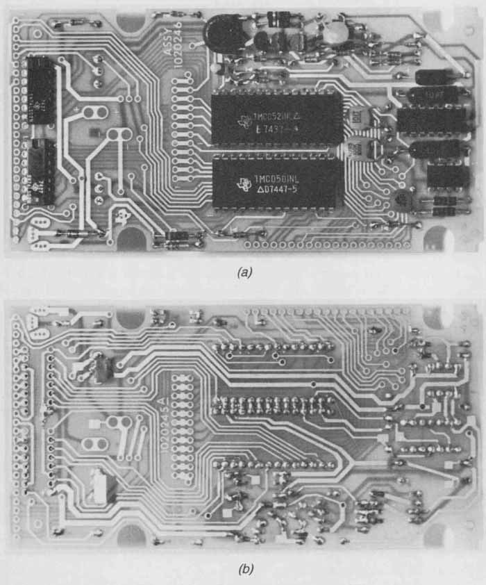
FIG. 1 Printed-circuit board for a scientific calculator: (a) component
side; (b) foil side. (Texas Instruments, Inc. and Precision Arts, Ltd.)
1 Making Drawings for a Printed Circuit
The first step in making a set of drawings for a printed circuit is to study the elementary diagram. Such a study will provide such information as:
1. What groups of components have common connections
2. What the peak potential differences will be
3. Grounds, voltage supply lines, etc., that are required
4. Ground paths, large and heavy, and heat sinks that will be necessary
5. Other pertinent information
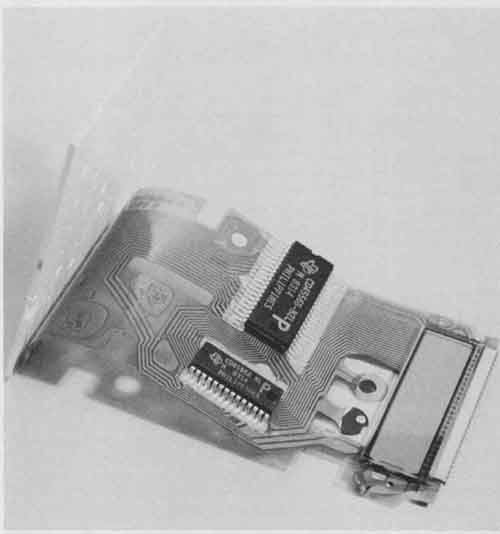
FIG. 2 Printed-circuit board for the most recent model of the scientific
calculator. The two ICs have replaced six ICs and about 18 discrete components
that were in the older model. (Texas Instruments, Inc.)
The next step is to make a preliminary sketch from the schematic diagram, such as that shown in Fig. 4-22a. The components involved in this circuit are mostly capacitors* (C1, C2, etc.), resistors (R1, R2, etc.), two transistors (PN2222) which we shall call Q1 and Q2 and an integrated amplifier circuit IC I. In the sketch (or sketches, because there may be several trials before the most likely pattern results), all components are located and circuit paths are sketched in. This is in reality a rough wiring diagram. Such a diagram was made before the component layout in Fig. 4-22c could be made. A preliminary sketch, in which the final component layout was used and freehand sketching of circuit paths was begun in the left portion, is shown in FIG. 3. (Since we are looking at the component side and because the printing of circuit paths is usually done on the other side, the final drawing should be made for the other or “foil” side.) Now this sketch can be checked to determine whether:
1. crossovers are zero or a minimum.
2. Bypass and grid lines are as short as possible.
3. Longer lines, such as ground and high-current, are placed near or around the edge of the board.
4. The design is neat and compact.
5. Other specifications (see Sec. 5-4) are met.
* In the figure, letters and subscripts appear in the same height (for example. C1).
Figures 4-22 and 3 show the final component layout as seen looking at the component side of the CB-receiver board. The components, as mentioned before, have been drawn so that their leads will pierce the board at the intersection of the 0.10-in. (2.54-mm) grid lines. FIG. 5 shows two grids that are frequently used. Not shown is a 0.05-in. (1.27-mm) grid system. The 0.05 (or 50-mil) grid is becoming quite popular because of its compatibility with surface-mounted devices to be explained later. The 50-mil grid is similar to the 100-mil (0.1-in.) grid, except that the holes are “centered” 0.05 in. apart. Through connections for grid systems are shown in FIG. 5c and d.
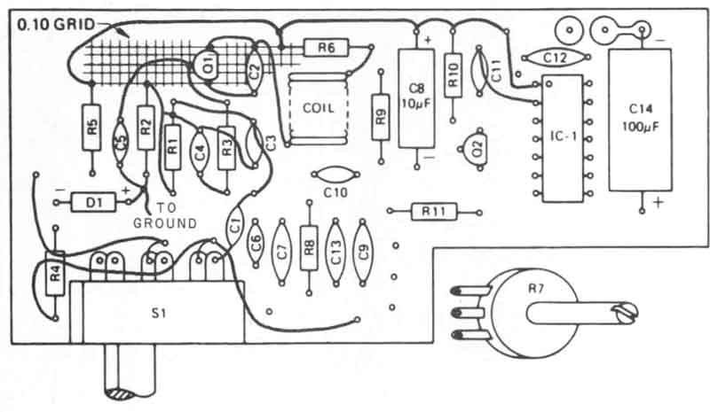
FIG. 3 A preliminary sketch for the layout (artwork) of a PC board.
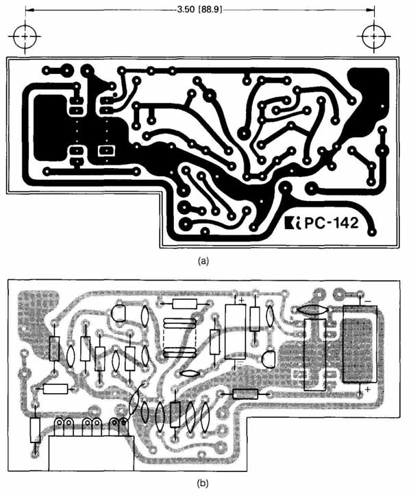
FIG. 4 (a) Final layout (final artwork) for a CB receiver, foil side.
(b) Component layout of CB PC board. (Kantronics, Inc. and Bishop Graphics,
Inc.)
In order to position components properly it is necessary to know their size, how far apart their leads must be placed, and how close together the components may be positioned on a board. Table 1 and FIG. 6 supply this information for many of the more frequently used components.
The final artwork for the CB circuit board is shown in FIG. 4a. It was done by a company that specializes in PCB layout with adhesive aids. The ground path is shown extending from the upper right corner, going down in the right center part, and then going up to the integrated circuit and capacitor, upper left. It is extra wide and heavy at each end and thus acts as a heat sink in those areas. (A heat sink removes heat by radiating it away from heat-producing elements.)
TABLE 1 Component Spacing on PC Boards
Note: Dimensions at left are in inches. Those in parens are in millimeters.
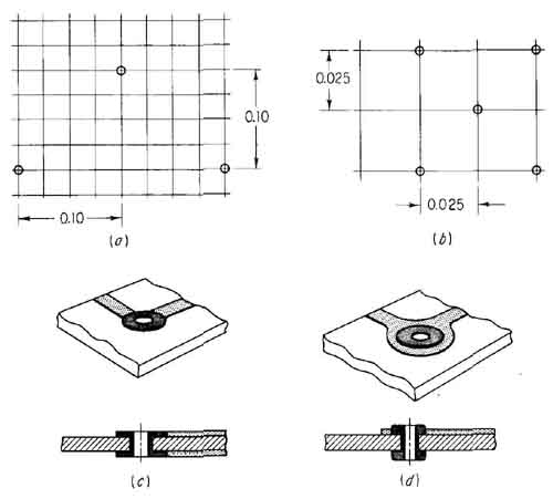
FIG. 5 Grid systems and through connections: (a) 0.10-in. (2.54-mm)
grid; (b) 0.025-in. (0.635-mm) grid; (C) plated hole connection; (d)
plated eyelet.
This PC board is a single-sided circuit board with components on one side and printed wiring on another. A photograph of the wiring side of the manufactured CB receiver PC board is shown in FIG. 9. As in the case of many similar products, the circuit paths were made by the etching process, in which a thin layer of conducting material (called a foil) is bonded to one side of the board and then etched away so that only the conductor paths remain.
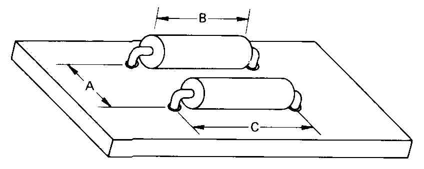
FIG. 6 Axial lead spacing for resistors and tubular-shaped components.
(See Table 1.) (King Radio Corp.)
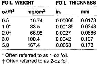
TABLE 2 Weight and Thickness of Copper Foils for PC Boards
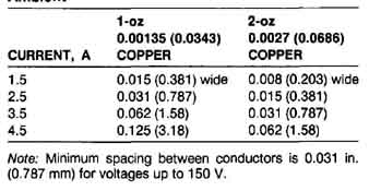
TABLE 3 Width of Conductor Paths in Relation to Current for a 40°C
Temperature Rise above Ambient
Note: Minimum spacing between conductors is 0.031 in. (0.787 mm) for voltages up to 150 V.
The final artwork or master layout of the CB-receiver circuit board of FIG. 4 was made by placing FIG. 4b upside down and then putting a standard acetate medium over it and applying commercially available tape and PC patterns. This single-sided PC board has served as a typical example. Later, a double-sided board layout will be presented.
The great bulk of PC boards are made from a paper-base phenolic or a glassy epoxy laminate, called G-10, which is superior to the phenolic in that it has a higher resistance to warping. They are of several standard thicknesses ranging from (0.79) to in. (6.35 mm). Copper foil comes in several thick nesses or weights as shown in Table 2. The cross section of the conductor should be large enough to carry the required current with a certain temperature rise. Table 3 is a partial table that provides some of this information for a 40°C rise above the ambient temperature (that which exists in the immediate environment).
2 Use of Tape and Other Contact-Adhesive Aids
Making a PC-board layout with tape is not quite as easy as it looks to the beginner. The preprinted appliqués (contact-adhesive patterns) are usually easy enough to separate from their protective backing. However, getting them on the exact desired location and oriented correctly is difficult for the person who has no experience or correct tools. (The latter should include a very sharp X-acto knife or equivalent and a thin, flat spatula-type tool for manipulating the pattern onto the drawing medium.) Getting a straight line with tape also re quires experience. One way is to hold the tape down at its starting point (usually on a pad which has already been emplaced), pull it slightly at the other end, and then lay it down and cut it to the desired length. One must try to allow for the stretching of the tape. Unfortunately, the tape is not supposed to be stretched, and the manufacturer’s instructions so indicate. The key to this approach is the word slightly, for as the authors and many others have discovered, it is extremely difficult to get a straight line if the tape is not stretched.
Pads and registration marks are usually put down first, then conductor paths, grounds, and heat sinks (if any) are added. Mylar for this artwork is available with grid lines spaced 0.050 (1.27), 0.100 (2.54), or 0.125 in. (3.18 mm) apart. Such a grid may be placed under a clear sheet of Mylar, which is to be the final artwork (master layout), or a grid with blue or brown “dropout” lines’ may itself be used for the master layout. When the tape is laid down, it should overlap onto the adjacent part of the lands, elbows, etc. (see FIG. 7).
It is very convenient to have 90-degree elbows available commercially, but not all corners are 90-degree. Other bends can be made with tape if one crimps it on the inside radius; or they can be done with ink, in which case one makes a line the same width as the tape. It is also possible to obtain 45-degree elbows commercially.
[These lines will not appear on the photographic reproduction.]
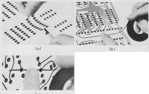
FIG. 7 (a) Putting a “stick-on” pattern on a PC-board layout; (b) and
(C) applying tape for long circuit path and short path distances. (Bishop
Graphics, Inc.)
The contact-adhesive aids shown in FIG. 8 deserve some comment. First, the dimensions listed are full, or actual, size. (The original drawing was reduced to about half size to fit in this guide). Second, the aids come in a number of different sizes (widths, in the case of lines). Conductor tapes are available 0.015 (0.38), 0.020 (0.51), 0.026 (0.66). 0.031 (0.787), 0.040 (1.02), 0.046 (1.17), 0.050(1.27), 0.062(1.57), 0.090(2.29), 0.100(2.54), and up to 2 in. (50.8 mm) wide. Some patterns are such that they can be cut to desired lengths ( FIG. 8d), and some are in fixed sizes ( FIG. 8e and f). FIG. 8i represents a set of lands which have the same center-to-center spacing as FIG. 8e. But the pads are small enough that a small conductor can be placed between them as shown — a situation that is sometimes unavoidable. Otherwise the larger pads are preferred because they provide better soldering and are more stable if a lead or component has to be removed and replaced. The IC connector pattern ( FIG. 8e) is available in different sizes and shapes. An optional arrangement is to buy flatpack patterns which have long “fingers” resembling FIG. 8d. The outline of the IC package can be drawn over the pattern, which can be trimmed to the exact size and shape with a small knife.
Target patterns ( FIG. 8g) are designed so that when superimposed any slight mismatching can be seen and corrected. Land or donut patterns ( FIG. 8h) are available in many sizes and combinations of inner and outer diameters. Careful attention must be given to inner diameters because different wire sizes are often present in any single printed circuit. Thus, wires to speakers, potentiometers, and outside power, for example, are usually larger than the leads to typical components on the board ( FIG. 9).
Our master layout was drawn to a 2: 1 scale (twice size). Scales of 2: 1 and 4: 1 are common, but 10: 1 and even 100: 1 have been used where extreme accuracy has been required. Tapes and aids can be obtained for most of these scales. For instance, a 0.062-in. (1.57-mm) tape on a 2:1-scale layout will produce a line that is actually 0.031 in. (0.787 mm), which is large enough to accommodate most currents ( Table 3).
The checklist that follows later provides other specifications for good PC- board layout. FIG. 4a includes two reduction targets with the required final dimension provided so that the finished product will be the desired size. More accurate layouts can be made with the coordinatograph ( FIG. 10, which has a plotting accuracy of 0.001 in. (0.0254 mm).
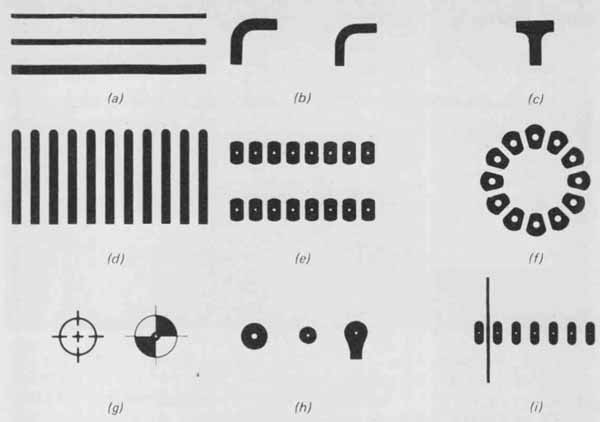
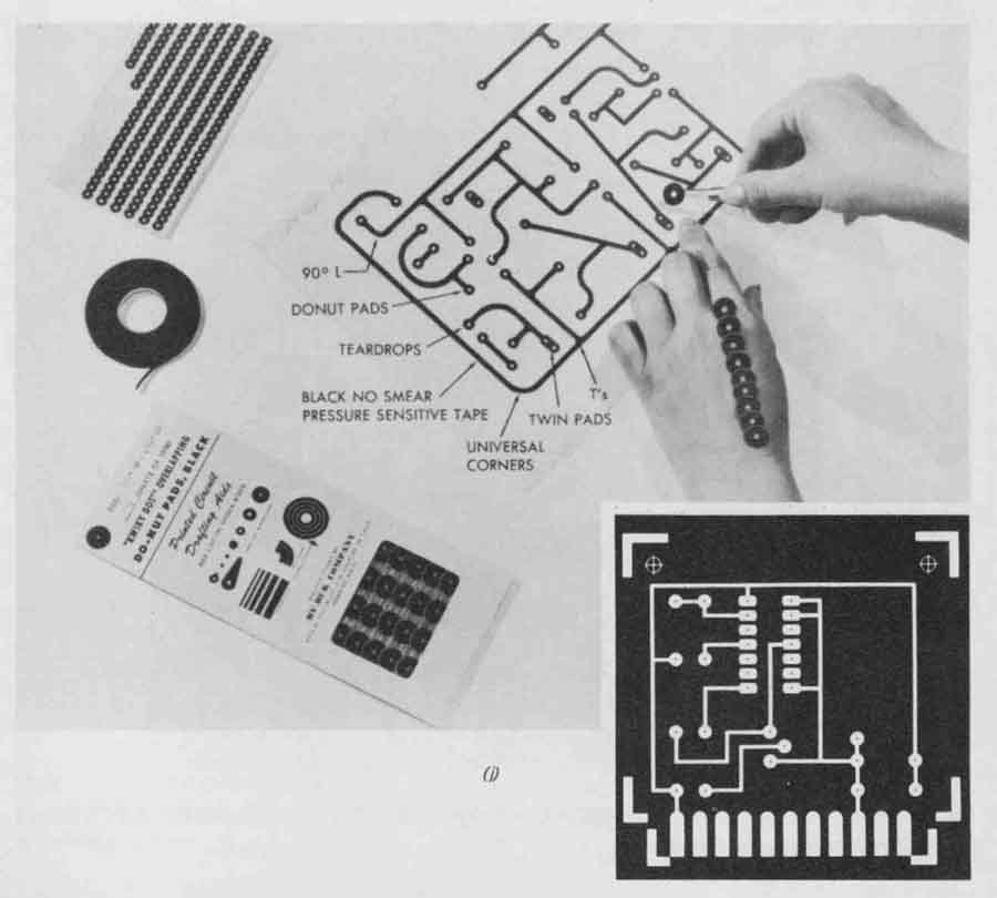
FIG. 8 Commercially available contact adhesive aids for PC-board drawings:
(a) conductor tapes, 0.046 in. (1.17 mm), 0.050 in. (1.27 mm), and 0.10
in (2.54 mm) wide; (b) 90 elbows or bends 0.125 in. (3.18 mm) and 0.10
in. (2.54 mm) wide or thick; (c) Tee 0.125 in. (3.18 mm); (d) connector
pattern, 0.20 in. (5.08 mm) center to center; (e) 16-lead DIP pattern
0.20 in. (5.08 mm) center to center;(f) 12-lead TO-5 pattern 0.74 in.
(19 mm) outer diameter, 0.075 in. (1.91 mm) inner diameter; (g) target
or registration marks; (h) pads or lands 0.281 in. (7.14 mm) outer diameter,
0.062 in. (1.58 mm); (1) seven-lead pad pattern, 0.20 in. (5.08 mm) center
to center, with conductor-path tape between two lands; (j) older appliqué
examples.
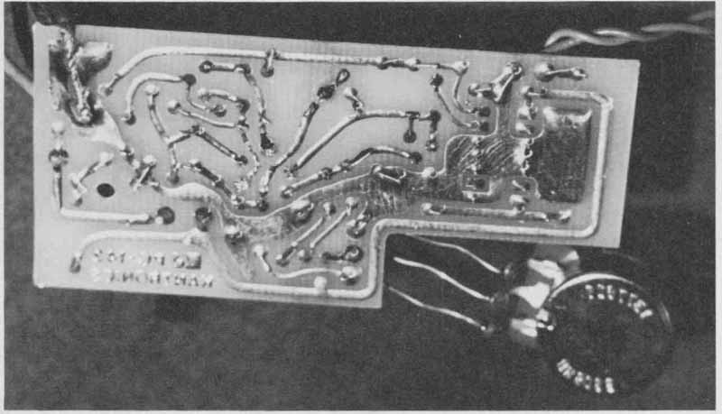
FIG. 9 Foil side of the CB receiver PC board. The shield of the coaxial
cable can be seen soldered to the ground at upper left. Note the larger
wires to the potentiometer at bottom right. These require larger pads
and holes than most of the other component leads. (Photograph: Precision
Arts, Ltd.)
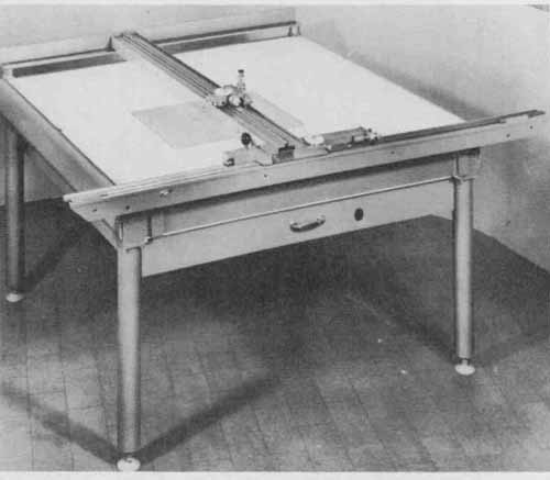
FIG. 10 The coordinatograph is often used for precision drafting of
printed circuits. (Keuffel & Esser Co.)
3 Other Aspects of PC-board Layout and Construction
Orientation of components is important from the production standpoint. FIG. 11 shows in diagrammatic form the PC boai4 moving along the waves of the wave-soldering equipment. The solder just touches the locations on the foil (solder) side of the board where leads from the components go through the board by way of the holes which have been drilled through their pads or lands. This makes small, neat, strong solder connections. In order to minimize unavoidable “bridging” of solder, dual-in-line packages, flat-packs, etc., are positioned with their long dimensions parallel to the direction in which the board moves across the solder waves. This is often the long dimension of the PC board, but that depends on the production equipment and methods in use. (In the additive system of manufacture, the solder bath is not used. Interconnections are formed during the reflow process. If this system is used, the orientation of components to reduce bridging is not important.)
Part of a N/C machine which automatically puts components on a board and clinches them into position is shown in FIG. 12c. This method requires that the pattern be limited to the X and Y axes as shown in FIG. 12a. The components are first placed on tapes in the order in which they are to be inserted on the board. The tape ( FIG. 12b) moves through the machine much as an ammunition belt is fed through a machine gun. Components are then placed on the board one after the other in a line. The idea is to minimize the number of passes that the board and components have to make through the machine.
A semiautomatic insertion machine is shown in FIG. 13. This machine is very suitable for small companies where circuit boards are not complex, or where the number of boards produced is not high. Larger, more expensive, automatic insertion machines are used for PC boards where the density of components is high and production quantities large.
Transistors and capacitors are available with preformed “standoff” leads that facilitate their assembly on the board. Dual-in-line package elements can be mounted directly on the board with their leads projecting through, or they can be separated with a thin spacer to eliminate possible short-circuiting. They can also be plugged into sockets which are fastened to the board as other components are. This facilitates removal and replacement of ICs, microprocessors, etc. Completed boards are often sprayed with a material that inhibits the deleterious effects of humidity, fungus, etc. This is called conformal coating.
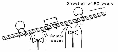
FIG. 11 Dual-wave soldering process. The first wave provides good wetting
of the component leads to the signal paths. The second, more gentle,
wave removes excess solder.
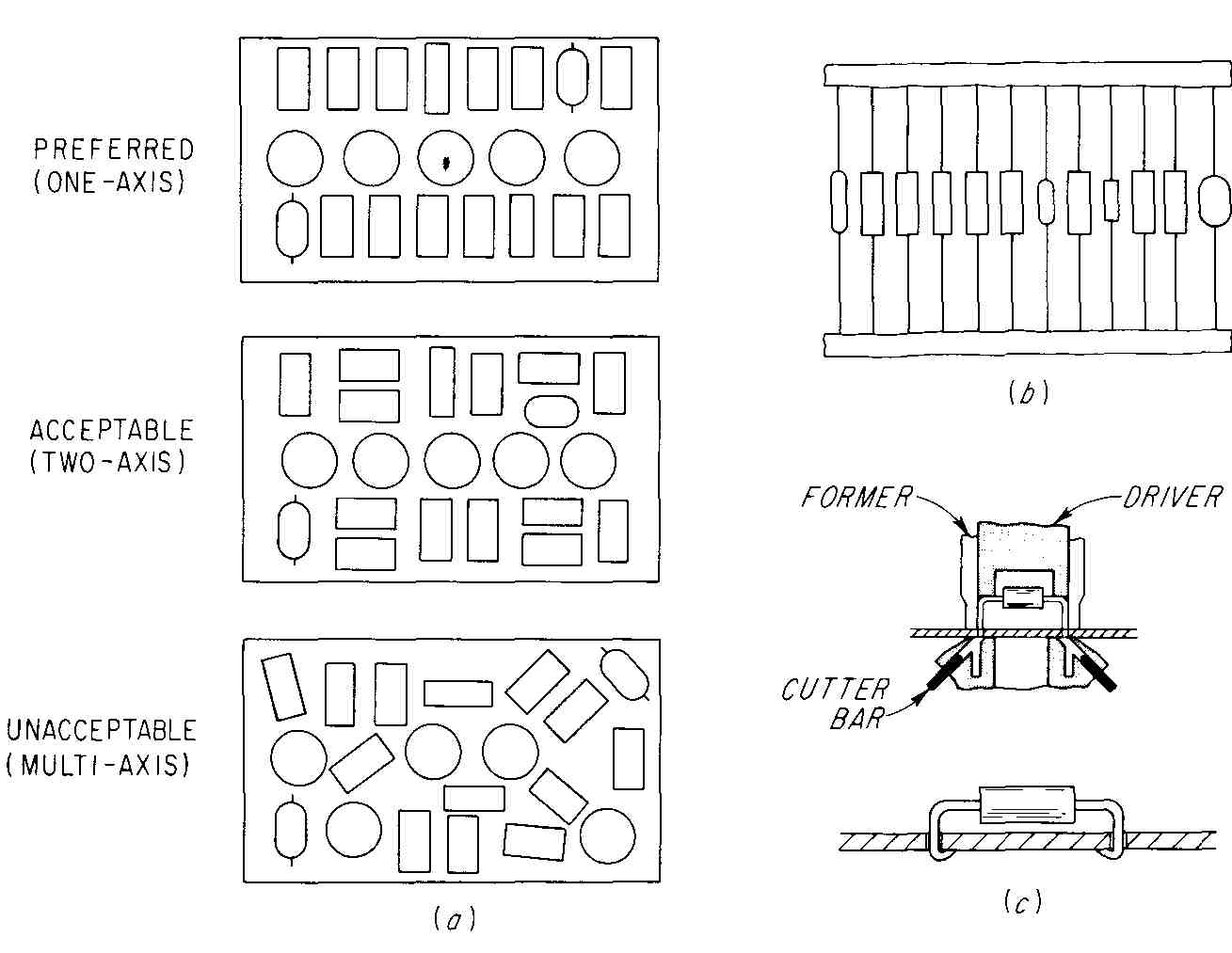
FIG. 12 Orientation of components for automated assembly of PC boards:
(a) preferred and unacceptable designs for automatic assembly; (b) components assembled on tape; (C) section of insertion machine action.
Over a long period of years many devices have been designed and built for use with PC boards. In addition to the sockets just mentioned and shown in FIG. 14a and microprocessor, IC packages, and relays, there are DIP switches ( FIG. 14b) and various displays, some of which are shown in FIG. 1 4c. The vacuum fluorescent display has gained popularity in automobiles because the characters show up well in bright light or darkness, and also because all letters of the alphabet — as well as numerals — can be formed. [ all letters can be formed with a seven-segment light-emitting diode (LED) or liquid crystal display (LCD).]
4 Some Specifications for Good PC-board Design
The following are some minimum design standards prepared by a company that produces thousands of printed-circuit boards a year:
1. All components will be oriented on the X or Y axis wherever possible. Dual-in-line IC packages will be oriented on one axis and keyed in the same direction wherever possible.
2. Components will be mounted on only one side of the PC board.
3. Maximum board size shall be 5.80(147) X 11.70 in. (297 mm), if possible, to allow wave soldering and programmed assembly. (The sizes may vary from company to company, depending on the equipment used. This specification will not apply if the electroplating process is used instead of the solder bath.)
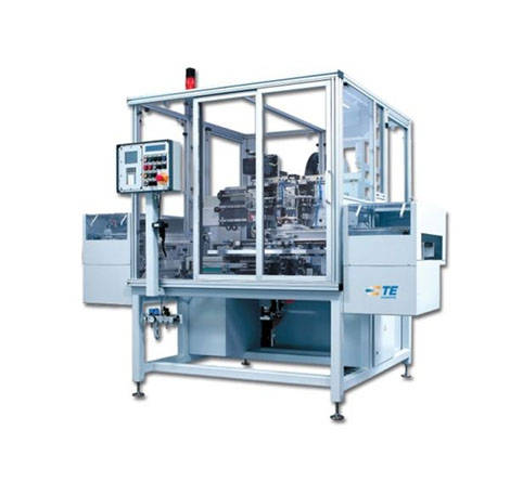
FIG. 13 Insertion machine for PC-board components. With this machine
the operator can quickly position devices onto a board. ( Kansas City
Star.)
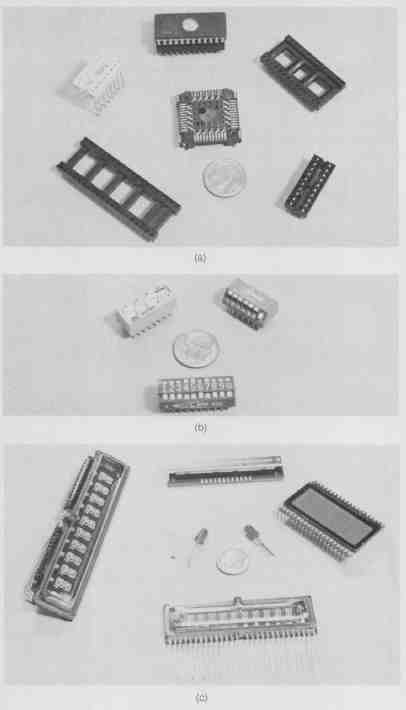
FIG. 14 These items can be mounted on standard 0.10-in.-grid PC boards:
(a) sockets for ICs, with a Chip carrier socket in the center and a programmable
memory (PROM) package mounted on a socket at the top; (b) DIP switches
which have on-off switches 0.10 in. apart; (c) displays, with vacuum
fluorescent displays at left and bottom, LED bar display at top, LCD
display at right, and single LEDs near the dime. (Kantronics, Inc.)
4. Components should be located so any component can be removed from the board without removing any other part.
5. When large areas of ground plane are required, crosshatch or solder mask to avoid excessive buildup and warping during soldering.
6. All boards must have at least two holes referenced to the artwork. These holes, which may be mounting or extractor holes, must be 0.062-in. (1.57-mm) diameter or larger.
7. Component pad centers will conform to standard spacing and should be maintained on even 0.025-in. (0.635-mm) graduations.
8. Minimum spacing shall be maintained, as shown in Table 1 and FIG. 6.
9. Components that dissipate more than 2W should not be mounted on a PC board, but should be heat sunk directly to the chassis.
10. Determine pad size as follows:
a. Maximum mis-registration allowed: 0.002 in. (0.051 mm).
b. Minimum working tolerance: 0.008 in. (0.203 mm).
c. Plated-through holes require a minimum of 0.006 in. (0.153 mm) for through-plating.
d. Allow 0.002 in. (0.051 mm) for etching tolerance per ounce of copper.
e. The above plus the minimum required annular ring multiplied by two for each side of hole.
As an example, we might have a finished hole size of 0.031 in. (0.787 mm), mis-registration 2 X 0.002 for 0.004 in. (0.101 mm), working tolerance 0.008 in. (0.203 mm), through-plating 0.006 in. (0.153 mm), etching tolerance 0.002 in. (0.051 mm), minimum land 2 X 0.005 for 0.0 10 in. (0.254 mm), for a total of 0.061 in. (1.57 mm), which would be the minimum pad size.
11. Component bodies will be at least 0.05 in. (1.27 mm) from the edge of the board.
12. No conductor path shall be closer than 0.025 in. (0.635 mm) to the edge of the board.
13. No component pad perimeter will be closer than 0.05 in. (1.27 mm) to the edge of the board.
14. Conductor paths should be oriented to run parallel to the longest axis on the solder side of the board. (This reduces bridging during wave soldering.)
15. Conductor paths should be oriented to the XY coordinate system. Necessary deviations should be at 45°.
16. All final artwork will be done at a 4: 1 scale minimum. Any board requiring very critical tolerance may be done at 10: 1.
[This is a product design specification. It may or may not apply to PC boards designed by other firms.]
17. Wherever possible the following markings will be added to the component side of the board:
a. Termination numbers or wire colors
b. Polarity for capacitors, diodes, etc.
c. Test-point identification
d. Adjustment identification