AMAZON multi-meters discounts AMAZON oscilloscope discounts
[cont. from part 1]
5. Double-sided and Multilayer Board Layout
FIG. 15 is the schematic diagram of the display-board circuit for a small radar unit. The components consist of three integrated circuits ‘2’ and 13; three cold cathode display lamps DS DS and DS two transistors Q and Q two resistors R and R and a connector J After some analysis of the schematic, an assembly drawing (or component layout) was made. FIG. 16 shows a satisfactory arrangement of the devices. Note that the cathode lamps and integrated circuits are positioned with I close to DS etc. The schematic diagram shows seven connections between I and DS therefore, if they are located close to each other, crossovers will probably be minimized. If one allows space for some circuit paths between the devices and lays out to scale (double, or 2: 1, in this case), the size of the board that results is about 3 (76) X 2 in. (70 mm).
Using this layout, one or more rough sketches of possible circuit patterns have been made. One such sketch is shown in FIG. 17. This was made on a sheet of tracing paper placed directly over the layout of FIG. 16. A logical step is to run ground and power paths where they can conveniently be connected to components. Such a line starts at terminal 9 of DS connects at e of Q and goes to J ground. Other logical procedures are to sketch paths between components in one direction, say, vertically such as between 7 of DS and 13 of ‘2 and between 4 of DS and 14 of ‘2. Note that there are few crossovers in the area between DS and ‘2 on the left and DS and I on the right. Also note that it is possible to have conductor lines going under the ICs and cathodes. This is possible even on the component side because the bottoms of the devices, when mounted, are raised almost a millimeter off the board.
Careful layout and preliminary sketching have not been able to eliminate quite a few crossovers of the radar circuit. This indicates that a double-sided board is the most logical and economic construction. (It is possible to treat a crossover as a component on a one-sided board by making a “jumper” out of wire. But the economics of modern PC-board manufacture suggests that such crossovers be held to a bare minimum.) Therefore it was necessary to make more sketches for the printed paths on the component side and for the printed paths on the other side. One approach is to put all the vertical paths (as in FIG. 17) on one side and the horizontal ones on the opposite side. It usually is not this simple, but this is one way to begin.
The final results of such preliminary sketching are shown in the two master layouts of FIG. 18. Each layout was drawn double size. The distance between pads was 0.2 in. (5 mm). The paths were laid down with 0.026-in. (0.66-mm) tape, and the same figure was used for minimum space between paths. Most paths are horizontal or vertical, but there are some paths in congested areas (between 12 and 1 for instance) where it was necessary to use angled lines in order to meet minimum spacing requirements.
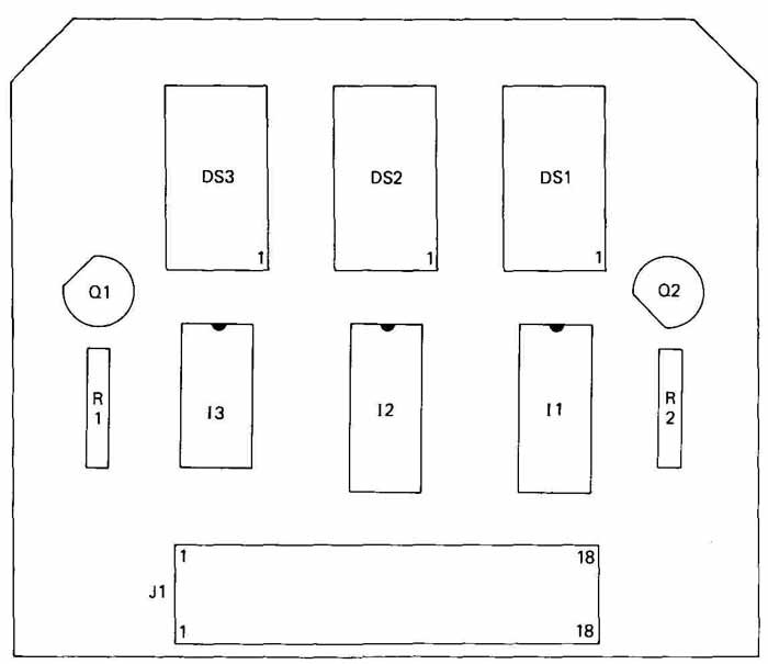
FIG. 16 Assembly drawing (component layout) for hand-held radar circuit
board.
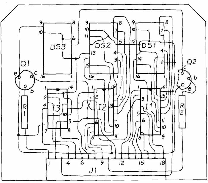
FIG. 17 Preliminary sketch of connections for radar circuit board.
Such preliminary drawings are a link between the schematic diagram and
the master artwork.
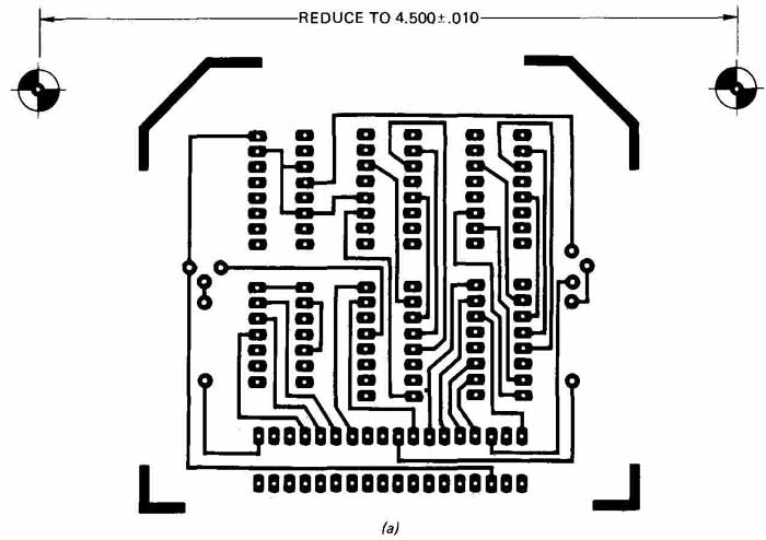
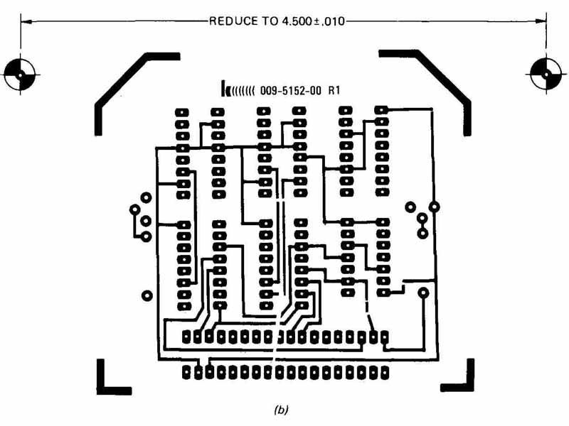
FIG. 18 (a) Master layout for component (near) side of PC board. (b)
Master layout (final artwork) for far side of PC board. (Kustom Electronics,
Inc.)
The master layout must be made on a dimensionally stable medium to a scale larger than the final product. Registration is important, and two (in some cases three or more) registration points quite far apart are required. The two points used in FIG. 18 are such that the small holes in the centers remain white when both sides are exactly aligned with each other. The heavy corner markers establish the board outline on the inside of these markers, as shown in FIG. 19. Lines in the master artwork must be solid black, unless a colored taping system is used. If the color system is used, blue tape is used for conductor paths on the component side and red tape is used on the opposite side. These specially made tapes can both be put on one sheet of clear polyester film. With the use of filters, the photographic process can “hold” one color while “dropping” the other color, and vice versa. Thus two circuit patterns, one for each side of the PC board, can be made from the two-color layout.
Once the master artwork is completed, it can be used to make other drawings, such as the drilling drawing ( FIG. 19), the marking drawing ( FIG. 20), and solder masks. Marking drawings include such items as polarity markings, serial number, vendor’s number, and the name of the company using the board. (Many product manufacturers have their PC boards made by firms that specialize in PC-board production.) Marking drawings are usually made with commercially available adhesive lettering and markings. Care should be taken in locating the markings and lettering so that they are not hidden by the components. Lettering and registration marks should be at least 0.015 in. (0.381 mm) thick, and letters should be high enough to read after reduction to final board size. The number 1 is used to indicate where pin 1 of the IC is to be located. The dashed lines for component outlines are not actually shown.
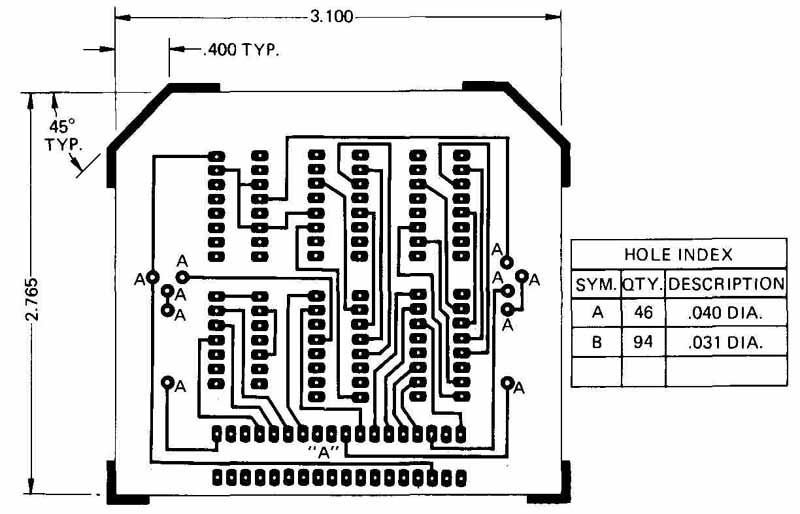
FIG. 19 Drilling drawing for PC board. All holes not labeled A are
B size.
FIG. 20 Marking drawing for a small printed circuit board.
In some cases the identifying number for each component (e.g., R C is put on this drawing and printed on the board. For small components this identification is located so that the device is placed directly over the printing. (Unfortunately the device usually hides the printing, and locating a part for replacement becomes a chore.)
If the density of components (and wiring) that are to be in a circuit is high, two sides of a single board may not be enough to accommodate all the printed circuitry. In such an instance, more than one board may be necessary. A photograph of a multilayer board is shown in FIG. 21. This high-density board with a lot of integrated circuits has four layers of printed circuitry printed on two pieces with a thin layer of what is called prepreg material in between. In the lower right-hand sector, just below the 1 integrated circuit and to the right or left, can be seen three colors (or shades) I lines, which represent circuit paths in various layers. (Unfortunately, only two layers can be seen in the photograph.) Boards with as many as 14 layers have been manufactured. Sometimes a number of circuit boards interconnect with (plug into) such a multilayer board. In these cases such a board is called the “mother” board. FIG. 22 shows a cross section of a six-layer board. After the board patterns have been made from the artwork, they are aligned with precision and the layers of prepreg material are placed between the boards. Then the assembly is placed in a heated press under high pressure. A six-layer board made of three 0.012-in.-(0.30-mm-) thick laminates might have a total thickness of 0.062 in. (1.57 mm), including substrate, prepreg, and thicknesses of printed wiring.

FIG. 21 Photograph of a four-layer PC board. At least two layers of
conductor paths can be seen in the lower right sector. (Kustom Electronics,
Inc.)
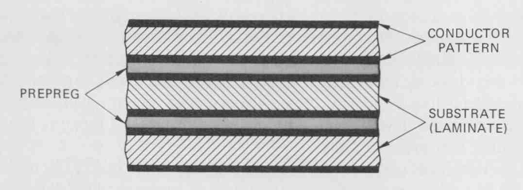
FIG. 22 Cross section of a six-layer circuit board. Total thickness
is about 0.062 in. (1.57 mm).
The design and layout for multilayer boards is beyond the scope of this guide. Considerable experience is desirable. For one thing, a decision must be made about which circuits are to be placed in which layers. Sometimes ground planes and voltage buslines are the only items in a single layer. Accuracy of registration and manufacture are very important. Computer-aided layout is often used.
Photographs of another double-sided PC board are shown in FIG. 23. Approximately 150 electrical components are on this 5.75 X 6.75 in. board. One memory device, U has been programmed by the manufacturer and has a note to that effect pasted on top. This computer-transceiver interface (for amateur radio operators) has an operator’s manual that includes a schematic diagram and component layout (placement diagram). The printing from the latter drawing shows up on the board itself. In FIG. 23 such lettering as U U, U and C is visible. However, identification of most resistors is hidden by the resistors themselves. For this reason, the operator should have the component placement diagram, for troubleshooting.
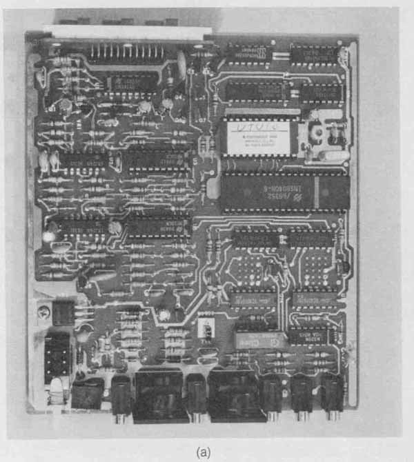
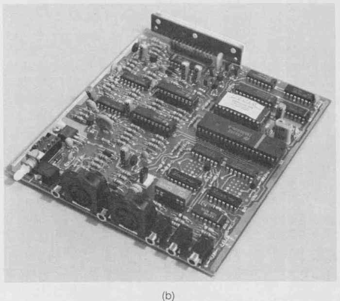
FIG. 23 Photographs of a PC board for a computer-transceiver interface
unit: (a) looking down on component side; (b) viewing at an angle, with
connectors on one edge near bottom. The back side of a LED bar display
is shown at the top.
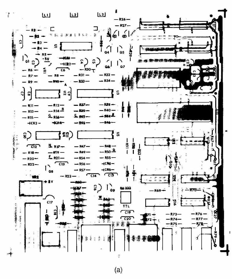
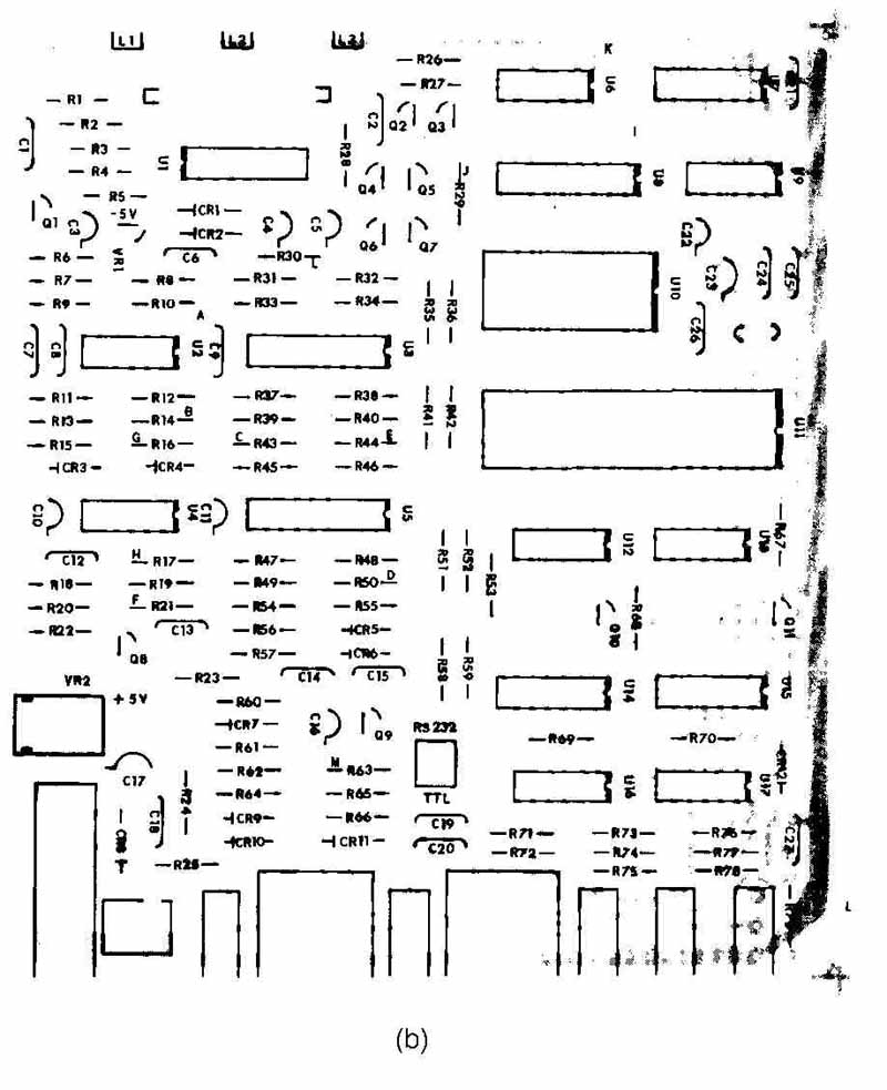
FIG. 24 Two of four photographs of the transceiver interface board:
(a) component side showing markings for small components and outlines
for IC packages and a few other devices—circuit paths shown are on the
same (near) side; (b) x-ray photograph of the component side, showing
the PC paths of the far side. (Kantronics, Inc.)
A recent development in photography has made it possible to make a single photograph of a board that shows the components on one side and the printed wiring on the opposite side. FIG. 24 shows two photographs of the PC board in FIG. 23. FIG. 24b shows the outlines of the ICs and identification of the smaller devices as seen looking down on the component side of the board. But the printed wiring is that of the other side. This is called an x-ray photo. Two other photos were made looking at the other side of this PC board but are not shown. One is an x-ray view in which the printed circuits of the component side show through. These photographs are useful to the designer and production personnel, but are also reproduced and sent to the users of products. They are very helpful to whoever has to replace a part or perform modification.
6 Surface-mounted Devices
We have shown a few surface-mounted devices in Figs. 3-28 and 3-35. Surface mounting has already begun to change many aspects of electronic assembly. A whole family of tiny active and passive’ devices is being developed to meet the demand for lighter, smaller, cheaper, and better boards. These components are soldered to board solder pads which are matched to the “footprints” made by the leads of the package. Through holes are eliminated, and the proper mix of active and passive components cuts the length of leads, thus reducing parasitic capacitance and inductance in the wiring. Such technology is producing smaller, denser, and cheaper boards whose high-speed ICs can operate at optimal efficiency.
In FIG. 25a we have shown a section view of a PC board having pin-type and leaded-type components mounted in through holes and soldered on the bottom (foil) side of the board. In FIG. 25b a chip carrier is shown with J-type leads and a small outline package with gull wing leads soldered onto a board. The J and gull wing leads produce a rectangular “footprint,” and the PC drawings and final artwork have pads whose rectangular shapes match the footprints. Widths of lines and spaces between lines have become smaller. Line widths now in use are 6 mils (0.006 in. or 0.15mm) to 12 mils (0.012 in. or 0.30 mm) wide, and minimum line spacing is about equal to line widths. FIG. 26 shows the lands or pads and 10-mil lines of a small part of the final artwork for a circuit containing small-outline integrated circuits (SOICs) and the outline and end view of a 14-pin SOIC. Standard dimensions are being developed for 14-, 24-, and 48-lead SOICs. Standard 3- and 4-lead small-outline packages, called SOT 23 and SOT 143 for transistors and certain other devices, are 114 X 51 x 43 mils. New equipment has been developed for production of small-outline PC boards. Two soldering methods are used: (1) reflow in which components are placed over solder that has been screened over the pads and then is heated and melted and (2) dual-wave soldering in which the devices are exposed to two soldering procedures for 2 s each.
1. An example of an active device is a transistor. Examples of passive devices are resistors and capacitors.
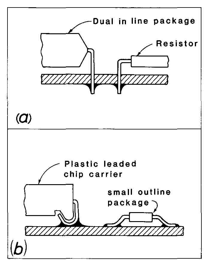
FIG. 25 The old and the new. (a) Through-the-hole mounting of leaded
components. (b) Surface mounting of chip carrier with J-shaped leads
at left, and small- outline IC package with gull-wing leads, right. (Reprinted
from Electronics, February 9, 1984)
A circuit board with surface-mounted devices is shown in FIG. 27, and in the center part of FIG. 28, with two other boards. This 3.75-in. (95-mm) X 2.25-in. (57-mm) unit is part of a portable transceiver. It has more than 200 active and passive devices mounted on both sides. These can be identified by their shapes and colors, not all of which (especially browns and grays) show up well in the accompanying photographs. The colors and devices are:
- White Resistors
- Silver Semiconductors (metallic)
- Black Integrated circuits and electrolytic capacitors
- Brown Capacitors
- Gray Capacitors
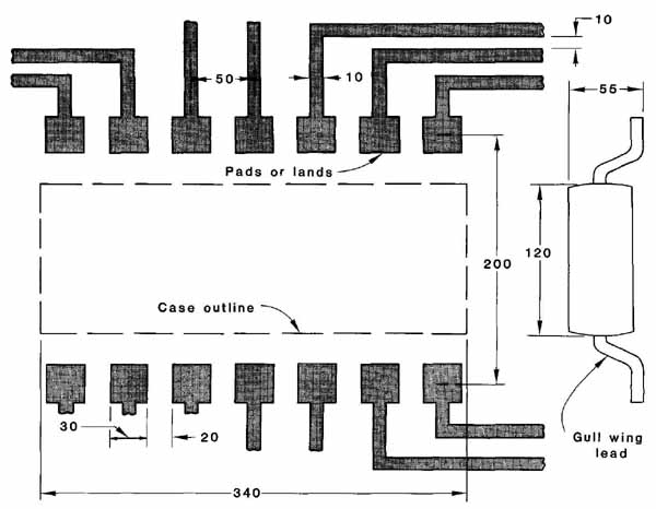
FIG. 26 Outline and end view of small-outline integrated circuit and
small portion of PC artwork for surface-mounted components. Dimensions
are in mils (1 mil = 0.001 in.).
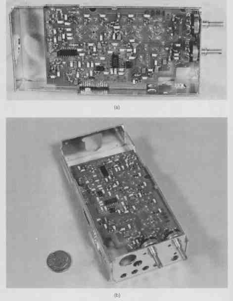
FIG. 27 (a) and (b) Two views of a circuit board having surface mounted
components. (King Radio Corp.)
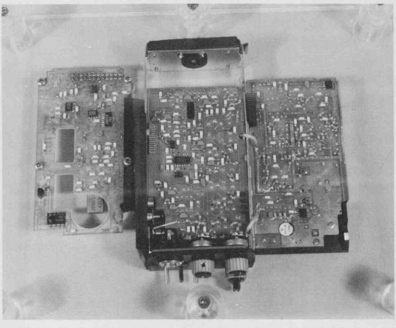
FIG. 28 A view of a transceiver in which the circuit board of the previous
photograph is mounted with two other boards having mostly surface-mounted
devices. (King Radio Corp.)
Two SOICs can be seen with their gull-wing leads projecting away on each side. On either side and close to one IC are two black electrolytic capacitors. White resistors are easy to see. Brown and gray capacitors, nearly square in shape, appear gray in the photograph and are not as plainly visible as the black-and-white devices. In FIG. 27a a SOT 23 transistor is shown just below the black capacitor, which is to the left of the IC whose long dimension is perpendicular to the long dimension of the board (and chassis). The SOT, which is silver-metallic color, shows up as gray in the photograph and has two leads above and one below. Printed-circuit paths are also visible in several places in FIG. 27a.
The general layout and drawings for boards with surface-mounted components are much the same as those for PC boards of recent years. One might expect the following differences:
1. Larger scales
2. Narrower paths
3. Smaller parts
4. Closer spacing
5. Different pads
6. Greater density
7. More components (on both sides if necessary)
8. No, or fewer, through holes
9. 50-mil grid spacing
Surface-mounted technology is one of the waves of the future. However, PC boards using present state-of-the-art components with 100-mil spacing will be manufactured and used for many years to come.
7 Mounting of PC Boards
Printed-circuit boards are attached to a chassis in various ways. The method is determined by the size and shape of the board, the size and shape of the chassis, grounding and other electrical requirements, ease of removal if such is desirable, ventilation requirements, and the standard procedures used by the manufacturer.
The three figures starting with FIG. 29 show three different chassis. The accompanying printed matter describes briefly how the boards are attached. Figure 29a is the case (and chassis) for the transceiver interface unit shown in Figs. 23 and 24. The 5.75-in. (146-mm)-wide board is simply slipped into the case with two edges sliding along, and in, the grooves on each side. After front and rear panels are put in place, the black end frames are pressed on (with a tight fit), completing the assembly of this 1.90-in (48-mm) X 5.90-in. (150 mm) X 7.00-in. (178-mm)-deep unit. The case-chassis is made of extruded aluminum. The finished unit is shown in FIG. 29b.
The boards shown in FIG. 30 are fastened onto the chassis with 2-56 screws (No. 2 screws having 56 threads per inch). This chassis is made of cast aluminum. Tapped holes can be seen on its top edge. One of several features of this KT 79 transponder is a double-tuned coaxial line filter near the lower left corner. Near the bottom of the picture, U-shaped coupling probes transmit the signal from the circuit board at the right through the filter and out through the small board at the left.
The photograph of the Heathkit robot in FIG. 31 shows three of the 13 circuit boards. The large CPU board is fastened on to the square “wrap around” aluminum chassis by means of No. 6-32 screws and nuts and 0.30-in. (8-mm)- long spacers between chassis and board. However, the two smaller boards are “pressed” onto plastic “bayonet”-type fasteners which go through the small holes with a little pressure and hold the boards firmly in place. The spacers for these boards are plastic. Approximately five PC boards are mounted on the other two sides of the chassis, while the rest of the boards are in various places. One is located under the hexadecimal keyboard, which is visible at the top.
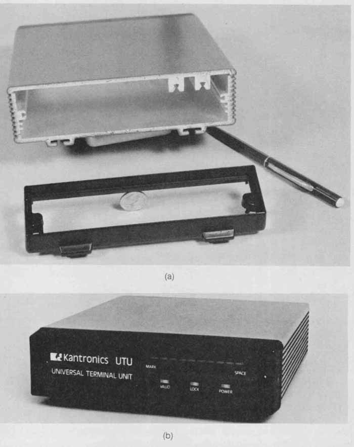
FIG. 29 Case and chassis for the UTU transceiver interface unit: (a)
empty case with the front parts removed; (b) the complete unit. (Kantronics,
Inc.)
The flexible board for the calculator shown in FIG. 2 has two small holes near each end of the LCD display which is at the right in the photograph. (One hole can be seen on the flexible board above the display and one can be seen “below” the display.) These 0.08-in. (2-mm) holes are pierced by small plastic pins on the bottom part of the calculator case when the circuit board is placed between the top and bottom parts of the calculator, and these parts are pressed together. The flexible board is also clipped to the inside half of the keyboard, which fits below or underneath the keys of the keyboard. Thus the board is held in place by the two pins and the clips and the fact that its shape exactly fills the space that is available.
These are some of the ways that boards are attached or mounted. There are other ways which we haven’t covered. Designers and detailers must know how a board is to be attached before the final artwork is done.
SUMMARY
Printed-circuit board technology is a mature one, but changes are still occur ring. In the original boards the components were mounted on one side and the printed circuits on the opposite side. Now, in many boards the components are mounted on one side and PC paths on both sides. It is also possible to have components and printed circuits on the same side. In the future, some boards may have surface-mounted devices on one side, present state-of-the-art components on the other side, and printed wiring on both sides. Printed-circuit technology is such that the density of components and circuit paths may be high enough to require multilayer boards.
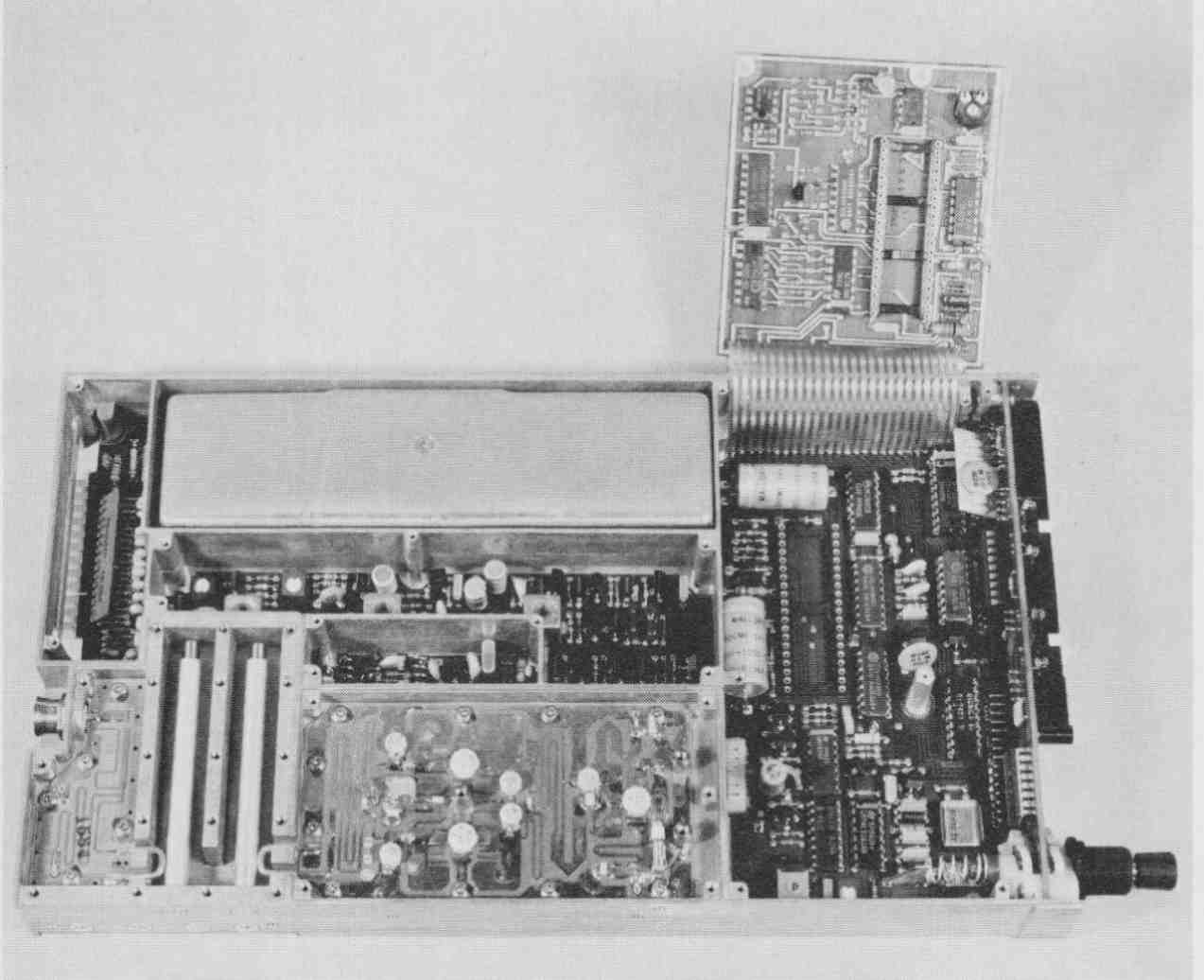
FIG. 30 The chassis for a transponder for aircraft. This cast aluminum
chassis holds several circuit boards and some other parts. (King Radio
Corp.)
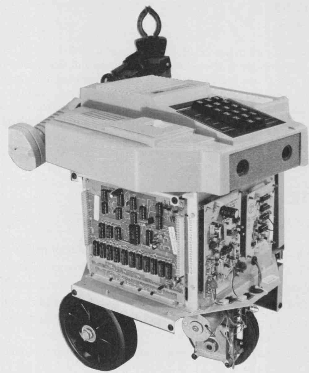
FIG. 31 Photograph of the Heathkit robot with side panels removed.
Three of its 13 PC boards are visible.
Artwork for PC boards must be accurate and therefore is often drawn two or four times the size of the finished conductor pattern. It may be done in ink on a stable medium such as Mylar, or with tape and preprinted pads, bends, etc. Companies that make or use PC boards usually have extensive lists of specifications that must be followed by the drafter or designer. Some of the drawings that are often included in the production of a PC board are:
1. Preliminary sketches for component location and conductor paths
2. Component layout
3. Master layout, final artwork
4. Drilling drawing
5. Marking drawing
6. Solder mask
Many scales are in use for PC-board layout. Both 2: 1 and 4: 1 are common. Some computer-assisted drawings are drawn full size. Scales of 10: 1, 20: 1, and 100: 1 have been used. Printed-circuit paths are often drawn horizontally or vertically. Sometimes electrical requirements, such as resistive pinching and inductive coupling, dictate what directions adjacent lines should go. Production methods and economics (minimum use of materials) also must be considered in circuit-board layout.
QUESTIONS
1. What drawings may be required for the production of a rather complex PC board?
2. What are some typical widths for printed-conductor paths?
3. What are some typical scales used in making master layouts?
4. What grid spacing is being used for surface-mounted devices?
5. What is the first step in making drawings for a printed circuit?
6. Show, by means of sketches, the following: eyelet, board outline, pad, elbow, and registration mark for use in PC-board construction.
7. What is the purpose of putting a socket on a PC board, and then inserting an IC into that socket?
8. What information is included in a marking drawing?
9. Where is a good place to show the number of a resistor on a PC board? Show by means of a sketch.
10. Where is the outline of a PC board in relation to the heavy corner markers?
11. What is the difference in the pad shape for, say, an IC on a typical PC board and the pad shape for a PC board having surface-mounted components?
12. What is the purpose of a solder mask in PC-board production?
PROBLEMS
1. The completely dimensioned working drawing of a small PC board appears in FIG. 32. Using a scale of 1 in. = 0.30 in., draw this board on an 8 X 11 or 9 X 12 sheet. Your instructor may specify a completely dimensioned drawing with or without lettering, a drilling drawing, a marking drawing, or a combination drilling-marking drawing. (An optional fin. = 0.10-in, scale will require the use of a 9 X 12 or 11 X 17 sheet.)
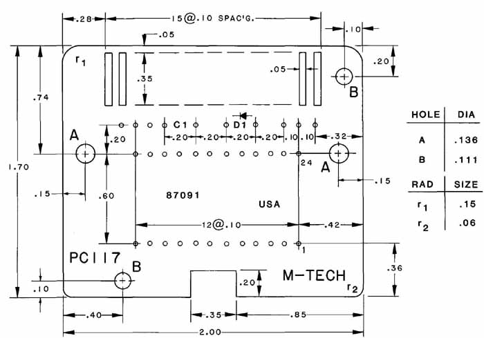
FIG. 32 ( Prob. 1.) Detail drawing of a small PC board.
2. The artwork for the foil side of the PC board for Prob. 1 is shown in FIG. 33. Make a scale drawing to 1 in. = 0.30 in., 4: 1, 5: 1, or in. = 0.10 in. of the master layout for this board. Use line widths of 0.015 or 0.020 in. for the thin conductor lines, or heavy pencil or ink lines if you do not have tape. The (shaded) ground plane should be about as shown and may be within 0.030 in. from the edge of the board. Add registration marks and any other items your instructor may request.
3. The dimensioned drawing of a PC board is shown in FIG. 34 with the PC paths on the component side. Do one or more of the following at your instructor’s request: (a) make a drilling drawing using 0.03-in. (7.6-mm) holes; (b) make a marking drawing showing all lettering; and (c) make a final artwork drawing for the PC paths for this side using line widths of0.015, 0.02, or 0.03 for the narrow lines and 0.05 for the wide line. Do not show pads for the ICs unless you have the appropriate appliqués. The addition of pads to those holes that are joined to printed-conductor paths at C and C would be quite appropriate.
This problem will barely fit on an 8.5 X 11" sheet if a scale of 1 in. = 0.30 in. is used. A 3/8 in. = 0.10-in, or 5: 1 scale (1 in. = 0.20 in.) will require the use of a 11 X 17 sheet.
4. Draw the 2 X 2 in. circuit board shown in FIG. 33b to four times
actual size. Then complete the location of the components for the schematic
diagram shown in FIG. 35a. Show the necessary wiring (as hidden lines
on the other side of the board) to agree with the schematic diagram.
Add notes as required by your instructor. An alternative solution would
be to draw a mirror im
age of the board and put the components in as hidden
parts and the wiring in as solid. Use 11 X 17 or 12 X 18 paper. Typical
component sizes are: resistors, 0.14 X 0.30 in.; capacitors, 0.20 X 0.80
in.; and transistors, 0.37 in. in diameter. This can also be used as
a PC-board layout problem.
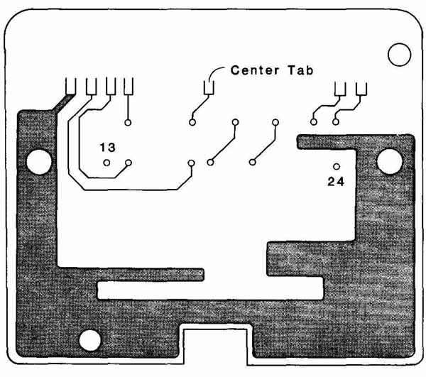
FIG. 33 ( Prob. 2.) Foil side ol PC board No. 117 with printed wiring.
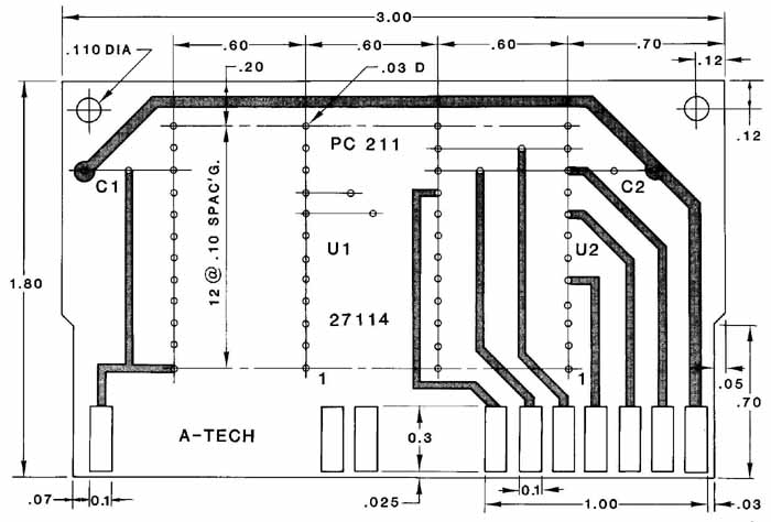
FIG. 34 ( Prob. 3.) Detail drawing of PC board No.211. The wiring of
the component side of this board is also shown.
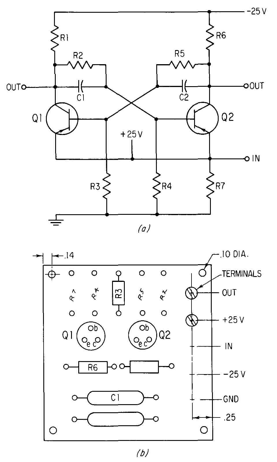
FIG. 35 ( Prob. 4.) Schematic diagram (a) and suggested layout (b)
for a wiring or PC-board layout.
5. FIG. 36 shows a preliminary layout of a circuit board that is to contain the sweep-generator circuit. Check the layout against the schematic diagram (no dot system) for improvement in layout. Make a PC-board master layout (outside dimensions are 2.20 X 2.40 in.) to a 4: 1 or 5: 1 scale. Use the 0.10-grid system for locating components whose sizes are: resistors, 0.25 X 0.09 in., except R is 0.375 X 0.09 in.; capacitors, 0.422 X 0.135 in.; L 0.400 X 0.15 in.; and diode, 0.275 X 0.105 in. maximum. Use 0.062-in. conductor paths, with 0.031-in, minimum spacing unless your instructor specifies otherwise. Use 8- X 11 paper.
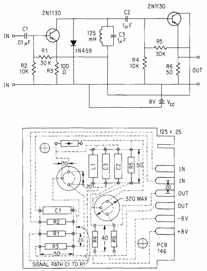
FIG. 36 ( Prob. 5.) Schematic diagram and preliminary component layout
of a circuit board for a sweep generator.

FIG. 37 ( Prob. 6.) Schematic diagram of a timer reset. Major dimensions
of the components are shown below.
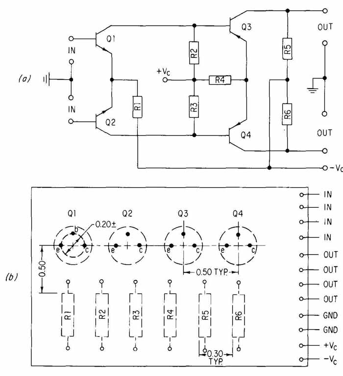
FIG. 38 ( Prob. 7.) A printed wiring problem for a differential-amplifier
circuit.
6. A digital timer circuit is shown in schematic form in FIG. 37. Make a preliminary wiring sketch, a component layout sketch, and a final artwork for a PC board for this circuit. Have all the inputs located at one side with fingers 5.08 mm (0.20 in.) apart. Use a 2.54-mm (0.10-in.) grid. Let conductor paths be 1.57 mm (0.062 in.) wide with a minimum spacing of 0.80mm (0.031 in.) between paths and outside paths and edge of board. Shape and size of board are to be determined by student or instructor, as is scale. Terminal pads are to be 3.18 mm (0.125 in.) in diameter with holes 1 mm (0.040 in.) in diameter. The DIPs, however, will use standard pin spacing of 2.54 mm (0.10 in.). Dimensions of the components shown are in millimeters. Jumpers are permitted.
7. FIG. 38 includes an elementary diagram and a suggested arrangement of parts for a differential amplifier. Make a scale drawing of the final master drawing for the pattern. A maximum of four jumpers will be permitted. The lower figure shows the wiring side of one arrangement of components. Transistor diameters are 0.360 ± 0.0 10 in., and resistor dimensions are 0.093 diameter X 0.375 in. Try to get an acceptable pattern on a board that is no larger than 3.00 X 2.00 in. Freehand preliminary sketches are suggested. If you cannot get an acceptable pattern with the suggested arrangement of components, make your own arrangement. Hole diameters are 0.032 in. Terminal pads are 0.125 in. across. Use 0.062-in, conductor paths with 0.031-in, minimum spacing. Show registration marks and pin no. 1 (top pin), and label the board PCB 46. If you do not have tape, you may be asked to draw the signal path in a single heavy line or two parallel lines. Use 8 X 11 paper. Show one critical dimension.
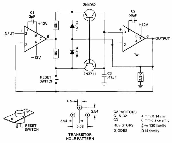
FIG. 39 ( Prob. 8.) A video peak detector circuit. Major dimensions
of most of the components are shown below.
8. FIG. 39 shows the schematic diagram of a video peak-detector circuit. Dimensions of the components are shown in millimeters. Make a sketch of a physical arrangement of components that will accommodate a printed circuit on a minimum-size board. The switch will be attached to the board by wires. It will be mounted elsewhere. Then draw a master layout using conductor path widths of .787 or 1.02 mm, except for a wider + 12 path. Use a scale of 2: 1 for 8.5 X 11 paper or 4: 1 for 11 X 17 paper. Make pads 1.58 mm in diameter with 0.64 mm-diameter holes, except for leads to switch, which will require larger holes. Refer to Table 1 for sizes of components. Jumpers permitted.