AMAZON multi-meters discounts AMAZON oscilloscope discounts
A primary drawing is one that shows the function of a circuit or a system in a logical manner. It is usually the first drawing sketched by an engineer or technician. The primary drawing in electronics and industrial control used to be the schematic diagram. But the ascendancy of digital electronics has necessitated that the logic diagram become the primary one, and this is also true for some areas of industrial control. As systems become more complex or miniaturized (using LSI — large-scale integration — components, for example), the block and flow diagrams are becoming more popular and necessary for the explanation of the functions of these systems.
1 Examples of Block Diagrams for Electric Circuits and Systems
Such a diagram may be used to show the operation of a large electronics system. In such a case, a block would represent a complete and removable chassis, such as a preamplifier, a multivibrator, or even a television camera.
However, in a different situation, a block diagram may be used to facilitate the understanding of a radio receiver or a multistage amplifier, for example. In this case, each block would represent a stage. This is the case of the diagram shown in FIG. 1. At this time it might be a good idea to define the word stage. A stage is considered to be that part of a circuit which includes the main device (e.g., transistor, diode, or tube) and the associated devices that go with it, such as biasing resistors, load resistor, voltage dividers, and capacitors. In other words, a circuit may have several stages, hooked together somehow, so that the signal goes first through one stage, then through the next, and so on. Each block represents a major subsystem. The diagram shows major signal and data paths, inputs, outputs, and control points.
FIG. 1 shows how easy it is to understand a circuit’s operation by means of a block diagram. It is clearly shown that the signal comes through the antenna (usually portrayed by a symbol rather than a block) and then progresses through the mixer circuit, through the intermediate-frequency (IF) stages, and finally to the output stage and speaker. The oscillator, which is an auxiliary circuit, is appended to the main circuit; and, because it is a frequency generator, its output is fed into the signal train as shown by the arrow. A feedback circuit, labeled AGC for automatic gain control, is correctly drawn below the main circuit. If it were desirable to emphasize the AGC circuit, however, it would be appropriate to place it above the main circuit. The purpose of automatic gain control is to prevent fluctuation in speaker volume when the radio signal at the antenna is fading in and out.
2 Preparation of Block Diagrams
A block diagram may use standard symbols for certain elements, but it is predominantly one of blocks (usually, but not always, squares or rectangles). The layout can be facilitated by (1) using freehand sketches in the initial stages, (2) using cutout cardboard blocks of appropriate size and experimental arrangement until the best pattern is achieved, or (3) using cross-ruled paper for an undergrid, thus facilitating the construction of blocks of equal size and uniform spacing between blocks. The size of the rectangles is usually determined by the lettering that goes in them; and, since they are usually drawn about the same size, the block with the most lettering will often set the size of the blocks in the entire diagram.
From FIG. 1 and other diagrams in this section, certain facts about block diagrams can be deduced, and the following rules for their construction can be listed:
1. The signal path should be made to go from left to right, if possible. In large, complex drawings, the input should preferably be at the upper left and the output at the lower right, if possible.
2. Blocks are usually drawn in one of three shapes: rectangular, square, or triangular. (The triangle represents different items in different types of diagram. There are also other shapes for certain specialized diagrams, as will be shown later in the section.)
3. Once the size and shape of a block are determined, the same size and shape should be used throughout the drawing. The size of a rectangle, for instance, bears no relation to the importance of the component(s) it represents.
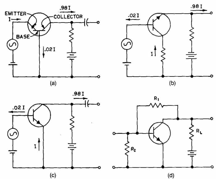
FIG. 1 Block diagram of a typical transistor radio receiver circuit.
4. A single line, preferably heavy, should be used to show the signal train from block to block. In complex circuits or systems, however, more than one line may have to be drawn leading into or away from a block.
5. Arrows should be used to show the direction of signal flow.
6. Some components, usually terminal ones such as antennas and speakers, are shown by means of standard symbols rather than by blocks.
7. Titles, or brief descriptions, of the components or stages represented should be placed within the blocks.
Aside from the above-listed rules, no standardized procedure exists for the preparation of block diagrams. In FIG. 1, for instance, either square or rectangular blocks could have been used. The arrows, which are shown touching the blocks, could have been placed midway between the rectangles if desired.
FIG. 2 shows the control system for an existing coal-fired electric generating plant to which an addition has been made. The addition is a central collector system in which large mirrors (heliostats) track the sun and beam its reflection to a central receiver that converts this heat to steam which goes to the new steam generator or to storage. This diagram differs from FIG. 1 in that the blocks are not all the same size (widely different amounts of lettering), most of the signal paths are bidirectional (arrows at both ends), the master control has a border, and the signal interface (a secondary consideration) is indicated in the dashed lines.
FIG. 3 shows the block diagram for a digital watch. Not shown are the batteries (2) and light-emitting diodes (LEDs). Practically all the circuitry is on a single chip. A three-view photograph of a transparent module without batteries is shown in FIG. 4. Laying out a block diagram for a fairly complex arrangement requires considerable planning, and possibly some experimentation, in order to achieve a neat, well-spaced arrangement of blocks and signal paths.
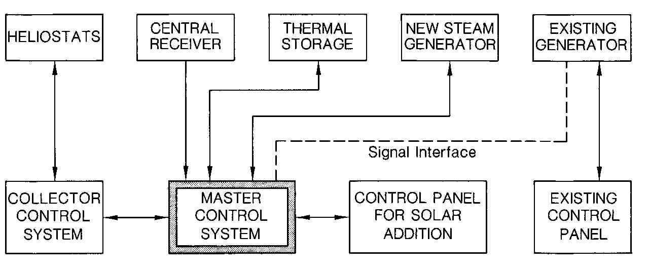
FIG. 2 Flow diagram of the control system of a solar central receiver
system. (Black & Veatch, Consulting Engineers.)
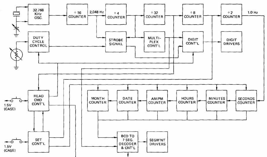
FIG. 3 Flow diagram of a digital watch.
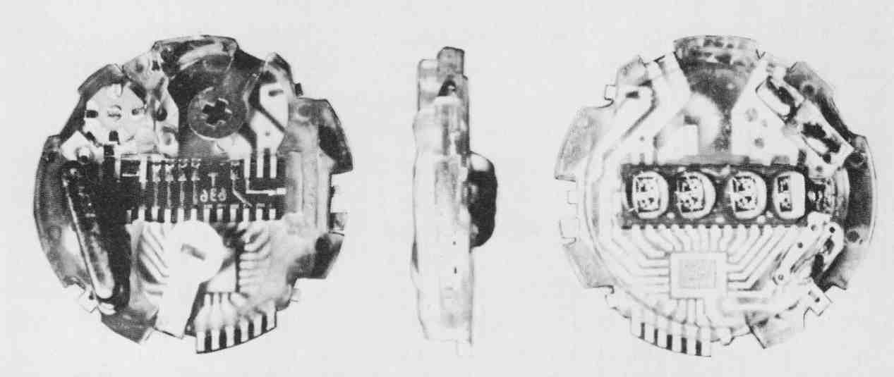
FIG. 4 Three views of digital watch module. In view at right can be
seen the four LEDs and the IC below them. In view at the left can be
seen the contacts for two batteries, the adjustable capacitor (upper
left), and the 32,768-Hz quartz crystal oscillator (near left edge, inclined
at 75°).
3 Microprocessor Diagrams
Microprocessors, which are playing and will continue to play an important role in our lives, require flow diagrams that are somewhat different from those shown previously. This is largely because of the many elements which are connected to the internal data bus that is bidirectional. FIG. 5 is a flow or block diagram of a generalized microprocessor used for instructional purposes. The arithmetic logic unit (ALU) performs the data processing, arithmetic, and similar functions. The accumulator (ACC) is a special register that can store one data word. When the ALU adds two data words, one of the two words has been placed in the accumulator. The result of the addition is then placed in the accumulator. Some of the other registers shown in FIG. 5 are the status register, the temporary register, the instruction register, the A and B registers, and the memory address register. Our drawing shows the registers and other elements with their relationship to the internal data bus. This bus, which moves data words (usually 8, 16, or 32 bits per word), is connected to all the registers, most of which can either place data on or receive data from the bus.
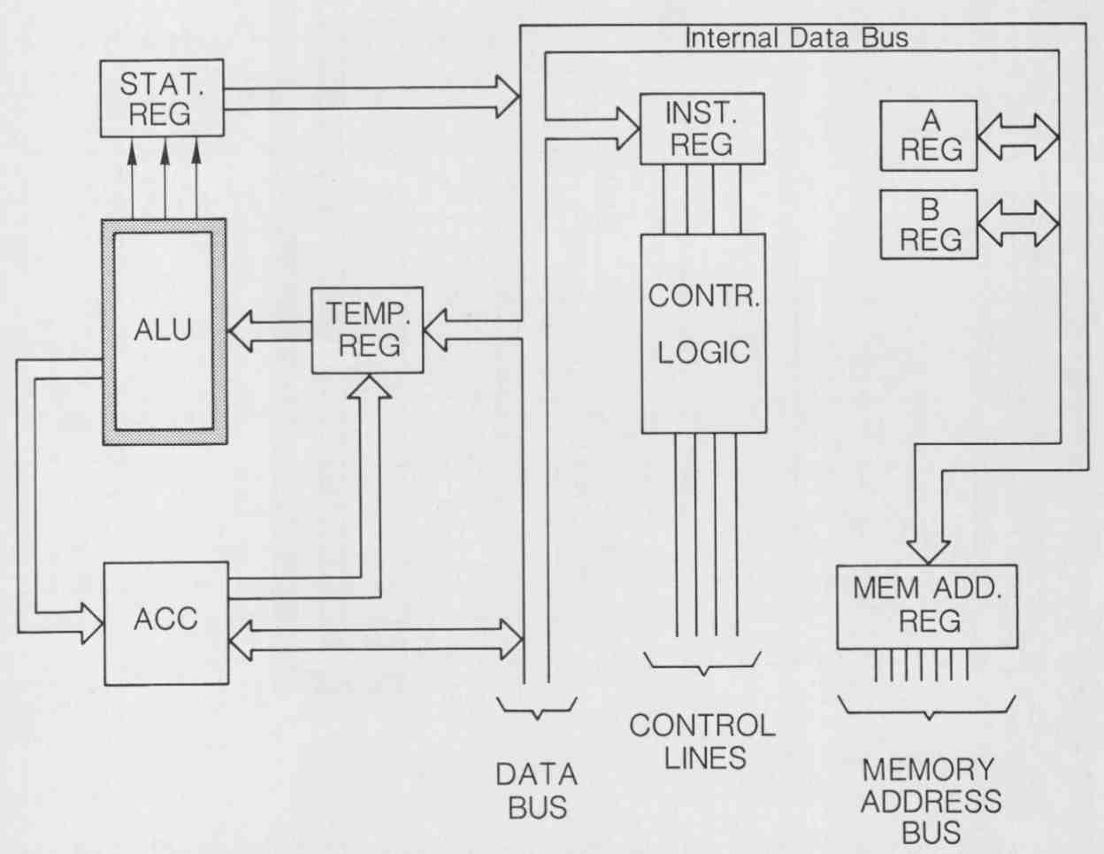
FIG. 5 Block diagram of a microprocessor. The data bus, which is bidirectional,
moves data words in either direction.
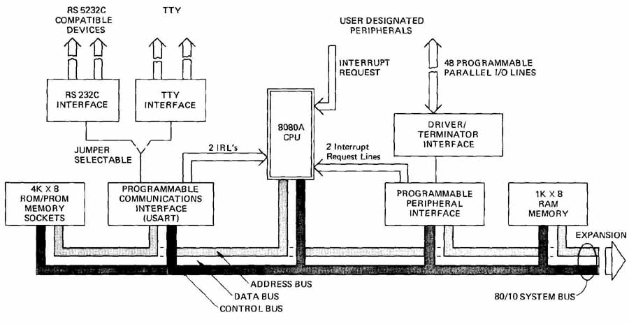
FIG. 6 Flow diagram of the SBC 80/10 single-board microcomputer. (Intel
Corp.)
Before a logic function can place data on the bus, the function must wait for a signal from the control logic. The control signals are not usually considered to be part of the bus. Neither are address signals. For this reason some microprocessor diagrams show control and address buses. FIG. 6 is such a diagram. This diagram is for a microcomputer [ board having a microprocessor and additional integrated circuit (IC) chips] but is similar to a microprocessor drawing. Here, each of the three buses is shown. Some diagrams show just the address bus and the data bus. FIG. 7 is the diagram for a learning device consisting of individual elements of a microprocessor. Such learning modules assist programmers in learning microprocessor concepts. The modules consist of the following:
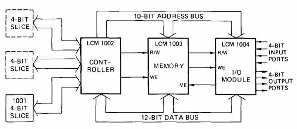
FIG. 7 Flow diagram for the interconnection of microprocessor modules.
(Texas Instruments, Inc.)
4 Logic Diagrams
Beginning with computer design in the 1950s, engineers and manufacturers began to work with logic functions which could be performed by basic circuits. Now people working in many areas—transportation, industry, and communications, for example — find it necessary to make and read drawings that contain symbols representing logic functions. We will describe some of the basic logic functions in this section. However, examples will also appear in other parts of the guide as various circuits and designs are presented.
The symbols that have been used to represent these functions in the past have not been very well coordinated and standardized. For example, FIG. 8 shows six symbols that have been used to represent the AND function. Fortunately the most recent standard, ANSI/IEEE Y32E, has included the revised versions of ANS Y32. 14(1973) and the IEEE and Military Standards that relate to logic symbols. Hopefully they will be accepted by everyone who works with these symbols so that only the distinctive and rectangular shapes will be in use. Inasmuch as the distinctive shapes are quicker to follow, they are widely used, and we shall use them for most of our examples. Figures 9 and 10 show the distinctive shapes for the more commonly used functions. As is the case with other symbols, no exact size has been specified. However, the authors have noted that if the units that are specified in FIG. 10 are drawn as millimeters, the symbols will be just about the right size for most large-size drawings.
Now for a description or definition of the functions. AND: If a signal is impressed at A, and at the same instant a signal is impressed at B, there will be a definite output signal at C. The “high” signals are often referred to as the 1 -state or the ON-state, and the “low” signals are often referred to as the 0-state’ or the OFF-state. Hence, the truth (logic) tables in FIG. 9 show the numbers 1 and 0. [The number zero.]
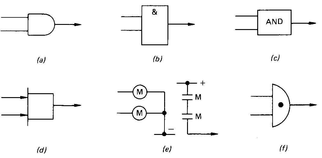
FIG. 8 Graphical representation of the AND function or gate (a) ANSI-IEEE-approved
distinctive shape symbol; (b) ANSI-, AIEE-, and IEC-approved rectangular
symbol; (C) old symbol; (d) NEMA symbol; (e) JIC symbol; (f) old distinctive-shape
symbol. Symbols a and b are recommended.
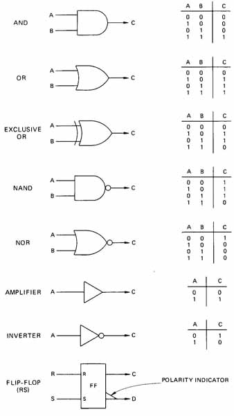
FIG. 9 Distinctive-shape symbols approved and recommended by IEEE and
ANSI. Truth, or function, tables for each symbol are shown at the right.
The number 1, for 1-state, signifies an input or output that is high
or “true.” Zero indicates that the input or output pulse is zero, low,
or “fake.” (IEEE/ANSI Y32E.)
The table for AND indicates that there is a high (sometimes referred to as HI) signal at the output only when there are simultaneous high signals at A and B. The OR table shows that a HI signal or pulse at A or B or both will produce a HI output signal. We believe the other tables in FIG. 9 are self-explanatory, except for the RS flip-flop, which will be described as follows:
The outputs assume their indicated 1-states when only the S input assumes its indicated 1-state. The outputs assume their 0-states when only the R input assumes its indicated 1-state.
A polarity indicator symbol is shown on the D output of the flip-flop symbol. This denotes that the 1-state of that output is the less positive level. This symbol is placed at the junction of the input or output line and the function symbol and points in the direction of signal flow.
There are other types of flip-flop circuits, but space does not permit their treatment in this text. And there are numerous other functions that have not been described. These are rather well documented in ANS Y32. 14, which is now Sec. 14 of ANSI/IEEE Y32.E.
5 Drawing the Symbols
Logic symbols, either the distinctive-shape form or the rectangular form, can be drawn with instruments or special templates that are made for this purpose. The standard proportions are shown in Figs. 6-9 and 6-10. (Dimensions in FIG. 10 are in millimeters.) In order to provide for situations where many inputs are to be drawn to a symbol, extensions as shown in FIG. 11 c and d may be added.
FIG. 10 Recommended symbol outline proportions: (a) AND symbol; (b)
OR symbol; (C) Exclusive OR symbol; (d) amplifier symbol. (IEEE/ANSI
Y32E.)
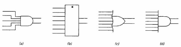
FIG. 11 Accommodation for additional inputs: (a) sometimes used for
a limited number of inputs; (b), (C), and (d) approved by ANSI/IEEE Y32E.
The asterisk is to be replaced by a qualifying symbol or letter, such
as & for AND, 1 for OR.
Sometimes it is desirable to have logic symbols of two or more different sizes on a single diagram. Some of the symbol templates have two sizes of each symbol. One very suitable template is MIL STD 80C.
6 Negative and Mixed Logic
The NAND (NOT AND) function symbol shown in FIG. 9 has a small circle at the junction of the symbol and the output line. This circle is a negative indicator symbol. Its presence provides for the representation of the output in terms independent of its physical value. That is, the 0-state of the output is the 1-state of the symbol. If a circle is placed on the input side of a logic gate, the state or polarity of the input signal is reversed before entering the gate or function.
The result of the negative circle on the output side of an AND gate is that it now performs the NAND function. FIG. 12 shows the effect of having negative logic on all leads of an AND function. The truth table is as follows:
A glance at the truth table for the OR circuit ( FIG. 6) will reveal that these two truth tables are the same. That is, the AND circuit performs the same function in negative logic as the OR circuit performs in positive logic.
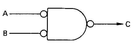
FIG. 12 An AND function having negative indicators at inputs and outputs.
The result of using this negative logic is that the circuit performs
as an OR function.
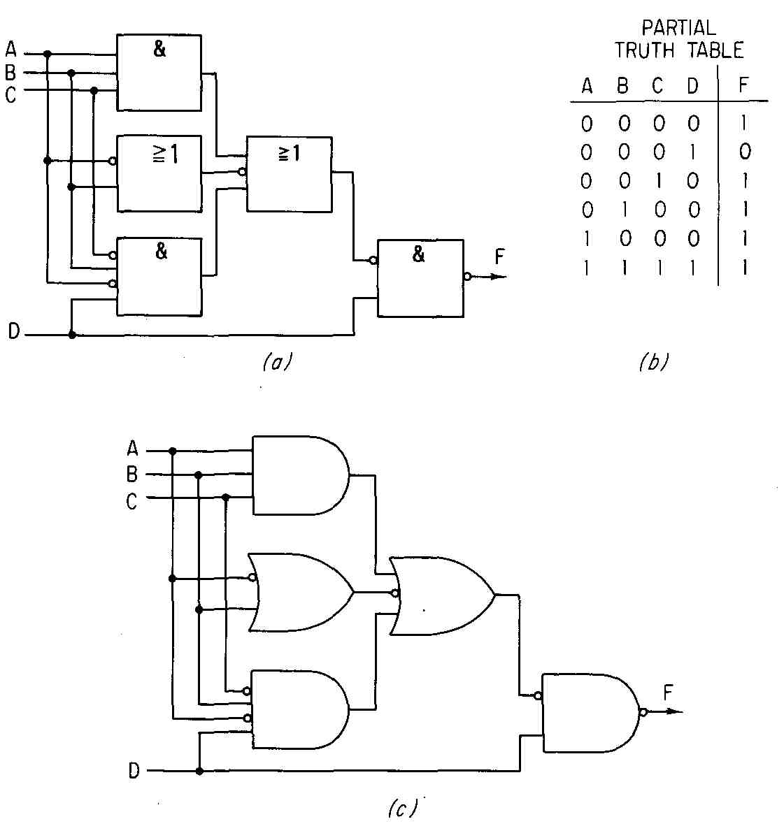
FIG. 13 Example of a logic diagram in which uniform shapes have been
used at a and distinctive shapes at c. The & symbol is for an AND
function, and 1 is for the OR function.
Instead of the letter C for output, some truth tables show the letters AB (the output for the AND function), A + B(the output for the OR function), A (the output for a converter or NOT gate), AB + AB (the output for an Exclusive OR function), AB (the output for a NAND function), and A + B (the output for a NOR, not OR, function). There may be, and often are, more than two inputs into a function, in which case the letters will be changed (see FIG. 13) or omitted entirely.
FIG. 14 has logic symbols that were made by one of the authors on a personal computer. The symbols were developed on the monitor display using basic language. They appear at the right side of the CRT display as a menu. The remainder of the screen is available for drawing a diagram in which these symbols can be used. The figure is the actual printout from a dot matrix printer. The lines are composed of pixels, which are the smallest picture elements that can be made on the tube.
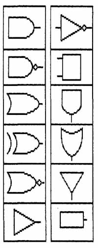
FIG. 14 A menu of logic symbols developed on a PC and printed by a
dot matrix printer.
7 The Decision Table
Somewhat similar to the truth table is the decision table, which is essentially a tabulation of logical relationships consisting of conditions, actions, and rules. Conditions are the variables that influence any decision, while actions are the things to be done once a decision has been made. In the case of BART, San Francisco’s rapid-mass-transit system, Bay Area Rapid Transit ( FIG. 15 and Table 1)1, a computer makes the decision and one of five actions (0 to 4 listed at the bottom of the table) is taken. A CP is a critical point (control location) at which it is especially desirable for trains to be on time.
8 IEC Logic Language and Dependence Notation
The system that is introduced here has been developed by the International Electrotechnical Commission (IEC) to show the relationship between each input of a digital logic circuit to each output without explicitly showing the internal logic. It consists of one or more outlines (mostly rectangles) and one or more qualifying symbols. Some of the qualifying symbols are shown in Tables 2, 6-3, and 4.
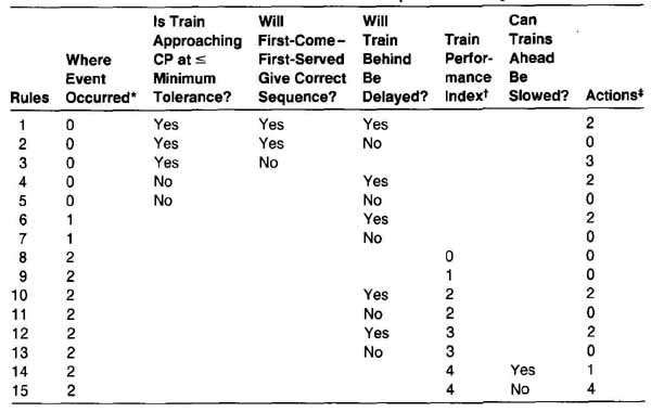
TABLE 1 Decision Table for an Automated Rapid-Transit System
* State 0, between a station and a merge’; state 1, between a station and a CP that is not a merge; state 2, at least one station before a CP.
Action 0, continue with existing schedule; action 1, revise schedules ahead of delayed train to reduce extended gap; action 2, revise schedules behind delayed train to extend reduced gap; action 3, recommend revised sequence at interlocking; action 4, recommend station run-through.
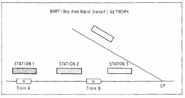
FIG. 15 Simplified drawing of a rapid-transit network illustrates how
the decision table logic matches system conditions with a rule (in this
case rule 14). Rule 14 specifies action 1, which is to reduce the gap
ahead of the delayed train by revising schedules of trains ahead of it.
Input lines are placed on the left and output lines on the right. When an exception to this rule exists, an arrow pointing to the left, upward or downward, is placed along the line. Outlines of elements may be abutted or embedded. If elements are joined by a (common) line that is parallel to the signal flow, there is no connection. If a common line is perpendicular to the signal flow, there is at least one logic connection between the elements.
FIG. 16a shows three digital logic circuits joined together. The AND and OR symbols are shown in each rectangle. In the upper part, the rectangles are joined, as is customary with this system. The lower part of FIG. 16a shows the same arrangement, but as we have previously drawn logic circuits. (See FIG. 13a, where the OR symbols are slightly different.) FIG. 1 6b illustrates another arrangement in which the lower rectangle is a common output element usually separated by two closely spaced parallel lines. In the lower part of FIG. 16b the outputs of the upper two OR functions can be seen going to the lower AND function, using the older system.
TABLE 2 General Qualifying Symbols
TABLE 3 Qualifying Symbols for Inputs and Outputs
TABLE 4 Symbols Inside the Outline
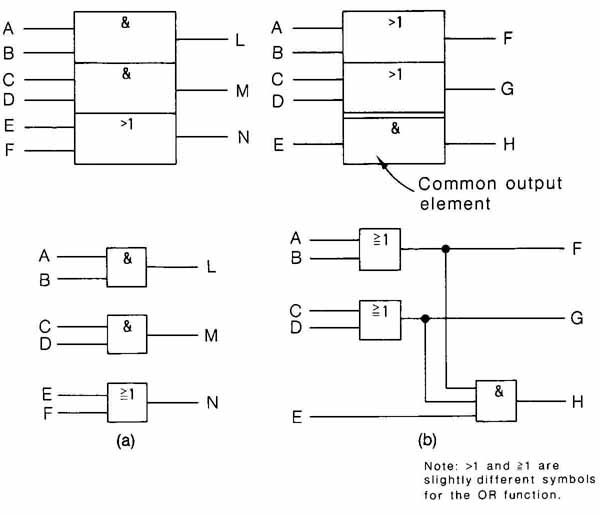
FIG. 16 Symbols used br digital logic circuits in revised IEEE 91 ANSI
Y32.14. Note: >1 and 1 are slightly different symbols for the OR function.
While the two lower diagrams in FIG. 16 may be about as simple to draw as the upper ones, and easier to read and follow, there is a major reason for the development of the IEC symbols. Many digital circuits now contain hundreds and more functions which cannot be drawn in the more traditional diagram form because of space limitations. Also, certain types of circuit, such as shift registers, coders, and latches, require the addition of more information. The example shown in FIG. 17 may help to demonstrate the value of this powerful tool.
FIG. 17a shows the relationship of a common control block symbol. Here we see that the two lower blocks receive the output of the CC block. FIG. 17b makes use of what is called M (mode) dependency. Inputs band c control one of four modes (0 through3) that will exist at any onetime. Inputs d, e, and f are D inputs subject to dynamic control (clocking) by the a input. The numbers I and 2 have been indicated at inputs d, e, and f so that input disenabled only in mode 2 (shifting down and serial loading) and e and f are enabled only in mode 1 (parallel loading). The number 4 (at a, d, e, and f) is an arbitrarily chosen identifying number that labels each input that is affected by the affecting input, which is a in this case. Refer to Table 4.
Input a has three functions. It is the clock for entering data. In mode 2 it causes right-shifting of data, and in mode 3 it causes the contents of a register to be incremented by one. This is what the arrow after the 2 and the plus sign after the 3 signify.
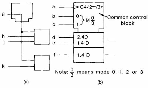
FIG 17 (a) Relationship of a control block to other logic elements.
(b) Logic symbols using M (mode) dependence which affects inputs. Mode
0 (b=0, c=0). Mode 1 (b=1, c0). Mode 2 (b0, c=1). Mode 3 (b=c=1).
Dependence notation is used mostly by persons working with digital design. As can be seen in the situation described above, it can become very complicated. It is beyond the scope of this guide to explain the system in more detail. However the reader should be aware that it exists and that he or she might be exposed to it in the future. More detailed information may be found in IEEE/ANSI Y32.14.
SUMMARY
Flow (or block) diagrams are used for different purposes in different situations. They may be used for depicting an electric circuit or system, for the preliminary design work in computers and other electrical installations, and for programming problems to be solved by computers. A left-to-right direction is sought in planning most block diagrams because this is the normal way in which people read. However, this sequence cannot always be followed. In most block diagrams there is a certain amount of lettering within the blocks. This lettering may determine what the sizes of the blocks will be. Liberal use of arrowheads is made in block-diagram construction. Although the rectangle is widely used in flow and block diagrams, other shapes — and sometimes electrical symbols — are used as dictated by standard practice. Blocks and flow lines should be evenly spaced if a pleasing drawing is desired.
In recent years, the use of distinctive shapes for logic diagrams has become popular. These shapes facilitate the reading of diagrams for complex systems.
QUESTIONS
1. Where are auxiliary circuits, such as feedback, usually placed with regard to the main signal path of a flow diagram?
2. What determines how large the rectangles in a block diagram should be?
Show by means of a freehand sketch.
3. What standard covers the preparation of block or flow diagrams?
4. In making a block diagram of an electrical system, what shapes would you use for the blocks? Why?
5. What direction of flow would you attempt to show in planning a block diagram of an electronic circuit?
6. What are three devices that may be shown by means of standard symbols, rather than by blocks, according to customary practice?
7. What features make the block diagram for a microcomputer distinctive?
8. When might a dashed line be used instead of a solid line in a diagram?
9. Show by means of a freehand sketch how you would lay out a flow diagram with, say, 10 blocks, too many to fit on a single line on an 8 X 11 sheet.
10. Define the word stage.
11. Sketch six different shapes that may be used at one time or another in logic diagrams. Label each shape.
12. What are five different functions that might be shown with the rectangle in logic diagrams?
13. With negative logic (circles) used at all outputs, what does a NAND circuit perform? What does a NOR circuit perform?
14. What is the difference between an Exclusive OR circuit and an OR circuit? (Show by means of truth tables.)
15. Add the missing lines of the partial truth table of FIG. 13b for A and B only, in the 1-state; A and D only, in the 1-state.
16. What are the advantages of using distinctive shapes, rather than uniform shapes, in a logic diagram? What is one disadvantage?
17. What are the similarities between a decision table and a truth table? The differences?
PROBLEMS
1. Make a block (flow) diagram for an AM radio receiver as follows:
a. External antenna
b. RF amplifier
c. Mixer
d. IF amplifier
e. Detector
f. AF amplifier
g. Speaker
h. Oscillator (feeds into mixer)
Show an AGC feedback from the detector to the RF amplifier and IF amplifiers. Make neat uppercase lettering in the blocks using appropriate abbreviations. Use 8+ X 11 paper (tight fit) or 11 X 17 or 12 X 18 paper.
2. Make a simplified block diagram for a digital watch as follows. Use a left-to-right sequence for the first four blocks, as follows: (1) quartz crystal, (2) oscillator, (3) frequency divider, (4) wave shaper, (5) battery (with lines flowing to oscillator, frequency divider, and wave shaper), (6) decoder (with lines flowing from battery and wave shaper), and (7) digital readout (line flowing from decoder). Make neat uppercase lettering in the blocks, using appropriate abbreviations.
3. Make a block diagram for the following (TR 9-10 BC-Sw) radio receiver (follow the instructions given in Prob. 1):
a. External antenna
b. Mixer
c. First IF amplifier
d. Second IF amplifier
e. AF amplifier
f. Driver
g. Output stage
h. Earphone or speaker jack
i. Oscillator to feed into the mixer; and AGC feedback around the IF stages
Use 11 X 17 or 12 X 18 paper unless drawn as two lines, in which case it might fit on 8+ X 11 paper.
4. Make a block diagram for the following FM radio receiver (see instructions given in Prob. 1):
a. Antenna
b. FM RF amplifier
c. FM converter
d. First FM IF amplifier
e. Second FM IF amplifier
f. Third FM IF amplifier
g. AF amplifier
h. Output stage
i. Jack
Use 11 X 17 or 12 X 18 paper.
5. FIG. 18 shows the partially completed flow diagram for the control system for Solar One, the central receiver electric generating plant in California.
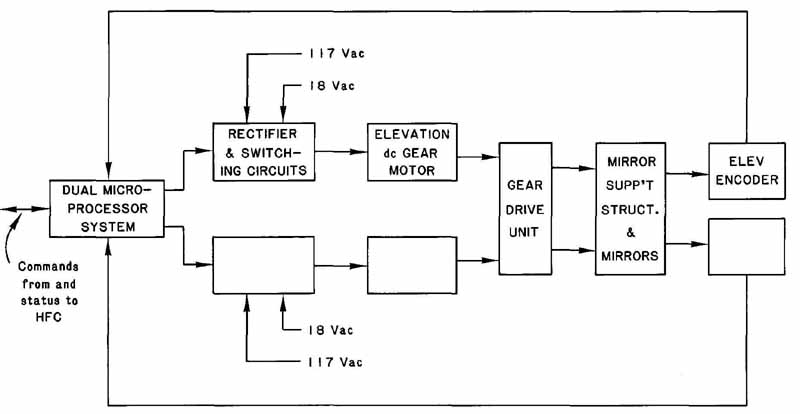
FIG. 18 ( Prob. 5.) Flow diagram for solar central receiver electric
generating plant.
Each heliostat reflector has a gear-motor for changing elevation and another for changing azimuth (the horizontal angle). Draw the complete diagram for this control system, showing rectifier, switching, gear-motor, and encoders for the azimuth movement below the corresponding blocks for elevation. Make neat uppercase lettering in the blocks using appropriate abbreviations. Use 8 - X 11 (tight fit) or 11 X 17 or 12 X 18 paper. (The abbreviation HFC means heliostat field controller.)
6. Complete the drawing of the code converter in FIG. 19 by showing distinctive shapes for the NAND and Exclusive OR gates. Draw a border around the entire diagram, including the number 8. Dots are optional. Use 8 11 paper.
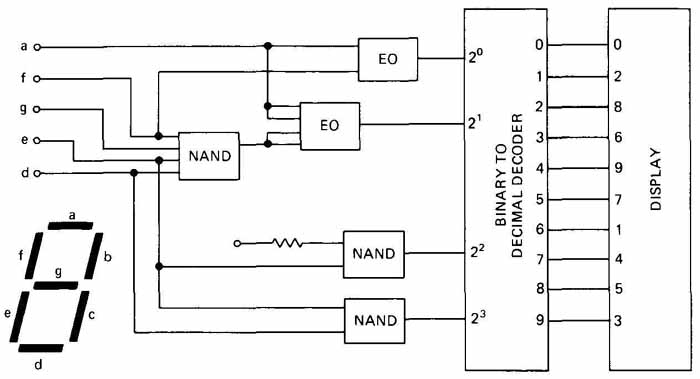
FIG. 19 ( Prob. 6.) Code converter circuit.
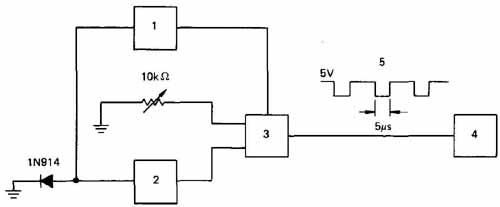
FIG. 20 ( Prob. 8.) Automobile temperature-measuring circuit.
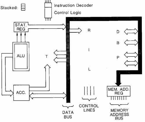
FIG. 21 ( Prob. 9.) Incomplete flow diagram of a microprocessor.
7. Construct a block diagram for a basic regulating system that has the following steps or devices:
a. Power source
b. Regulated quantity
c. Signal-sensing device
d. Error-sensing device
e. Reference
f. Amplifier with feedback
g. Regulator power source
Such a regulating system could be used for the speed control of a motor. In such a case, the motor would be the regulated quantity and a tachometer would be the signal-sensing device. Use 8 X 11 paper.
8. Make a block diagram of the automobile temperature-measuring and readout circuit shown in FIG. 20. Block 1 is the forward-feed compensator, 2 is the capacitor reset, 3 is the operational amplifier, and 4 is the TTL converter. Above the waveform at 5, label “1-Hz square wave.” The diode is a tempera ture-sensing diode. Do not show digits 1 through 5.
9. FIG. 21 shows the incomplete flow diagram of a microprocessor. Redraw the diagram, and add the following elements where their location is indicated by capital letters:
T — storage registers, two stacked; show connected to the ALU with output arrows and to the accumulator and data bus with input arrows
R — instruction register below which and connected to it is I, the instruction decoder, below which and touching it is L, the control logic (see sketch at top)
D — D register
B — B register
P — Program counters, two stacked
Put the letters or appropriate abbreviation for each element in its block. Label the bus: “Internal data bus.” This will fit on a 8.5 X 11 sheet.
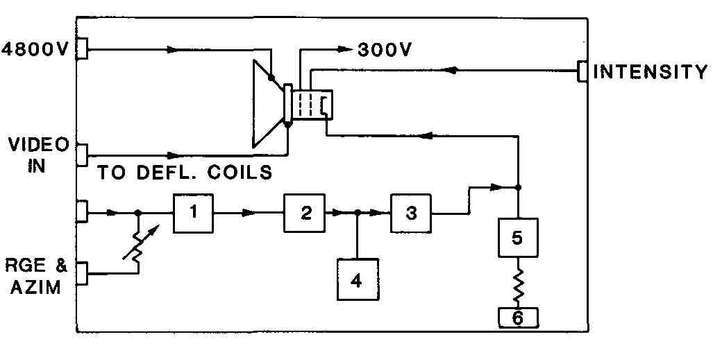
FIG. 22 ( Prob. 10.) Indicator block diagram for airborne radar.
10. Complete the flow diagram displayed in FIG. 22 by placing the following titles in the boxes indicated by the numbers: 1, video mixer; 2, video amplifier; 3, video amplifier; 4, DC restorer; and 5, DC restorer. At 6 replace the block with a ground symbol.
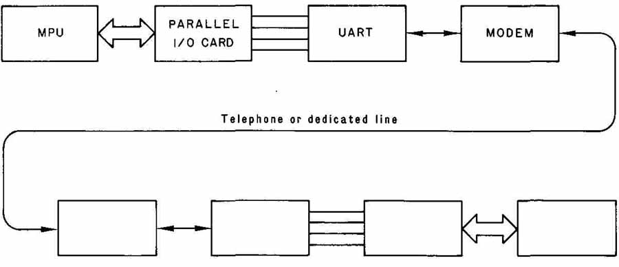
FIG 23 ( Prob. 11.) Diagram showing use of modems for communicating
over long distances. Modems (modulator-demodulators) send and receive
digital signals by using different tone signals for logic “1”s and “0”s.
11. Refer to FIG. 23. The diagram shown is for a system that communicates digital signals over long distances. The UART is a universal asynchronous receiver-transmitter that converts parallel data to serial data which can be transmitted by the modem and vice versa. Draw the flow diagram as it is shown and complete the diagram by lettering the names or abbreviations of the elements in the lower blocks. These are the reverse of the ones above; i.e., the modem is at the left and the microprocessor (MPU) is at the right. Use 8.5 X 11 paper.
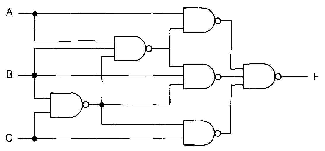
FIG. 24 ( Prob. 12.) A NAND network in a gate array. (Texas Instruments, Inc.)
12. Refer to FIG. 24. The NAND gate is part of a gate-array package. Redraw this gate, using distinctive shape or rectangular symbols with appropriate abbreviations. On the same 8.5 X 11 sheet construct a truth table if so requested by your instructor.
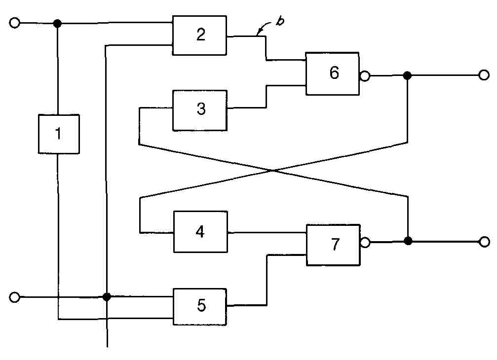
FIG. 25 ( Prob. 13.) A data storage latch. (Texas Instruments, Inc.)
13. Refer to FIG. 25. This logic diagram of a storage latch contains an inverter at 1; AND functions at 2, 3, 4, and 5; and NOR functions at 6 and 7. Draw the logic diagram, using rectangular shapes with suitable notation or distinctive shape symbols, whichever your instructor indicates. The diagram would look neater if symbol 6 were raised so that line b would be a single straight line. Use 8 X 11 paper.
FIG. 26 ( Prob. 14.) A J-K flip-flop circuit.
14. Refer to FIG. 26. The diagram of the J-K flip-flop circuit consists of rectangular symbols. Redraw this circuit on 8.5 X 11 paper, using distinctive shapes for the logic functions.
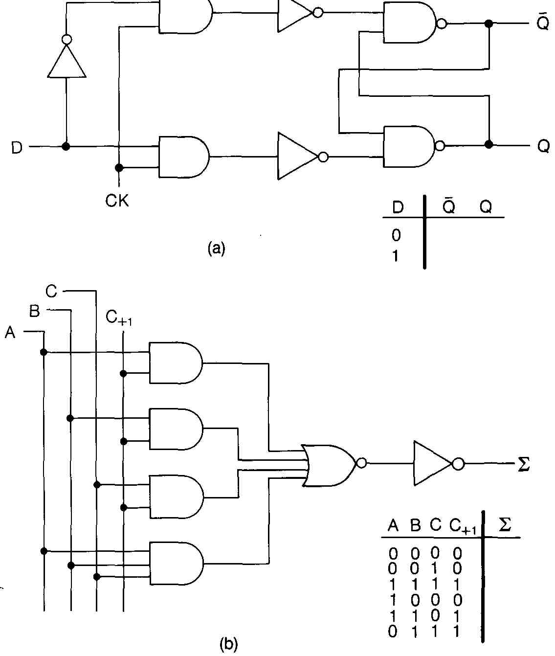
FIG. 27 ( Prob. 15.) Logic diagrams for (a) a flip flop and (b) an adder circuit.
15. Refer to FIG. 27. Complete the truth tables for the flip-flop and adder circuits shown. Assume that the clock (CK) circuit is “on” in part a. Show the output at I for the six cases of inputs listed for A, B, C, and C in part b. Display your results neatly on whatever paper your instructor desires. Draw the logic diagrams if your instructor requests you to do so.