AMAZON multi-meters discounts AMAZON oscilloscope discounts
The schematic diagram is often the primary drawing of the electronics and communications industry. It is a diagram that shows the functions and relationships of a circuit by means of graphical symbols. It does not show the physical layout of those components, however.
The schematic diagram usually includes electronic and certain passive components. A similar type diagram, involving electromechanical devices, is called the elementary diagram. It is discussed in Sections 9 and 10.
The schematic diagram makes it possible for a person with an electronics background to trace and understand a circuit with comparative ease. For this reason it is used for design and analysis of circuits, instructional purposes, and maintenance troubleshooting of circuits.
1. Examples of Transistors in Circuit Drawings
In order to give the student a “feel” for the layout of schematic diagrams, we shall present several figures showing popular formats now in use. Then the problem of laying out such a diagram will be discussed. (Without much back ground in electronics it may not be possible to understand all the authors’ comments about the following circuits, but it should be possible to visualize the different drawing patterns that are shown.)
FIG. 1 shows the three methods of connecting a bipolar transistor in a circuit: common base (or grounded base), common collector, and common emitter. In the common-base circuit ( FIG. la), for example, the signal (shown by the in the circle, which indicates an ac input) is introduced into the emitter-base circuit and extracted from the collector-base circuit. The base is thus common to both the input and output circuits. The direction of the arrows shows the electron flow. The voltage or power gain may be in the order of 1500, and the phase of the signal is not changed.
In the common-collector arrangement ( FIG. 1b) the signal is introduced into the base-collector circuit and extracted from the emitter-collector circuit. The power gain is lower than in the other two configurations, and there is no phase reversal. This arrangement is used primarily as an impedance-matching device.
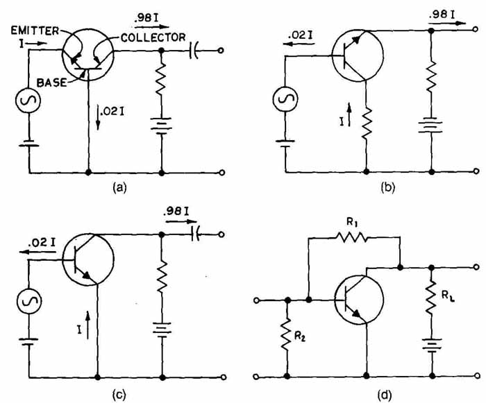
FIG. 1 Basic bipolar transistor circuits: (a) common base; (b) common
collector; (C) common emitter; (d) bias network for common emitter circuit.
The common-emitter circuit ( FIG. 1c) can provide power gains of 10,000. The input signal is introduced to the base-emitter circuit, and the output is taken from the collector-emitter circuit. However, this arrangement is the most widely used when more than one stage is required.
FIG. 1d shows a popular biasing arrangement for a common-emitter circuit, which does away with one of the batteries used previously. (Bias is the difference in potential between, say, the collector and the base.) A voltage-divider network composed of R and R provides the required forward bias across the base-emitter junction.
In the examples shown, NPN transistors have been used; PNP transistors could be used instead, in which case the battery polarities and the direction of the arrow on the emitter should be reversed.
2. The Basic Amplifier
Three major functions of transistors and electron tubes are amplification, oscillation, and switching.
FIG. 2a shows a common emitter amplifier circuit using a PNP transistor. Such amplifiers are used in audio circuits. The input is applied across R , and the output is taken between collector and ground. FIG. 2b shows a similar amplifier using a triode electron vacuum tube. Again, the input is applied across R and the output is taken between the plate and ground.
* In the figure, R is shown as RI. In many schematic drawings the letter and number are the same height.
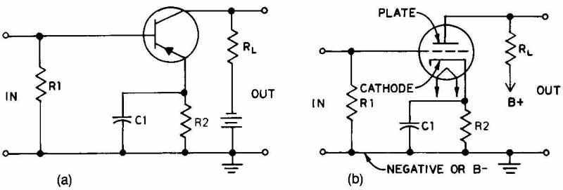
FIG. 2 Basic amplifier circuits: (a) transistor; (b) vacuum tube.
3. Interstage Coupling
In the main, there are three methods by which two or more stages (amplifier stages, for example) may be hooked together. These three methods are: (1) RC (resistance-capacitance), (2) transformer, and (3) DC (direct coupling). Each has its advantages and disadvantages. FIG. 3 shows examples of these methods.
FIG. 3a shows part of a resistance-capacitance-coupled amplifier. Capacitor C is called the coupling capacitor. This method is widely used because of its low cost and the large range of frequencies that can be handled.
FIG. 3b shows a transformer-coupled network in which one side can be “tuned.” (Note that in FIG. 3b and c the transistor symbols have not been enclosed by an envelope circle. The reader may recall that the circle is optional. The authors have omitted the circle from these two circuit drawings on purpose to remind the reader that it is not always used. The authors prefer the circle, however, and use it in most examples in the guide.) Transformer coupling may also be employed in which both sides or neither side is tuned. Tuning makes possible frequency selection.
FIG. 3c shows a direct-coupled circuit, which regulates the circuit so that the output voltage is maintained nearly constant. Typical applications include output stages of series-type and shunt-type regulating circuits, chopper circuits, and differential and pulse amplifiers. Obviously, the cost is low for this type of coupling, and it is, therefore, widely used.
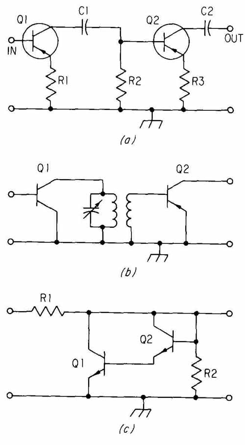
FIG. 3 Methods of coupling amplifier stages together: (a) RC coupling;
(b) transformer coupling; (C) direct coupling.
4. Patterns for Transistor Circuits
The nature of the circuitry, including coupling circuits, often indicates a pattern to the engineer or drafter who is making the final sketch or layout drawing of an electronics circuit. The drawing should be planned to allow the pattern to develop in as auspicious a manner as possible.
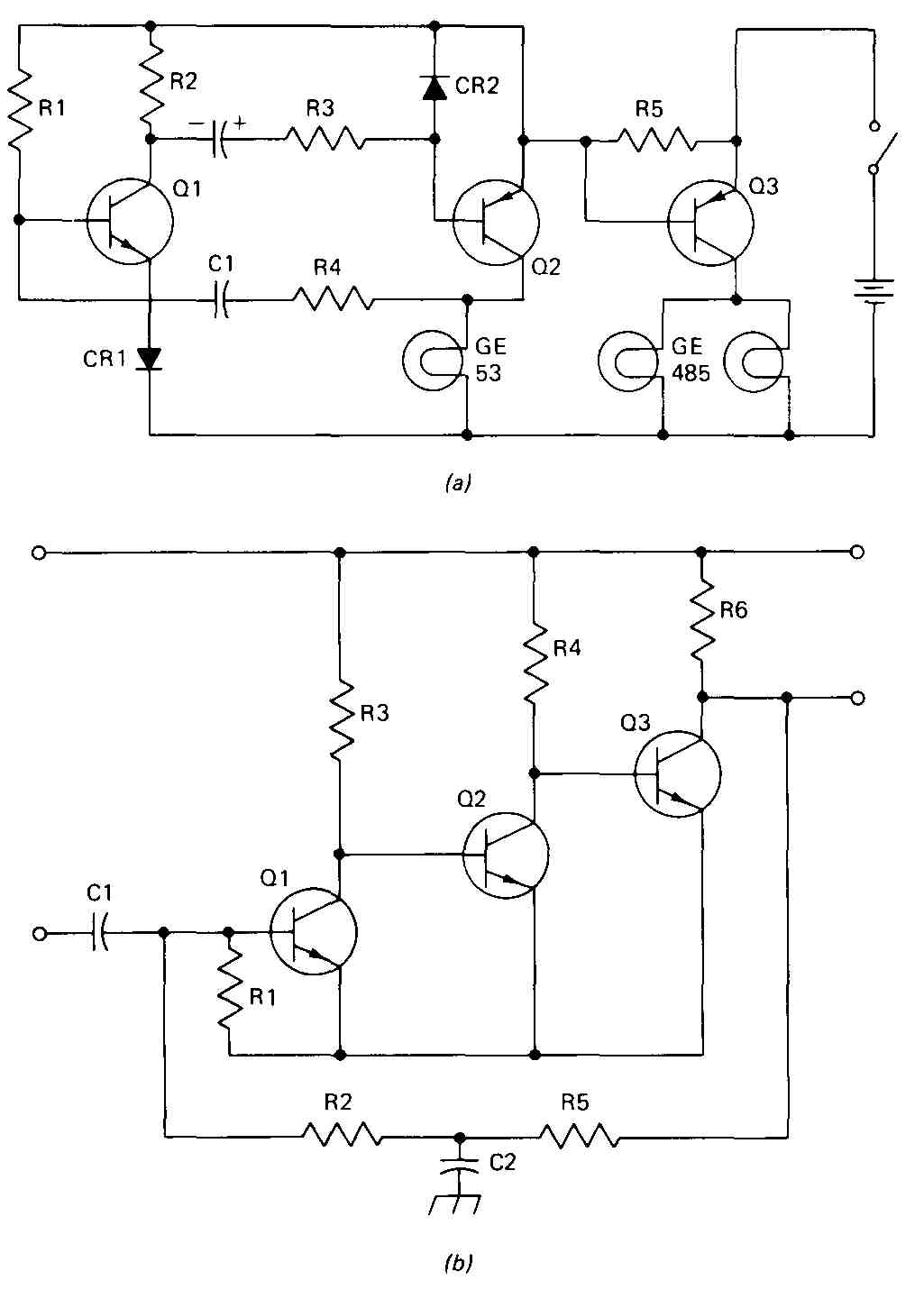
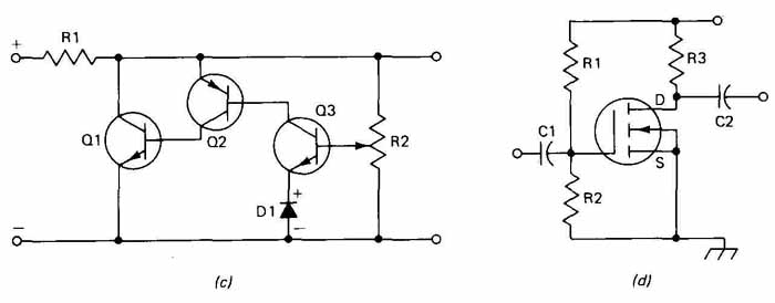
FIG. 4 Different arrangement patterns of transistors in circuits: (a)
horizontal alignment as in this flasher circuit; (b) incline as in this
DC amplifier circuit; (C) staggered as in this shunt regulator circuit;
(d) circuit with MOSFET transistor.
FIG. 4a shows a flasher circuit for emergency vehicles, barricades, boats, and aircraft. It will be noted how the transistors are aligned on a horizontal line (invisible), as are the flasher lamps and some other components of the circuit. This horizontal transistor alignment is possible in many circuits, including radio and television.
FIG. 4b shows an incline pattern which develops because of the direct coupling of the transistors. The second and third stages are biased by the preceding stages.
FIG. 4c shows a staggered pattern which develops when, for instance, PNP and NPN transistors are used in a DC arrangement.
A vertical arrangement of transistors is shown in FIG. In a push-pull circuit, such as that shown in FIG. 5a, each transistor amplifies half the signal, and these half-signals are then combined in the output (collector) circuit to restore the original waveform in an amplified state. This circuit requires trans former coupling, while that of FIG. Sb does not. In this circuit, showing electron current flow by means of arrows, essentially no dc flows through resistor RL. Therefore the voice coil of a speaker can be connected in place of RL without excessive speaker-cone distortion.
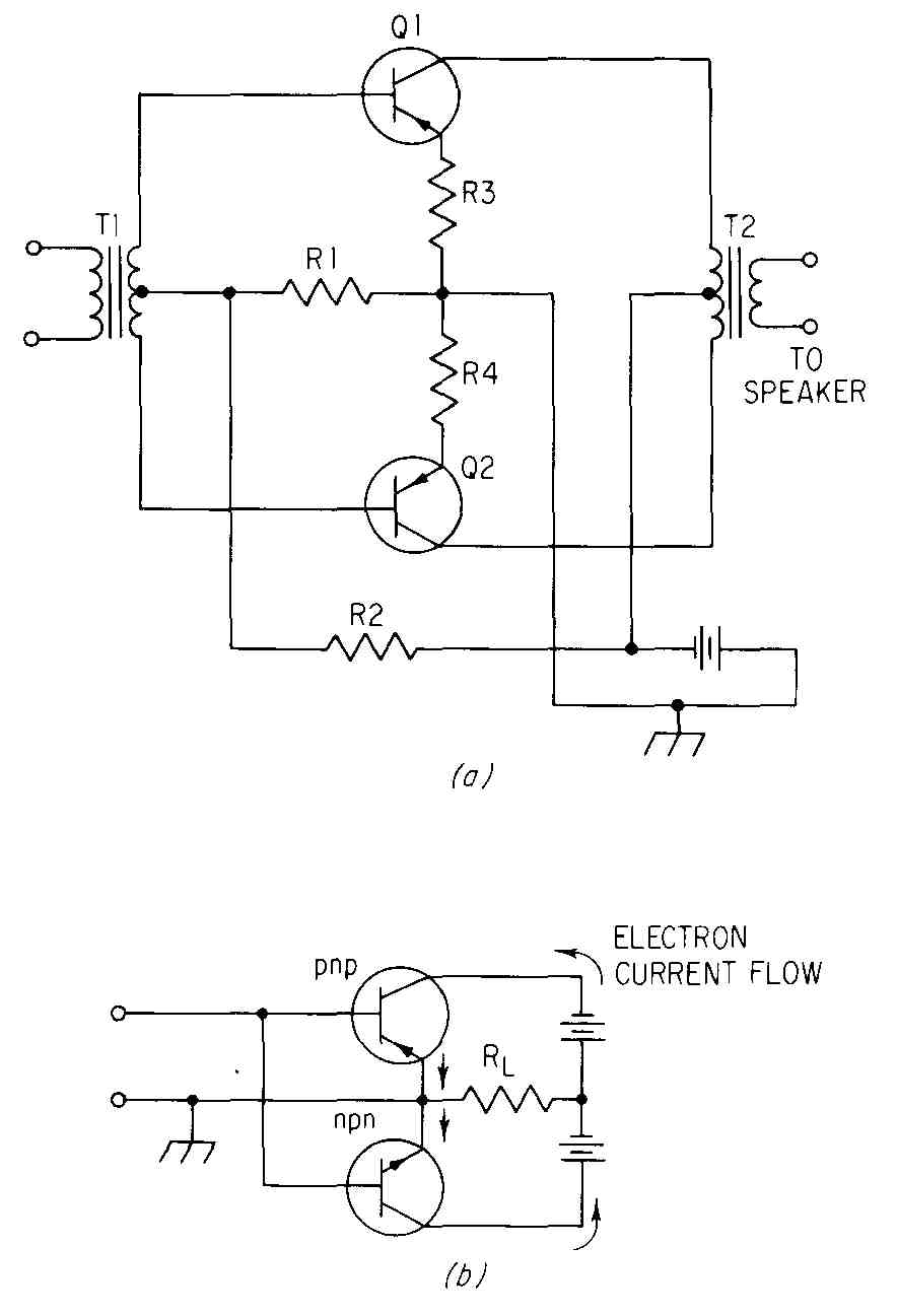
FIG. 5 Vertical alignment pattern of transistors: (a) a push-pull amplifier;
(b) basic complimentary-symmetry circuit.
5. Examples of Computer Circuits
FIG. 6a shows a saturated flip-flop circuit having one input, called a trigger, at T and outputs at A and B. A flip-flop is a memory, or storage, device that may have one of two states, ON or OFF. It always has two complementary level outputs and may have one, two, or three inputs.
A common feature of flip-flop circuit drawings is the crossing, angled, signal-path lines near the center of the circuit. Inmost other electrical drawings, the signal paths are drawn as horizontal or vertical lines. It would be possible to draw a flip-flop in this manner, too, but most companies now use the angled lines.
Another type of flip-flop is the set-reset, which is shown by means of a block diagram in FIG. 6c. In this circuit, a pulse at S (set) input causes the flip-flop to turn on or stay on, depending on the original state. An input at R (reset) causes the circuit to turn off or stay off.
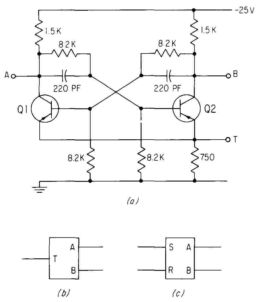
FIG. 6 Horizontal alignment of transistor in flip-flop circuits: (a)
schematic diagram of T type; (b) block diagram of T type; (C) RS type.
FIG. 7 shows several typical logic circuits that are manufactured as integrated circuits (ICs). There is only one type of logic, namely Boolean. However, today it is common to hear the component configuration referred to as a type of logic, i.e., transistor-transistor logic (TTL), CMOS logic, etc. These circuits are found in IC manufacturers’ catalogs; however, because of the steadily increasing circuit complexity, there is a trend to show only the logic symbols for ICs.
6. Reference Designations
Symbols of all replaceable parts should be referenced. A reference may be placed above, below, or on either side of its part. Practice recommended by ANSI includes giving each part a number, such as resistor R and its capacity, such as 100 ohm. Thus we have two lines of designations (combinations of letters and numbers) for most elements in a circuit. Table 1 gives letters and examples that are typical of standard practice. Figures 10 and 15 are good examples.
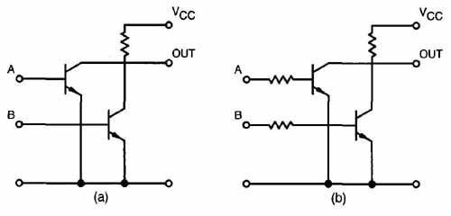
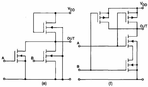
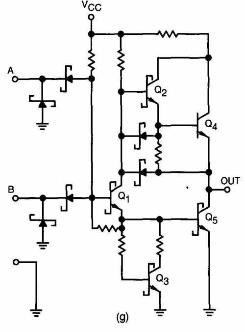
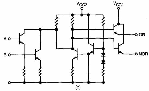
FIG. 7 Digital ICs: (a) direct-coupled transistor logic (DCTL) (archaic)
two-input NOR gate; (b) resistor-to-transistor logic (RTC) (archaic)
two-input NOR gate; (C) resistor-capacitor-transistor logic (RCTC) (archaic)
two-input NOR gate; (d) transistor-to-transistor logic (TTL) two-input
NAND gate; (e) negative channel metal- oxide semiconductor (NMOS) two-input
NOR gate; (f) complimentary metal-oxide semiconductor (CMOS) two-input
NAND gate; (g) Schottky TTL (STTL) two-input NAND gate; (h) electron-coupled
logic (ECL) two-input NOR/OR gate with vertical bias network.
The abbreviation mH (often MH in drawings) stands for milli-henry, a thousandth of a henry. The abbreviation pF (often PF or UUF in drawings) stands for picofarad or micro-micro-farad (a millionth of a millionth of a farad).
The letter X is sometimes used for transistors, although Q is recommended by both the Military and American National Standards. The symbol R does not mean the 201st resistor in the circuit. It means that it is the first resistor in the second (200 series) subassembly. Both the transistor and the tube contain a third line — their function. This is optional information insofar as the drawing is concerned.*
* In a schematic drawing each line of letters or numbers is centered, that is, 270 is centered under R201 and 2N482 and DETECTOR are centered under Q5.
7 Laying Out a Schematic Diagram
FIG. 8 shows a freehand sketch of a light-flasher circuit. This is the type of sketch that might be made by a design engineer or project chief. The purpose of the sketch is to furnish all the information necessary to make a finished drawing of this circuit and to construct it. If the sketch is very rough and there are many places where improvement is indicated, it may be desirable to make a new sketch.
A drafter should produce a well-balanced work that is pleasing to the eye. In order to do this, it may be necessary to change the configuration of the drawing (reorient some symbols and change some lines), but the circuit must still maintain its original technical significance. One must also strive for simplicity and clarity.
A glance at FIG. 8 reveals that, among other things, the transistors could be lined up better, it is a little crowded in the shaded region, and the sketcher has used loops for crossovers— a nonstandard procedure. Also, the components do not have reference numbers.
FIG. 8 Freehand sketch of a light-flasher circuit.
FIG. 9 shows how one can go about correcting some of these deficiencies and starting the layout of the diagram. FIG. 9a shows how the spacing between vertical lines in the crowded area can be determined by lettering the appropriate reference designations, possibly on a trial basis on a sheet of scratch paper, or on the new sketch if such is being made.
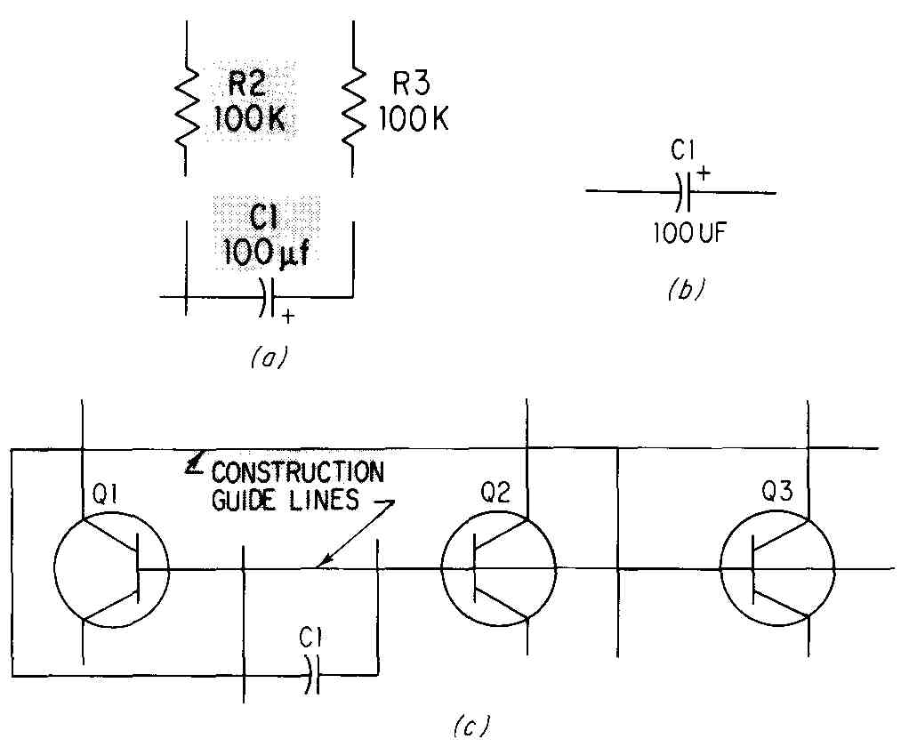
FIG. 9 Details in laying out a schematic diagram: (a) allowing space
for reference designations (identification); (b) alternative arrangement
for referencing capacitor; (C) using horizontal guidelines for transistors
and other line work.
It is obvious that three, and probably all four, transistors can be aligned on one horizontal line to make for a more pleasing and professional-appearing drawing. Therefore, a light construction centerline can be drawn horizontally at about mid-height through the drawing area. At this time, or possibly later, after more components have been drawn, other horizontal guidelines can be drawn in. One other such line is shown in FIG. 9c for the collector outputs.
The transistor envelope circles can be drawn in at this time if the spacing between them can conveniently be determined. FIG. 9a has provided the spacing around C , and, by allowing a little more spacing on each side of the vertical lines (on which R and R are located), we can locate Q and Q without much fear of having to redraw the diagram. Because there are no components between the other transistors, we can locate them at this time without much difficulty. [that this is DC (direct-coupled) circuitry. If it were transformer-coupled, much more work and planning would be necessary.]
After putting in the bases, collectors, and emitters, one can draw more lines, such as appear in FIG. 9c, and be well on the way toward completing the circuit diagram. One logical step to perform next would be to draw resistor R or R (reoriented from the sketch).’ Then all five resistors could be located at the same level, and the uppermost horizontal line could be located.
FIG. 10 shows the finished schematic diagram of the flasher circuit (ANSI referencing has been used). Transistor identification has been placed close to each envelope with larger-than-average letters. The authors have used this arrangement (putting the designations above and in line with the individual transistors) rather than putting the designations at the top of the diagram, which is also approved practice. Note that the entire drawing appears to be symmetrical and that a fairly uniform density is apparent. There are often notes of a general or specific nature at the bottom of an elementary diagram, and this one is no exception. Instead of locating transistor Q as shown, we might have drawn a horizontal line from the output of Q to Q and thus would have placed Q “above” the other transistors.
Another popular way to lay out a schematic diagram is to use standard grids. A preliminary sketch can be made on sketching paper having grids, or a grid sheet can be placed under the tracing paper or film on which the drawing is to be made. FIG. 11 shows a layout of the flip-flop circuit on a i-in. (6.4- mm) grid. The grid lines have been used not only as guides for the circuit paths but also as guidelines for making the resistor symbols. The -i-in. (6.4-mm) resistors and 1-in. (25.4-mm) transistor envelopes were larger than those that are drawn on most diagrams before they were reduced for printing.
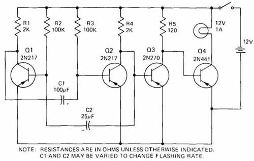
FIG. 10 The completed schematic diagram of a flasher circuit. (From
a circuit in the RCA Transistor Manual.)
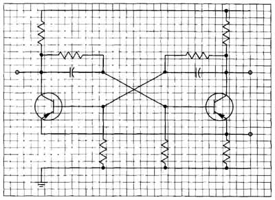
FIG. 11 Layout of a flip-flop circuit on a -in. (6.4-mm) grid.
FIG. 12 shows a null-detector circuit made on a k-in. (2.54-mm) grid with heavy lines 1 in. (25.4 mm) apart. All signal paths have been drawn right
* We will use numbers and capital letters of the same height in the final schematic drawing.
NOTE: RESISTANCES ARE IN OHMS UNLESS OTHERWISE INDICATED. C1 AND C2 MAY BE VARIED TO CHANGE FLASHING RATE.
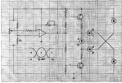
FIG. 12 Layout of a null detector circuit on a i-in. (2.54-mm) grid.
The reader will have to look ahead to FIG. 10 to see which resistors have been assigned designations R and R over grid lines, most on the heavy lines. Small grid lines have been used as guidelines for the resistors and to establish the LED envelopes at 0.6-in. (15- mm) diameter. A graph has been added to show that if a resistor is matched against a reference, a diode A will light up when the resistor R is exactly or closely matched. If the resistor is less than the reference, diode B comes on, etc. The two transistor envelopes are 0.75 in. (19 mm) in diameter, exactly the size shown in ANSI/IEEE Y32E 1976.1 Although most signal paths are drawn horizontally or vertically, in Figs. 11 and 12 there are lines drawn at other angles. These are two types of circuit, along with multi-vibrators and bridges, in which it is customary to show certain lines in this manner. Inmost drawings the paths are horizontal or vertical.
Drawings for manuals and journals are made in ink and often are produced using Leroy equipment. Working from a rough sketch, the drafter lays out a neat pencil drawing with or without a grid, as above. The final drawing is made on Mylar or similar film, which is placed over the pencil drawing. Then the symbols are made with the template and scriber as shown in FIG. 13a. The next step is to draw the signal paths between the symbols with a technical fountain pen such as the Rapidograph or Staedtler-Mars “700,” as in FIG. 13b. Lettering is then put on the drawing. This is done with a Leroy lettering template and scriber, or it is accomplished by using an IBM typewriter and cutting out small rectangles of typed lettering which can be pasted on the drawing at the desired locations. Leroy electrical templates are available with three sizes of symbols and thus provide the layout person with considerable flexibility. Both Leroy lettering templates and typed-lettering “stick-ons” also have much flexibility in the size of letters. Typed letters provide a little more uniformity and a cleaner appearance and save a little time if there is consider able lettering on a drawing.
1. This is somewhat larger than in the previous edition of the standard.
2. Leroy is a registered trademark of the Keuffel & Esser Company.
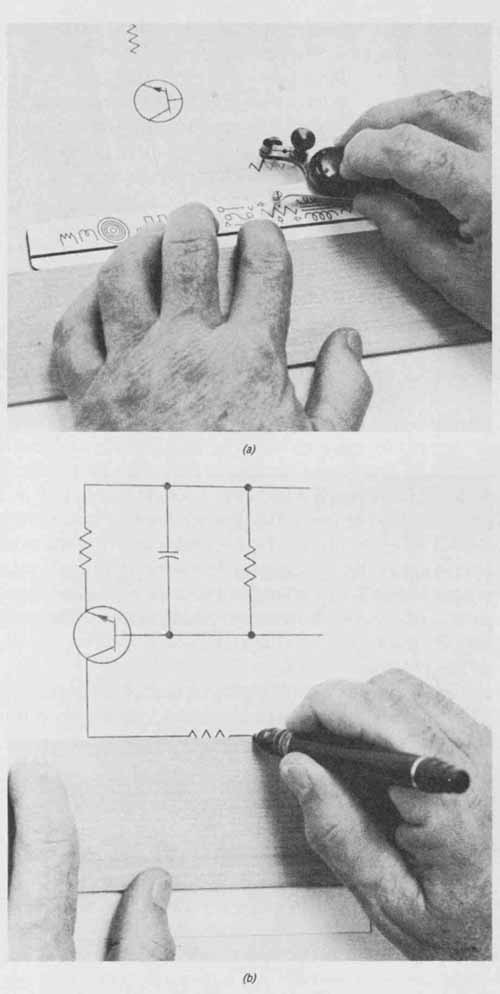
FIG. 13 The use of mechanical devices (scribes and pens) to lay out
a schematic diagram: (a) using a Leroy scriber and template to make symbols;
(b) using a technical pen to draw signal paths between symbols.
Still another approach is to use preprinted device symbols in the form of appliqués or stick-ons. Signal paths are made with pressure-sensitive tapes, pencil, or technical fountain pen. As in the method described immediately above, the detailer probably works from a rough sketch. A neat pencil layout of the diagram is then made either on a grid or on plain tracing paper. Symbols may be sketched in, omitted, or partially drawn on this layout if the final layout will be made on another sheet (overlay), which will be placed over the pencil layout.
In the location indicated on the overlay sheet, each pressure-sensitive symbol is oriented in the precise position by permanently and firmly affixing it to the surface of the artwork. A smaller symbol can be separated from the backing material by inserting a knife (with an X-acto No. 11 or No. 16 blade) in between. The symbol is carried to the desired diagram location on the knife, which is also used as a holding and positioning tool. After the symbols are in place, signal paths are put on the diagram. If inked lines are to be used, they can be drawn as shown in FIG. 13b with a technical or a ruling pen. Pencil lines will not look as good as ink lines because the printed stick-on symbols will be darker. Lettering is usually put on the drawing at the last. FIG. 14c shows a sample sheet of pressure-sensitive symbols.
Many students will not have access to appliqués and Leroy equipment. They will probably have to make all lines and symbols with a pencil. The following fundamentals of layout should be observed:
1. Use medium-weight lines for all symbols and signal paths. When emphasis on a component is desired, use a heavier line.
2. Arrange the diagram so that it reads functionally from left to right, if possible.
3. Strive for uniform density so that there are no congested areas and a minimum of large white areas.
4. Draw signal paths vertically or horizontally, except in special cases such as flip-flop circuits.
5. Keep turns or bends to a minimum. Route all connecting lines as directly as possible.
6. Keep the device symbols in proportion to each other. Use only one size of symbol for each device, if possible.
7. Allow adequate space near each symbol for proper identification.
8. Make integrated-circuit and microprocessor outlines large enough for pertinent lettering to be placed within the outline.
9. Center each symbol along its lead line (signal path).
10. Place the complete identification (and values if necessary) beside or within each symbol, whichever is appropriate. Identify each input and output.
11. Check the final diagram for the correctness of symbols, electrical accuracy, and the presence or absence of connecting dots.
Some aids that are not very expensive might facilitate the drawing of schematic diagrams for students. Grid paper, with or without drop-outlines, is one such aid. A template that makes different sizes of circles or that includes electronic device symbols is another aid. The use of templates is discussed in Section 1.
8. Line Arrangements According to Voltages
Although the circuit shown in Figs. 8 to 10 does not become involved in this problem, some circuit diagrams will have lines representing several different voltages. A good practice is to draw the schematic diagrams so that the highest voltage is on the uppermost line, the next highest is on the line below, and, finally, the most negative voltage is on the lowest line. This makes for easier reading of the elementary diagram in many cases. Typical voltage sequences might be as follows:
235 V
150 V
6.3 V
0 V
—45 V
The top line is what is known as the B+ line; the zero line is the B—, or common, line and may be joined to the ground or chassis. Transistor circuits, as a rule, do not have as many lines as this, but tube circuits may have this many, depending on the circuit and types of tube.
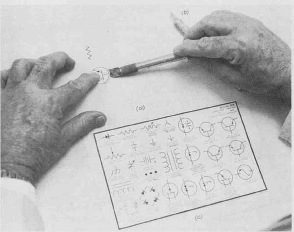
FIG. 14 The use of appliqués for construction of schematics: (a) applying
a symbol; (b) a knife with X-acto No. 16 blade; (C) typical symbols that
are available as pressure-sensitive adhesives. (Bishop Graphics, Inc.)
9. Examples of Schematic Diagrams
FIG. 15 shows the complete schematic diagram of a transistor radio. This particular circuit has a separate mixer and oscillator, two IF stages, a detector and audio amplifier, and a class B push-pull output. The transformer coils are drawn as a series of complete loops. This loop, or helix, is one of two symbols that are approved in the standard. Most drawings now have the simpler symbol, as shown in the power-supply transformer ( FIG. 16). The authors prefer the simpler transformer symbol because it does not clutter up the drawing as much as the old symbol did and is easier to draw. In FIG. 15, L has a metallic core and L has an air core. The authors would be tempted to call L1 and L2 (transformers) T1 and T2.
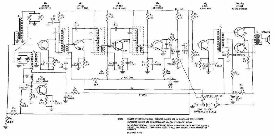
FIG. 15 Schematic diagram of a transistor radio receiver. (From Milton
S. Kiver, Transistors, 3d ed., McGraw-Hill Guide Company, New York, 1962.)
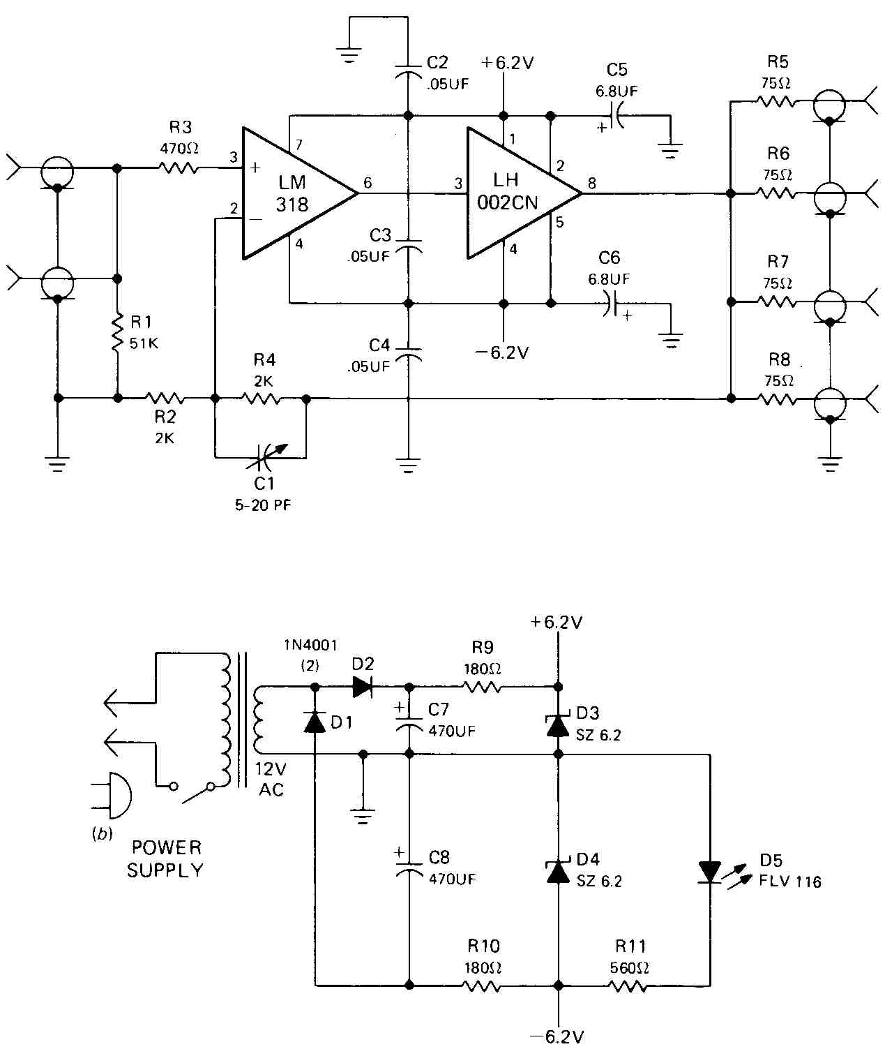
FIG. 16 Schematic diagram of video distribution amplifier and its associated
power supply. (From Electronics magazine, October 13, 1977, p. 121; Copyright
© 1977 by McGraw-Hill, Inc.)
FIG. 16 shows the schematic diagram of a video distribution amplifier that takes the output of a video (TV) camera and provides four independent outputs. The two integrated circuits are an operational amplifier and a current driver in a feedback loop. Inputs and outputs are for coaxial cables. The power supply is placed below the distribution amplifier circuit. This is common practice, although the power circuit could be drawn jointly with the other by joining the 6.8-V lines and (probably) rearranging the whole drawing somewhat. Diodes D3 and D4 are zener diodes used for regulating. A nonstandard symbol in the original drawing, shown at b, was replaced by the standard connectors at the left of the power supply.
FIG. 17 shows the schematic diagrams of two versions of scientific calculators. The calculators are manufactured by the same manufacturer, and the new version ( FIG. 17b) is a replacement for the old version ( FIG. 17a).
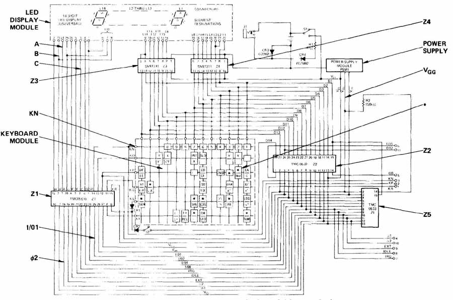
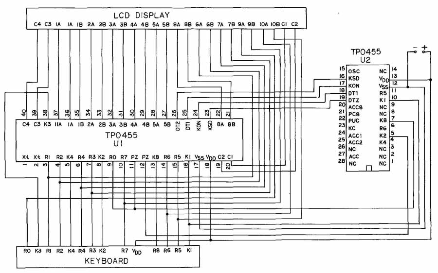
FIG. 17b Schematic diagram of 45 key scientific calculator (newer version).
(Texas Instruments, Inc.)
There are some very interesting differences in comparing the two versions and their associated schematics. For example, the old version has six ICs, while the new version has combined many functions and requires only two ICs. The old version has a schematic of the keyboard and a partially functioned LED display module, while the new version has a schematic symbol for both the keyboard and the LCD display module. Please note that the ICs in FIG. 17a contain an identifier beginning with Z, while the ones in FIG. 17b have an identifier beginning with U. The authors have seen several other identifiers used.
These two calculator schematics have many components and circuits identified; please compare these schematics. Overall, the schematic diagram of the new version is simpler and less cluttered than the old version.