AMAZON multi-meters discounts AMAZON oscilloscope discounts
10. Tube Circuits
FIG. 18 is the schematic diagram of an audio-amplifier circuit having electron tubes. This older drawing has several features worth mentioning. The tubes, except the rectifier 5Y3-GT, have heaters. The heater circuit XX is not drawn in order to simplify the schematic. Loops (no connections) and dots are used. Finally, the values for each component are placed below the diagram. Such an arrangement may make for slower reading of the diagram but has the advantage of supplying more information about each part than can be conveniently shown with the other system. It should be stated that tubes are making a comeback in some audio applications.
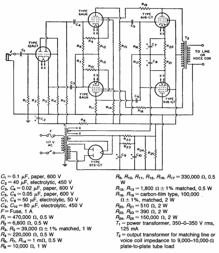
FIG. 18 Schematic diagram of a high-fidelity audio amplifier. (From
RCA Receiving Tube Manual.)
11. Commonly Used Units for Components
In addition to units such as henrys and ohms, certain prefixes (multipliers) are used when components have extremely large or small values. The most often used prefixes are shown in Table 2. Suggested units with their prefixes appear in Table 3.
Some lettering can be saved by using notes such as the one shown in FIG. 10 about resistance values. A similar note might be: Al/capacitance values are in microfarads unless otherwise shown.
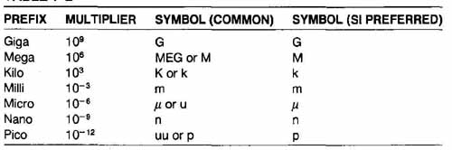
TABLE 2
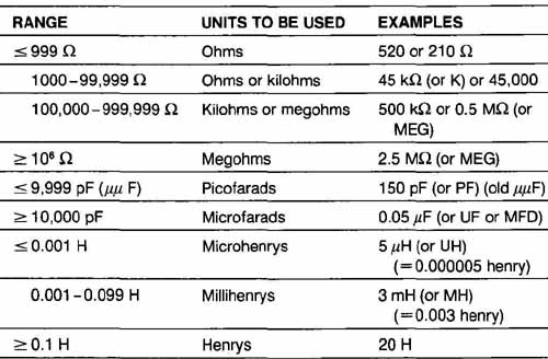
TABLE 3
Tables 2 and 3 present what the authors believe to be current practice relative to prefix values for units. We believe this will continue for years to come. However, it should be pointed out that two new standards may bring about some changes. These are ISO 1000, “SI Units and Recommendation for the Use of their Multiples and Certain Other Units,” and ANS Z 210.1 — 1976 (IEEE Std 268— 1976), “Standard Metric Practice.” The SI units are preferred by the authors and are becoming more commonly accepted.
TABLE 4 [not shown]
Another helpful device is that shown in Table 4 which shows the highest number of each component, as well as omissions, in a diagram.
The reader may wonder why two resistors were not used. There could be several reasons for such an occurrence. One possibility would be that the original design was altered after testing or use and a particular component was taken out. If, later, another one is added, it is usually given a new number, not the number of the deleted one.
12. Waveforms
Some common waveform symbols are shown in FIG. 19. These are sometimes shown on an elementary diagram at possible test locations. Some common forms that are not shown are sawtooth, trapezoidal, rectangular, exponential, clipped, and triangular.
13. Mechanical Linkage and Other Mechanical Arrangements
In FIG. 15, on the left side, are two capacitors connected by means of dashed lines. The dashed (dotted) lines mean that the two devices are connected mechanically, so that when one is turned, the other is turned to the same position simultaneously. FIG. 20 shows two other situations in which mechanical connections are shown. FIG. 20a is part of a diagram that is part pictorial, part schematic, and part connection. The mechanical path may be easily traced. The auto-positioner works as follows:
1. The operator turns a remote-control switch to a certain position.
2. The relay (slow-operating in this example) is energized, lifts the pawl out of the sprocket wheel, and also turns on the motor.
3. The motor drives the auto-positioner shaft until the position corresponding to the new position of the remote control is reached.
4. The relay circuit now opens, the pawl engages the stop wheel, and the energy to the motor is cut off.
Ganged tuning capacitors ( FIG. 20b), like ganged switches, may be shown on a schematic diagram. FIG. 20c shows mechanical connections between the attitude indicator and synchro of a DC- 10.
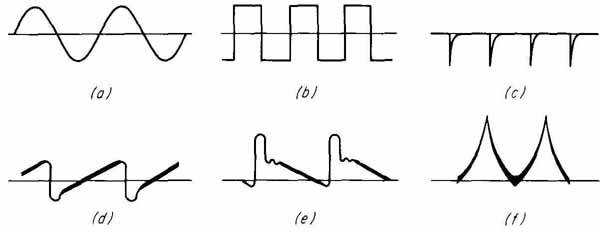
FIG. 19 Symbols of waveforms: (a) sine wave; (b) square wave; (C) trigger;
(d) through (f) complex forms.
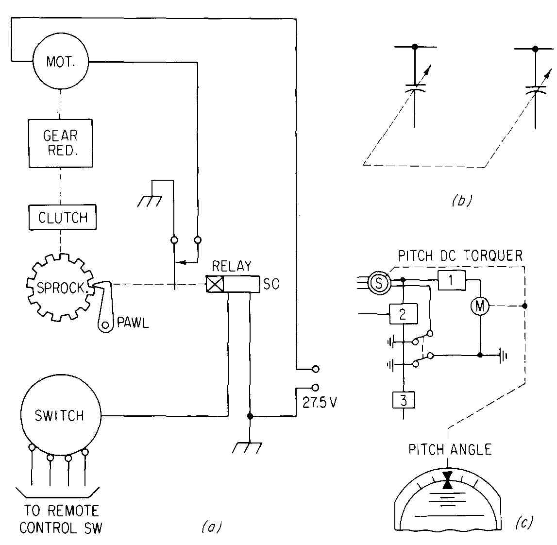
FIG. 20 Mechanical connections: (a) autopositioner; (b) ganged tuning
capacitors; (c) attitude indicator.
14. Separation and Interruption
It is often desirable to show a separate package apart from the rest of the circuit or system. For instance, if the same package (or pack as it is sometimes called) is to be used several times, it may be drawn as blocks instead of as a schematic diagram. In such a scheme, the schematic diagram would have to be drawn once, but only once. In FIG. 21 three ways of drawing a pack schematically, using different terminal or interruption techniques, are shown. FIG. 21 d shows how the pack might be drawn diagrammatically as a block. FIG. 21 a shows the circuit as removed at terminals. FIG. 21 b simply encloses the pack with an optional enclosure line but does nothing about the terminals. (In all four figures, the lines, or terminals, have been identified by means of numbers.) FIG. 21 c shows another method of separating a package. While this is a fairly widely used method, it is slightly confusing. The V-shaped lines at the end of each conductor do not represent any specific kind of connection in this scheme. Yet ANSI/IEEE Y32E uses this symbol to show a male contact. It is so used in other drawings in this guide, especially in Section 10. The Vs, incidentally, are not supposed to be arrowheads. They are correctly drawn at a 90° angle.
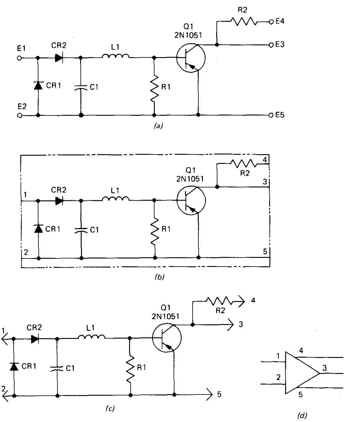
FIG. 21 Representation of a circuit package separated from the rest
of the system. (From ANSI Y14.15, “Electrical and Electronic Diagrams.”)
FIG. 22 illustrates other ways of interrupting groups of lines. Lines are generally grouped together in threes. If there are more than three lines to be shown, groups should be separated, as at the right in FIG. 22a. Spacing between lines should be a minimum of+ in., and between groups - in. Brackets may be joined by means of dashed lines, as in FIG. 22b. FIG. 22c shows hypothetical uses of circuit-return symbols. If the inverted triangle is used, letters and general notes ( FIG. 22d) will probably be necessary. The chassis symbol and the first triangle (with letter F) serve the same purpose, and either one could be used. These symbols are usually oriented as shown here. If it is more convenient, they can be drawn at the ends of lines extending upward or to the right or left. In other words, the entire figure ( FIG. 22c) could be turned at 90 or 180 degrees from its present position. (Letters and numbers might be changed to read in a convenient manner, though.)
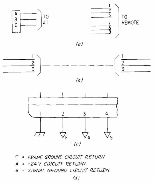
FIG. 22 Interruption and circuit return. (From ANSI Y14.1 5.)
FIG. 23 shows the schematic diagram for the preamplifier circuit of the Apollo moon camera. It is enclosed by the optional enclosure lines. The preamplifier is made up of discrete components, primarily to provide low-noise performance. The video signal from the camera is fed into the preamplifier. The no-dot system has been used.
The camera is 17 in. long, including a zoom lens, and weighs 13 lb. It generates a field sequential color signal using a single-image tube and a rotating filter wheel. A ground-station color converter later changes the sequential color signal to a standard NTSC color signal. In addition to the camera there is a small (85-cm viewfinder monitor for the astronaut and a transmitter. FIG. 2 shows the entire system in block form. The no-dot system has been used.
15. Schematics Using ICs and Other Components
Since the age of microelectronics began, there has been an evolution from drawing schematics with only discrete symbols to drawing schematics with IC symbols and discrete component symbols. As microelectronics is able to put more and more devices on an IC, it becomes totally impractical to show the schematic of an IC on an overall schematic. These schematics combining ICs and discrete symbols presume that one understands the function of the ICs used, just as one would have to know the function of a tube, for example. The following figures, together with FIG. 17, will show a few schematics containing ICs and some basic ideas on how to draw them.
FIG. 24 is a schematic of a two-phase clock for an 8080 microprocessor. This schematic uses discrete devices (resistor, capacitors, and a crystal) and ICs (NOR gates, buffers, and flip-flops). Actually, the NOR gates, the flip-flops and the buffers are each on one IC, respectively. Primarily, however, it is the timing diagram that we want to discuss when doing this type of schematic. Many digital circuit schematics utilize a timing diagram to show how the circuit works. The timing diagram can appear anywhere on the schematic, but the authors generally prefer it to be above or below its associated circuit, to make it easier to understand the circuit without having to look all over the diagram. In the circuit, the output of FF, output is half the frequency of the oscillator, 0, is the OR-inverted output of the oscillator and FF Gate 4 output 0, is buffered to TTL levels (5 V). 02 is the OR-inverted output of FF.
FIG. 25 is an 8-bit analog-to-digital converter. This circuit utilizes two AND gates with inverted outputs, an inverter, four ICs, and several discrete components. The overall schematic uses the dot system for connections. The IC pins are shown within the IC symbol. If the pin functions are to be shown, they should be shown inside the IC symbol and the pin numbers outside. Manufacturers’ model numbers are shown within the IC symbol, where it is preferred because there is less cluttering of the schematics. The voltage sources are not shown, which is generally typical for most schematics. The schematic flows from left to right with the analog input on the left and the digital output on the right. This circuit was used for teaching reasons and today it can be purchased on a single IC.
1. There are connections at points 9, 10, and 11.
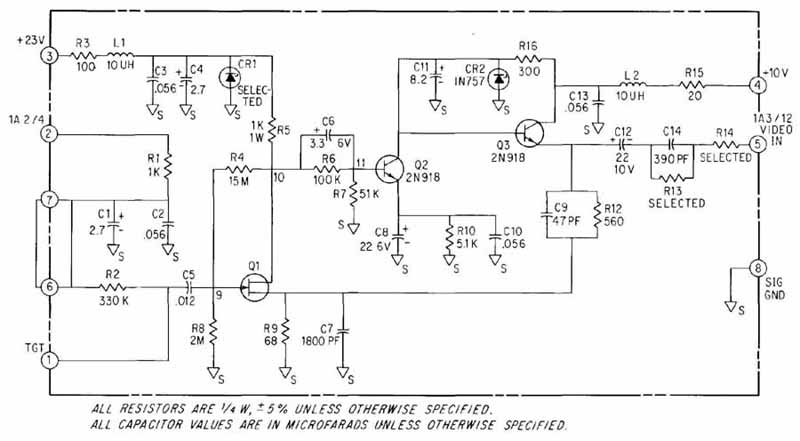
FIG. 23 Preamplifier circuit of Apollo television camera. (Westinghouse
Electric Corp.)
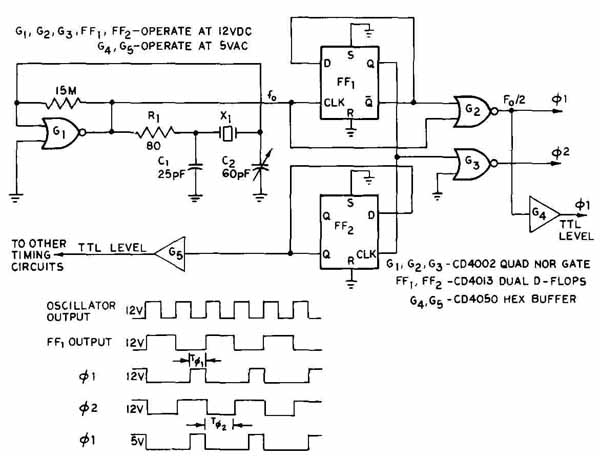
FIG. 24 Schematic diagram of a two-phase clock for an 8080 microprocessor.
(EDN Magazine, January 5, 1977, p. 50.)
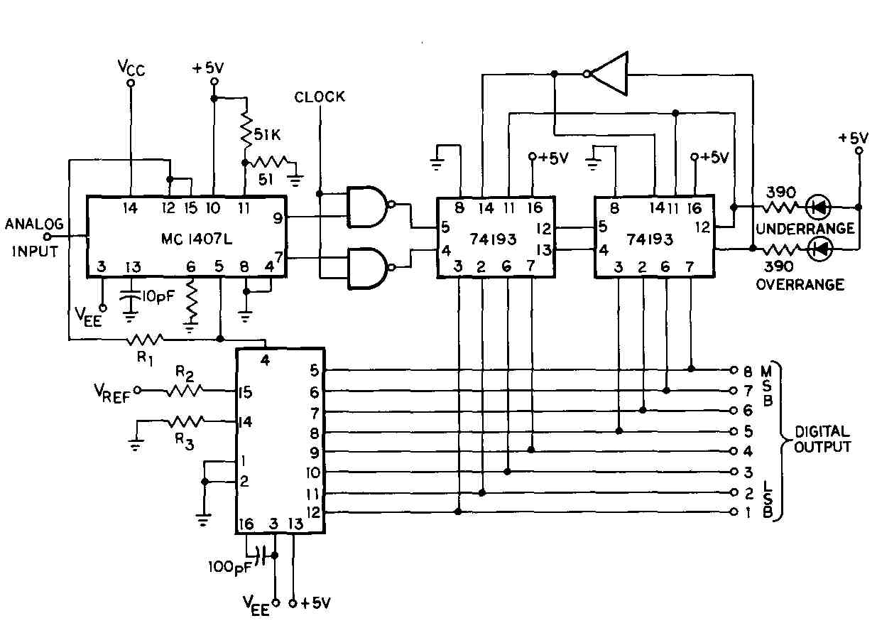
FIG. 25 Schematic diagram of an analog-to-digital converter (EDN Magazine,
June 20, 1975, pp. 118—120).
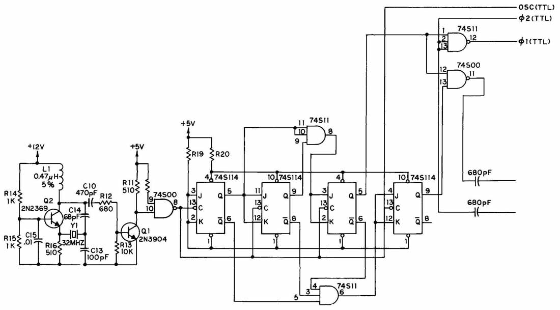
FIG. 26 Partial schematic diagram of a two-phase clock. (EDN Magazine,
September 20, 1975, pp. 53—55.)
FIG. 26 is a partial schematic of a two-phase clock for an 8080 micro processor. This schematic is an example of how the functions are shown within the symbol of the ICs (J-K flip-flops) and the labeling of the pin numbers outside the IC symbol. The IC manufacturer’s model number is shown outside the IC symbol. The schematic flows from left to right with oscillator on the left and the clock outputs on the right.
16. Hybrid Diagrams
Hybrid diagrams are just that; they can contain schematic diagrams, logic diagrams, wiring diagrams, pictorial drawings, mechanical connections, and pneumatic connections.
FIG. 27 is a hybrid diagram combining most of the aspects of a hybrid drawing, including a schematic, wiring information, logic circuitry, and mechanical devices and their associated interconnections to electrical devices. Approximately the left third of this diagram contains a schematic. The uppercenter portion contains a pictorial view of a gyroscope and its mechanical connection to the various synchros. The diagram also contains logic gates (e.g., flag logic) and a schematic of the flag logic circuit. Along the right side of the diagram, there is wiring information showing the wire numbers connecting the jack pins. The reader will notice a loop-like symbol of lines 49 through 51. This indicates that the three wires are twisted together. Somewhat below this is a similar symbol which indicates that wires 45 and 46 are twisted together and shielded.
SUMMARY
The schematic shows by means of graphic symbols the functions and connections of a specific circuit arrangement. Symbols for use in such a diagram are extensively covered in ANSI/IEEE Y32E and IEC Publication 117, and the preparation of the diagram itself is covered by ANS Y14. 15. There are certain basic arrangements of transistors and tubes which are usually repeated in electronics circuit diagrams. With these and some types of interstage coupling, certain patterns are often discernible—usually early in the game, when one starts to plan an elementary diagram. Designation, or referencing of each component part of a circuit, is important. Certain standard abbreviations and prefixes are used for this purpose. Sufficient space must be made available near each component for referencing.
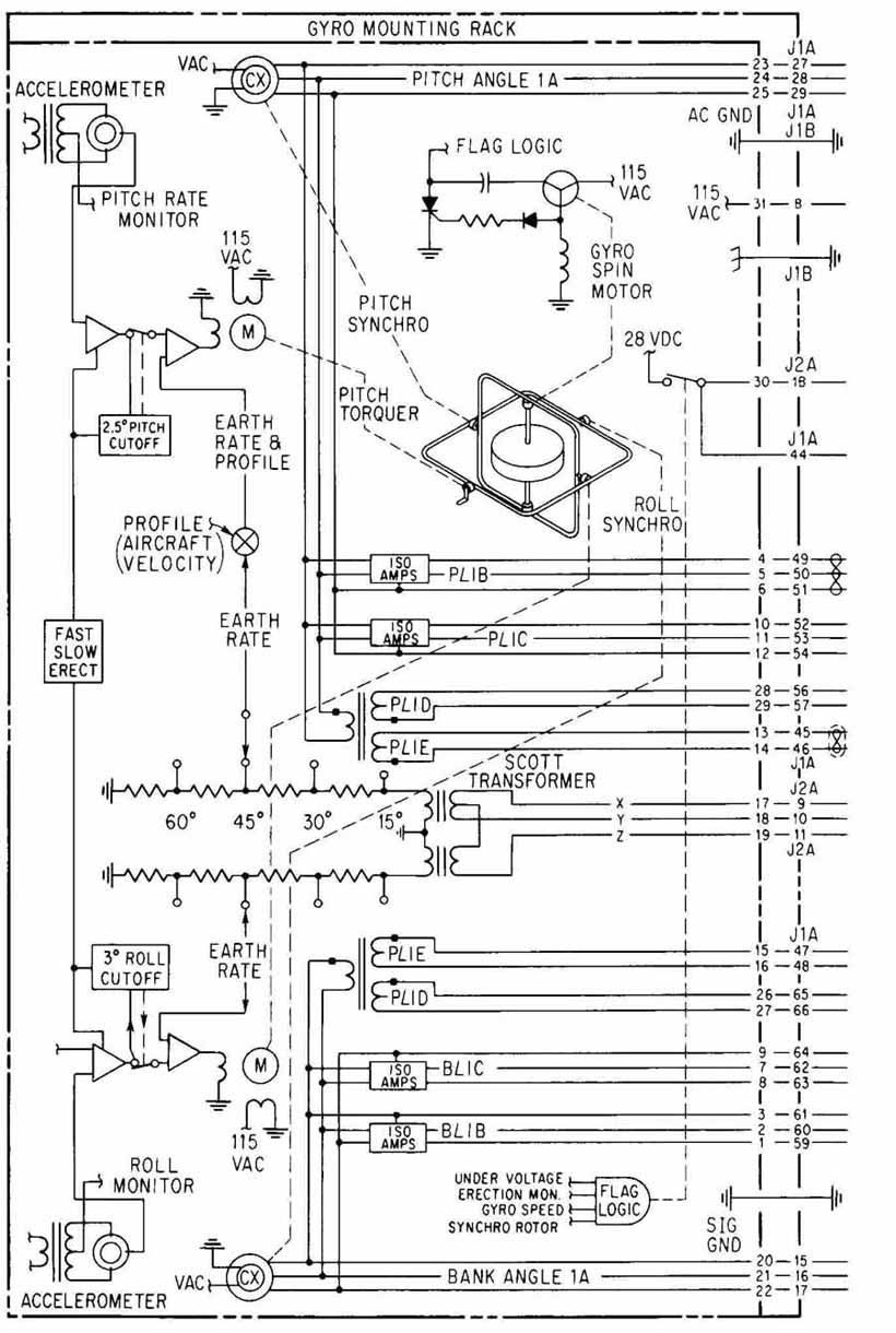
FIG. 27 Part of a system schematic of an aircraft altitude system.
This is a hybrid drawing. (Douglas Aircraft Co.)
Conventional treatment is sometimes employed to eliminate the drawing of certain lines in order to avoid cluttering in a drawing. On the other hand, additional material, such as general notes and data on waveforms, is often added to a schematic diagram. A symbol is generally spaced midway along the span of circuit path on which it is drawn. Mechanical connections must be shown at times. Certain patterns are usually followed in laying out certain types of circuits in diagrammatic form. Radio circuits, for example, usually follow a cascade arrangement in which the signal path goes from left to right and the transistors are aligned horizontally. Auxiliary circuits, such as power circuits, are generally placed in the lower part of any schematic diagram. In circuits with ICs, the signal flow is generally left to right. However, due to multiple sections or functions on a single IC and several Iqs within a circuit, there may be some “doubling back” to connect to a function/of a previous IC. Overall balance and symmetry are other concepts that are observed in diagrammatic layout.
QUESTIONS
1. What set of standards governs the preparation of schematic diagrams?
2. In what way, or ways, is a schematic diagram different from a connection diagram?
3. How would you show the value 100,000 on a circuit drawing? 150,000 pF?
4. To what sort of elements do the following terms refer:
a. 12AV6
b. Z
c. 50K
d. 2N329
e. CR
5. What is meant by the term density as it applies to schematic diagrams?
6. What is meant by the term symmetry as it applies to schematic diagrams?
7. Where should timing diagrams go on IC schematics?
8. For what purposes are schematic diagrams used?
9. Where are auxiliary circuits normally placed on the schematic diagram?
10. If a resistor is positioned on a vertical line (signal path), where would you place its identification?
11. Where would you place the identification for a vacuum tube in a schematic diagram of a circuit having cascade projection?
12. What letters are used to identify the three leads of a MOSFET?
13. What elements are often found in a hybrid diagram?
14. What do the parallel lines adjacent to the outline of a picture-tube symbol represent?
15. Define the prefixes micro-, milli-, kilo-, and mega-.
16. Is it possible to draw a schematic diagram using only one width of line and in so doing comply with the standards?
17. If you are assigned to make a finished drawing of a schematic diagram of a circuit, in what form is the information to which you will refer apt to be?
18. When an IC has both pin functions and numbers, where should each go?
19. What methods are used in coupling different stages together? (Name three.)
20. In what way may the number of connecting lines in a diagram be reduced?
21. What two shapes are generally used for IC modules?
22. State briefly, or use sketches to show, how you would separate a package from the rest of a circuit.
23. What is the difference between a picofarad and a micro-micro-farad?
24. In which direction should the signal flow in a schematic?
25. What is the preferred method of where to show the IC manufacturer’s model number in relation to the IC?
26. What types of drawing are found on a hybrid diagram?
PROBLEMS
1. Draw the schematic diagram of the all-channel CB monitor-receiver shown in FIG. 28. Use standard identification for each component. We have shown capacitor C (10 pF) at the upper left. Each capacitor and resistor should have a similar reference designation.
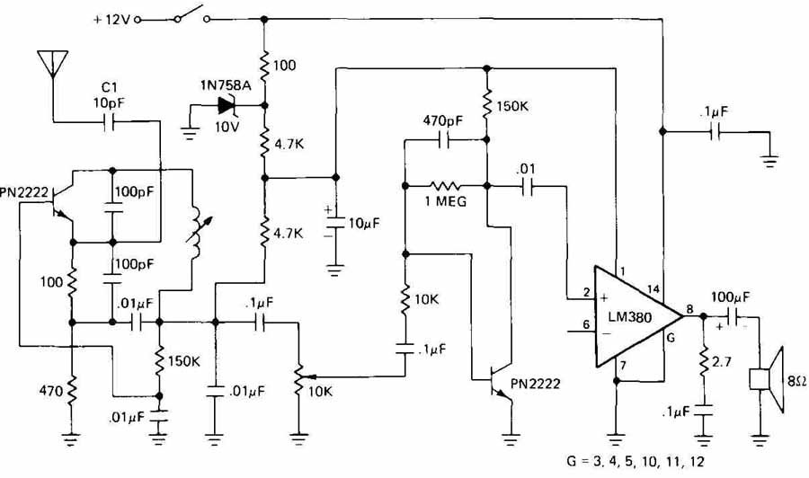
FIG. 28 ( Prob. 1.) Schematic diagram of CB monitor receiver. (Kantronics,
Inc.)
Make any changes or improvements in the symbols or designations and values of components that you think would be appropriate. Add a suitable title and the following note: Unless otherwise specified all resistors are ± 5%, W. There is no connection at pin no.6 of the amplifier LM 380. If well planned, this diagram, with a suitable title, will fit on an 8- X 11 sheet.
2. Draw the schematic diagram of a digital clock that is shown in FIG. 29. This will fit on an 11 X 17 sheet. Complete the drawing by showing resistors R through R and drawing the CRB 1 full-wave bridge where indicated. Use ANSI practice in identifying the following components:
The corner pins are numbered on the Mostek clock chip. There are no connections to pins 13 through 17. The coil symbol at the left is part of trans former T which has an iron core. The leads from the left winding of the transformer go to the 115-v ac supply.
3. Complete the schematic diagram in FIG. 30 by insertion of the correct symbols as indicated by standard notation. Add the identification of each component and the capacity if given below. Squares Z Z etc., are integrated circuits drawn as squares or rectangles with identification shown within the square. Video input is at 12. The letter U may be substituted for Z.
This drawing will be slightly crowded on 8.5 X 11 paper and will have more than enough room on 11 X 17 paper.
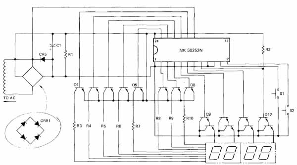
FIG. 29 ( Prob. 2.) Schematic diagram of a digital clock.
4. Complete the schematic diagram of the four-function calculator shown in FIG. 31. Major elements are the terminal (at top) that connects to the LED strip (not shown), the calculator chip TMC 972, and the keyboard module. The unfinished leads should be completed by drawing lines horizontally and/or vertically to the connector indicated. Use 11 X 17 paper. Use the standard battery symbol. Show stub lines at NCs (no connections).
5. Referring to FIG. 32, fill in the IC symbol with four 2-input, distinct- shape NAND gate symbols plus zero voltage and the positive voltage:
Pins 1 & 2 Pin 3 Pins 4 & 5 Pin 6 Pin 7 Pin 8 Pin 9 & 10 Pin 11 Pin 12 & 13 Pin 14 |
Inputs to NAND gate 1 Output of NAND gate 1 Inputs to NAND gate 2 Output of NAND gate 2 Zero voltage reference Output of NAND gate 3 Inputs to NAND gate 3 Output of NAND gate 4 Inputs to NAND gate 4 Positive voltage reference (+ 5 V) |
6. Redraw the high-fidelity amplifier shown in FIG. 18 to about 2+ or 3 times the size that it appears in the guide. Instead of the component identification system shown, use the ANSI system of identification shown in this section. Use 11 X 17 or 12 X 18 paper.
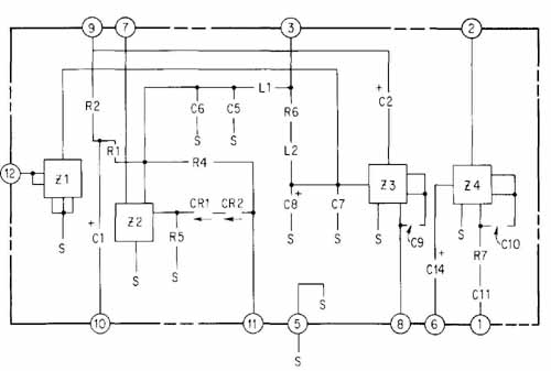
FIG. 30 ( Prob. 3.) Post-amplifier of a moon-walk television camera.
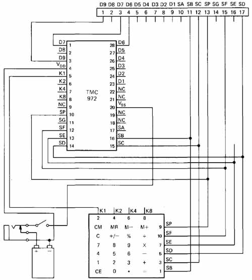
FIG. 31 ( Prob. 4.) Schematic diagram of a four-function calculator.
(Texas Instruments, Inc.)
FIG. 32 ( Prob. 5.) A four 2-input NAND-gate IC.
7. Redraw the schematic diagram shown in FIG. 33 to approximately twice the size it is shown in the guide. Use standard identification for resistors, capacitors, etc. Add the following information on or near ICs 1 and 2: Pin 1, Trigger; 2, REF; 3, R/C; 4, GND; 5, Y±; 6, C; 7, E; 8, LOGIC. On IC 3: Pin 1, CL; 2, D; 3, CLOCK; 4, GR; 5, Q; 6, Q. Use 8 X 11 paper.
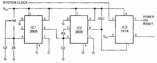
FIG. 33 ( Prob. 7.) Schematic diagram of a power on reset circuit.
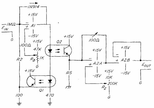
FIG. 34 ( Prob. 8.) An isolation circuit with optical couplers.
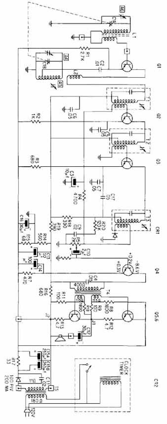
FIG. 35 ( Prob. 9.) Schematic diagram of a transistor clock radio.
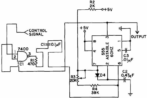
FIG. 36 ( Prob. 10.) An unorganized schematic diagram of a VTR clock.
8. FIG. 34 is a freehand sketch of an isolation circuit that is not complete. Make an instrument drawing of this circuit that is complete, uses correct symbols in accordance with ANSI/IEEE Y32E, and has maximum identification of components. In the circuit, Q and Q are optical couplers, FCD 810 or equivalent, A and A are operational amplifiers (A is separated into two parts, A, and A2B), RB is a bias resistor, and R is a zero-adjust potentiometer. (R and R are 100 k each.) Make any corrections which appear to be appropriate. Use a standard termination scheme for EJN and E This problem will fit on 8.5 X 11 paper; 11 X 17 paper would also be OK.
9. Make a drawing of the clock-radio circuit shown in FIG. 3 5. Correct the symbols where obsolete or incorrect ones appear. Add identification for semiconductors as follows: Q converter, 95101; Q first IF, 95103; Q second IF, 95102; CR detector, IN295; Q audio driver, 95201; Q and Q audio outputs, 95220; CR rectifier, 1N290. All resistors are - W. The no-dot system has been used except at connections J and J Resistance values are in ohms unless otherwise noted, and all capacitance values are in microfarads. Use 11 X 17 or 12 X 18 paper.
10. Rearrange the unorganized schematic of a video-tape-recording (VTR) clock ( FIG. 3 6) so that it is in a logical systematic order with the input on the left and the output on the right.
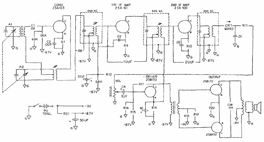
FIG. 37 ( Prob. 11.) Incomplete sketch of a six-transistor AM receiver.
11. FIG. 37 is a sketch of a six-transistor radio-receiver Circuit. Many symbols are missing, but clues to their identity are given as reference designations or values. All transistors are PNP; their collector and emitter leads are identified. Capacitors at A and A are variable; no values are available. Capacitors in 455 kHz (KC is an older term) packages also have no values. Other capacitances are given as microfarads (uF) unless otherwise shown. Resistance values not already shown are as follows:
Some symbols are incorrectly shown. Reference designations may not be in the best sequence. Correct and complete the schematic diagram of this circuit, using the standard symbols and reference-designation procedure. Use 12 X 18 paper or larger.
12. FIG. 38 is the incomplete schematic diagram of a circuit that indicates at a remote location what the status of a telephone line is. LED T 1 L209 is dark when the line is not in use, on when the line is in use, and flashes when the phone is ringing. Complete the schematic by showing standard symbols for discrete elements and distinctive shapes for the logic elements. Elements should be properly identified. MCT-2 is an optical coupler. This is a tight fit on 8.5 X 11 paper.
13. FIG. 39 is a sketch of the logic diagram and schematic diagram of a flip-flop circuit. Make a complete instrument drawing of this sketch, improving symbology or layout wherever you think it is advisable. Add the following information: total capacitance, 115 pF; total resistance, 70 k tunnels (cross over paths), 14; V pin no. 3; Gnd, pin no. 8. Use 11 X 17 or 12 X 18 paper.
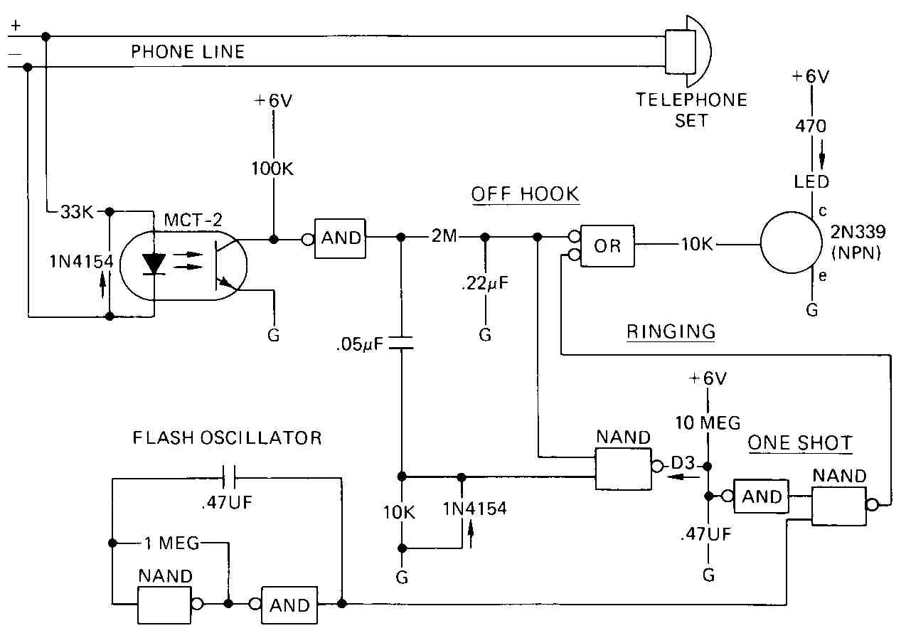
FIG. 38 ( Prob. 12.) A logic diagram and schematic diagram of an integrated
semiconductor flip-flop circuit. (Circuit from Texas Instruments, Inc.)
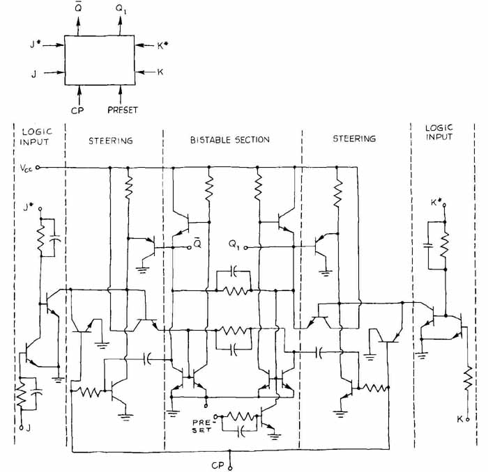
FIG. 39 ( Prob. 13.) A block diagram and a schematic diagram of an
IC flip-flop circuit. (Texas Instruments, Inc.)
14. FIG. 40 shows an incomplete sketch of a satellite beacon oscillator. Many symbols are missing or incorrect, but clues are present as to their correct identities and values. All transistors are PNP; their emitter and collector leads are identified. Capacitors are identified as C C or with symbols, some obsolete or nonstandard. Complete the schematic diagram insofar as possible using standard symbols and reference designations.
Some values are … Use 11 X 17 or 12 X 18 paper.
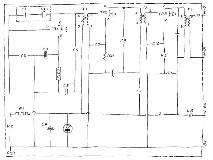
FIG. 40 ( Prob. 14.) Schematic diagram of an oscillator for a communications
satellite. (Rough sketch.)
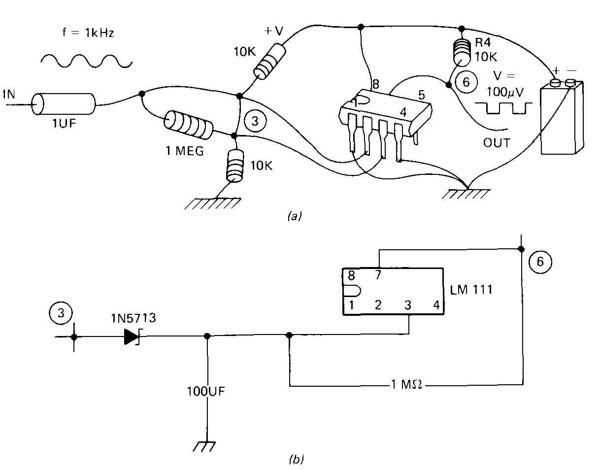
FIG. 41 ( Prob. 15.) Integrated-circuit comparator used as a clipper:
(a) pictorial diagram; (b) partial schematic diagram.
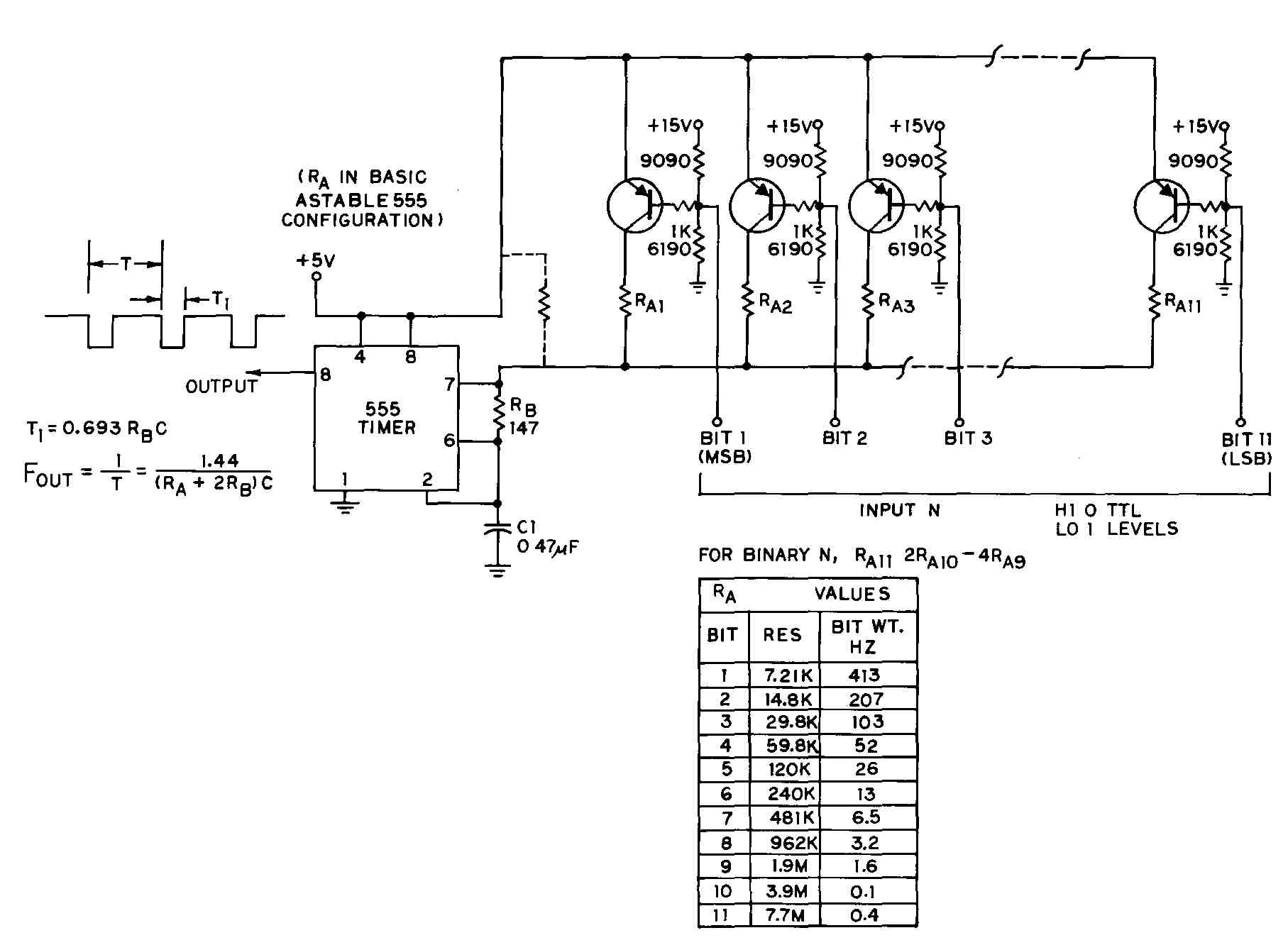
FIG. 42 (Prob. 16.) Schematic diagram of a pulse generator. (EON
Magazine, August 20, 1974, p. 92.)
15. FIG. 41 has a pictorial view of an IC comparator circuit used as a clipper in a. An improvement to that circuit including a Schottky diode is shown in b. Make a complete schematic diagram of the improved circuit, including waveforms. Use 8 X 11 paper.
16. FIG. 42 is a schematic of a programmable pulse generator; however, bits 4 through 10 are missing. Complete the schematic on 11 X 17 paper, adding the missing bits and the values of all the timing resistors.