AMAZON multi-meters discounts AMAZON oscilloscope discounts
One of the most fantastic and far-reaching developments of the twentieth century is that of microelectronics. It began in 1948 with the transistor and continues to grow and evolve at a phenomenal pace. It has made a new industry and many new manufacturing companies and has brought about a new technology in which graphics plays an important part. In this Section the authors will show some of the drawing that is involved and some of the background that surrounds it.
1. Types of Integrated Circuit
An integrated circuit is a circuit in which devices of several to thousands of different types, such as capacitors, resistors, and transistors, are made on a single piece of material such as a small silicon chip and then connected to form a circuit.
FIG. 2 lists the types of integrated circuit that have been developed to this point in time. Typical of many of these circuits is the wafer ( FIG. 1), which includes many dice, each of which bears an individual integrated circuit (IC) chip. If we exclude the hybrid ICs for the moment, we notice that there are two fundamental processes, bipolar and metal-oxide semiconductor (MOS). The glossary that follows briefly describes the differences and variations among the processes shown in FIG. 2.
Bipolar: One of two fundamental processes for fabricating ICs and currently the more popular. A bipolar IC is made up of layers of silicon with differing electrical characteristics. Current flows between the layers when a voltage is applied to the “junction,” or boundary between the layers.
TTL: Transistor-transistor logic, by far the most successful bipolar IC logic. It gets its name, as do other digital IC product families, from the way the components are combined to form the logic elements. Digital ICs solve problems by manipulating electrical signals that represent bits of information. Basic TTL is a mature product, but faster and lower-power versions are extending the life of TTL into the 1980s.
ECL: Emitter-coupled logic, a bipolar IC family that uses a more complex design than TTL to speed up IC operations. It is costly, power-hungry, and difficult to use, but it could become important in the next generation of large computers because it is four times faster than TTL.
IIL. Integrated injection logic, a high-density bipolar logic design. It holds promise of producing ICs with a circuit density approaching MOS, the speed of TTL, and the low power requirements of CMOS.
MOS: Metal-oxide semiconductor is the second fundamental process for fabricating ICs and the fastest growing. The active area of a MOS chip is at the surface, where a gate electrode applies a voltage to a thin layer under it to create a temporary “channel” through which current can flow.
PMOS: The oldest MOS circuit technology uses a channel of P-type material, where the flow of current is made up of positive charges.
NMOS: The N-channel MOS, where the flow of current is made up of negative charges. It is two to three times faster than PMOS circuits.
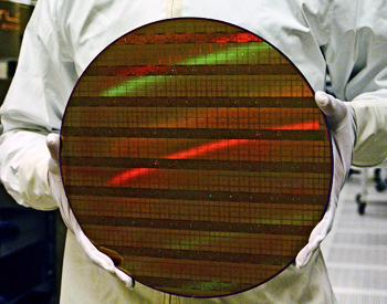
FIG. 1 Partial view of a wafer on which many microchips have been fabricated.
(Intel Corporation.)
CMOS: Complementary MOS combines P- and N-channel transistors to create an IC that is as fast as a NMOS circuit but consumes very little power.
OTHER MOS: Variations of the MOS process are being developed. High-performance MOS (H-MOS) is one example. Transistors built on the slanting surface of a V groove (V-MOS) constitute another example.
2. Transistors, the Basic Building Block
Although this is not a guide on electronic theory, FIG. 3 is a diagram of several transistors or transistor-like devices. The original bipolar PNP or NPN transistor has acquired some companions, but they are basically made of the same material, silicon being the most widely used. To enable the crystal to conduct electric current, small quantities of impurities are mixed with the pure silicon. If phosphorus is added, N type is the result. If boron is added, P type is produced.
By itself neither N- nor P-type material can accomplish a junction. But, when put together in various combinations and configurations, they provide a number of practical working semiconductor devices. It is the behavior of electrons and holes in the vicinity of the PN junction that gives bipolar junction transistors their unusual properties. In MOS transistors (MOSFETs), however, the active area is at the surface. The silicon controlled rectifier (SCR) is widely used in the electric-power and industrial fields and is discussed at more length in Sections 9 and 10.
Transistors are still widely available and used as discrete components. Along with diodes, capacitors, and resistors, they can be made to be part of an integrated circuit. A summary of semiconductor devices follows.
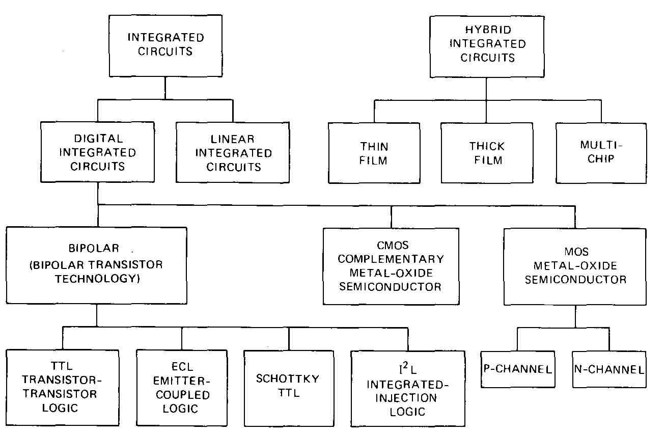
FIG. 2 Types of integrated circuit.
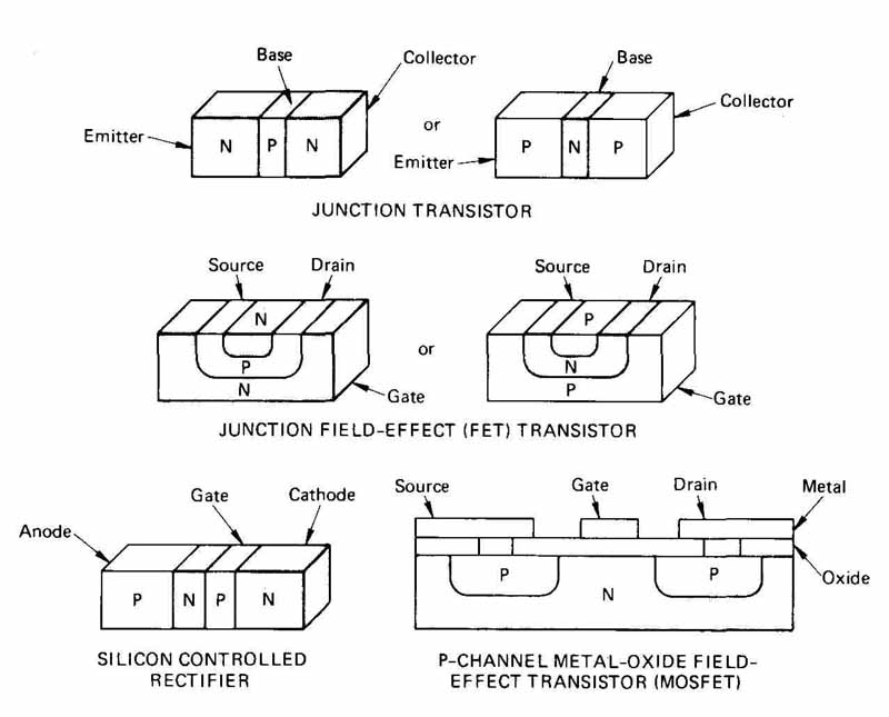
FIG. 3 Some basic semiconductors. From top to bottom: junction transistors,
junction field-effect transistor (JFET), silicon-controlled rectifier
(SCR), and MOS field-effect transistor.
1. Thyristors
- Silicon controlled rectifier (Electrically controlled switch for dc loads.)
- Triac (Electrically controlled switch for ac loads.)
2. Diodes (Exhibit very high resistance to current flow in one direction and little resistance in the other.)
3. Discrete transistors (Three-terminal devices used for amplifying or switching electrical signals.)
- Bipolar
- FET (field-effect transistor) Unijunction
4. Charge-coupled devices (CCDs) (Storage devices in which packets of electric charge are moved across the surface of a semiconductor by electrical signals.)
5. Photo-semiconductors (Emit or absorb electromagnetic radiation, usually in the visible or infrared band.)
- Phototransistor LED (light-emitting diode)
- Photo-thyristor
6. Integrated circuits (To be defined and discussed later.)
7. Hybrid integrated circuits (To be defined and discussed later.)
JUNCTION TRANSISTOR
3. An Integrated-Circuit Processing Glossary
In describing the manufacture of ICs, we believe that presentation of the following terms will make it easier for the reader to understand the processes.
Alignment: A technique in the fabrication process by which a series of six to eight masks are successively registered to build up the various layers of a monolithic device. Each mask pattern must be accurately referenced to or aligned with all preceding mask patterns.
Die: A portion of a wafer bearing an individual IC, which is eventually cut or broken from the wafer. (The plural is dice.)
Diffusion: A high-temperature process involving the movement of controlled densities of N-type or P-type impurity atoms into a solid silicon slice in order to change its electrical properties.
Emulsion: A suspension of finely divided photosensitive chemicals in a viscous medium, used in semiconductor processing for coating glass masks.
Etching: A process using either acids or a gas plasma to remove unwanted material from the surface of a wafer.
Mask: A chrome or glass plate having the transparent circuit patterns of a single layer of a wafer. Masks are used in defining patterns on the surface of a resist-covered wafer.
Master mask: A chrome mask of a complete wafer’s multiple images. It is used either in projection printing on a wafer or to contact-print additional masks.
Photoresist: A material that allows selective etching of a wafer when the wafer is photographically exposed. With a negative resist, the resist film beneath the clear area of a photo-mask undergoes physical and chemical changes that render it insoluble in a developing solution. In a positive resist, the same areas after exposure are soluble in the developing solution, so they disappear, permitting development of the exposed pattern underneath.
Reticle: A glass-emulsion or chrome plate having an enlarged image of a single IC pattern. The reticle is usually stepped and repeated across a chrome plate to form the master mask.
Step and repeat: A method of positioning multiples of the same pattern on a mask or wafer.
Stripping: A process using either acids or plasma to remove the resist coating of a wafer after the exposure, development, and etching steps.
Yield: The number of usable IC dice (chips) coming off a production line divided by the total number of dice going in. Yield tends to be reduced at every step in the manufacturing process by wafer breakage, contamination, mask defects, and processing variations.
4. Integrated-Circuit Fabrication Process
FIG. 4 shows the major milestones of the silicon IC fabrication process. Our description will begin at step 2, in which the crystal has been sawed into thin wafers which have been lapped and polished to a mirror-like finish with no scratches or defects. Next, a layer of silicon dioxide (Si0 is grown on the surface to protect it from contamination and prevent the diffusion of impurities in some of the processes that follow.
The next step is to provide “windows” through which impurities can be deposited on the surface. Special photolithographic techniques are used to remove the oxide in certain selected regions. When the wafer is placed in a diffusion furnace at 1000 degr. C and a gas containing the required impurity is passed over the surface, the impurities are deposited where there are windows and then are “diffused” into the silicon. This buried layer reduces the series collector resistance of transistors. Table 1 shows the masks that are used in the basic fabrication techniques. The windows mentioned above have been made using mask 1.
After the buried-layer diffusion is complete, the Si0 is removed from the wafer surface and a new layer of N- or P-type silicon is grown on the surface by means of epitaxial growth. In this step the wafer is exposed to an atmosphere containing a silicon compound at high temperature, and a new layer of silicon atoms is deposited in accordance with the crystal structure of the substrate. This epitaxial layer is also doped by including small amounts of the desired impurity in the gas stream during its growth.
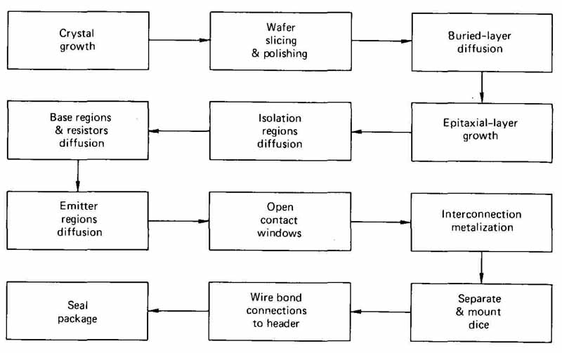
FIG. 4 The steps in the manufacture of a silicon integrated circuit.
(From D. J. Hamilton and W. G. Howard, Basic Integrated Circuit Engineering,
McGraw-Hill Book Co., New York, 1975.)
TABLE 1 The Basic Fabrication Sequence and Masks Required
As shown in Table 1 and FIG. 4, successive oxide growths, photolithography steps, and diffusions are undertaken to provide base and emitter regions, isolation walls, etc. The last steps include making windows for interconnections among the many devices now present on each circuit, followed by the metallization process. In this process a metal, often aluminum, is evaporated over the surface of the wafer; then unwanted portions are etched away and the interconnection contacts are left.
Finally the wafer is broken up into small dice, or chips, each having a single circuit or assembly, such as a microprocessor. Each chip is then mounted on a header, such as a dual-in-line mounting, and the aluminum contacts are connected to the header leads or pins by wire or one of the newer processes, such as film striping.
5. Photolithography
This process accomplishes two important functions: (1) reduction of the original mask drawing to the final mask size and (2) the photoresist process itself. The process of reducing the mask size also includes producing multiple images of the layout.’
The photoresist process involves making windows in the Si0 layer of the wafer. The photoresist is a light-sensitive coating that is placed over the oxide. The glass mask with the desired portion of the circuit pattern is placed over the photoresist. After exposure to ultraviolet light, the unexposed coating is dissolved; that which remains is chemically resistant to the solution or gas that is used to etch away the oxide. Later the remaining photoresist can be removed, so that additional masking and etching can be performed. The process is illustrated in FIG. 5.
FIG. 6 includes, greatly enlarged, three steps of the diffusion process as they would appear if one were looking at the surface of an IC. (In other circuits, the shapes of these components may be different from those shown in FIG. 6.)
6. Drawing and Artwork for IC Design
Integrated circuits can be classified by the number of logic elements or “gates” they contain. Small-scale integration (SSI) refers to chips that have 100 or fewer gates. Medium-scale integration (MSI) refers to chips containing 100 to 1000 logic gates, while large-scale integration (LSI) refers to chips with more than 1000 elements. Very-large-scale integration (VLSI) includes any module that has more than 50,000 or 100,000 gates. FIG. 7 shows the first mask of a series for an SSI. As shown in FIG. 8, this chip has 31 elements.
Many identical circuit chips are made from one wafer ( FIG. 1).
(a) Initial coating
(b) Contact printing
(c) After developing
(d) After oxide etching
(e) After stripping
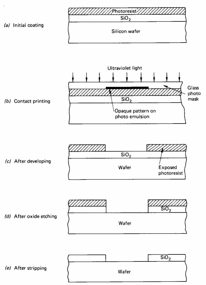
FIG. 5 Steps in the photoresist process. (From D. J. Hamilton and W.
G. Howard, Basic Integrated Circuit Engineering, McGraw-Hill Book Co.,
New York, 1975.)
The nature of IC design is such that devices may have different shapes in different circuits. Some other shapes are shown in FIG. 9. FIG. 10 shows a series of masks for a latch circuit which is part of a microprocessor chip. The schematic diagram of this circuit is shown in FIG. 11, and the photograph of the LSI microprocessor chip that contains the latch is shown in FIG. 12.
The original drawing for the mask shown in FIG. 7 was drawn to a scale 150 times the actual size. Notice the grid system that is used to facilitate accuracy. Spacing between components is actually as close as 0.0005 in. at times; therefore, alignment errors cannot exceed a few ten-thousandths of an inch. Such accuracy is usually obtained only with computer-generated drawings. The actual size of the SSI chip (Figs. 7 and 8) is about 0.125 (3.2) X 0.250 in. (6.4 mm). It is in the form of a flatpack package with 14 external leads.
Original drawings for LSI chips such as the microprocessor are often drawn 500 times the actual size. The TMS 9900 microprocessor was produced using N-channel silicon-gate MOS technology. The MOS devices can be made with very small geometry, permitting high densities. For example, the memory space of the 9900 is 65,536 bytes (where one byte = eight binary units). Only a small part of the drawing for the entire unit is represented by the latch artwork ( FIG. 10). The microprocessor is housed in a ceramic dual-in-line package 0.90 (23) X 3.20 in. (81 mm) and having 64 pins.
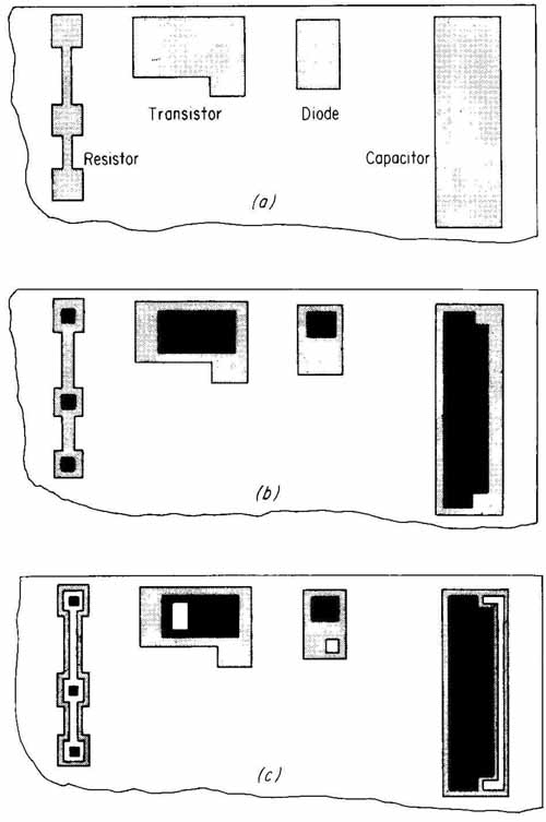
FIG. 6 Three steps in the manufacturing process of IC devices.
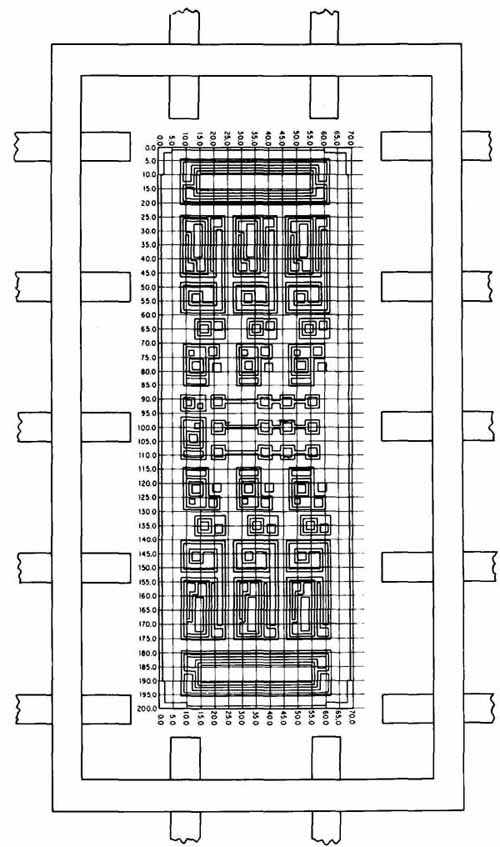
FIG. 7 The first of a series of drawings for the manufacture of an
integrated circuit. Greatly enlarged. (Texas Instruments, Inc.)
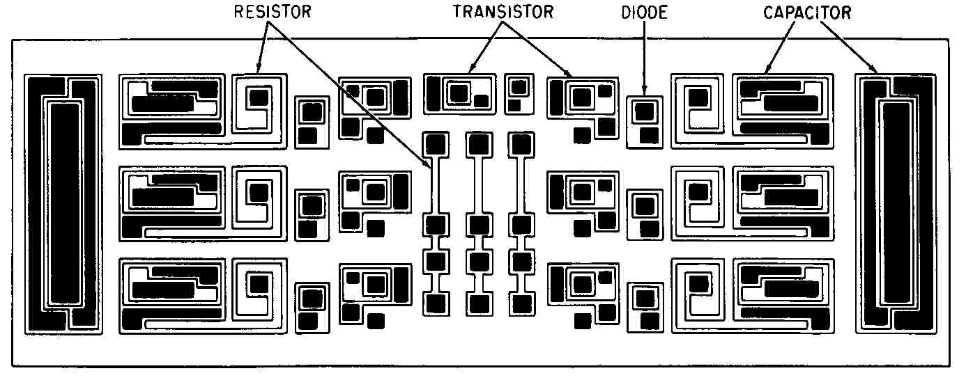
FIG. 8 The integrated circuit, greatly enlarged, (see FIG. 7) will appear
about like this after several diffusion processes. (Texas Instruments,
Inc.)
We have enlarged the lower left portion of FIG. 10 in FIG. 13. The metal-oxide transistors are shown at 2 and E and at 5 and G, and the small section shows separation of the metal and diffused parts with gate oxide in between. Unfortunately the transistor symbols in FIG. 11, although used considerably, are not standard. In FIG. 14 we have shown two of these symbols at a and c and the standard symbols at their right. Not only are the symbols not standard, they do not have arrows indicating whether they are N or P type. This doesn’t seem to bother the people who work with these diagrams day in and day out. But it is confusing to many who are not involved with the design and manufacture of these circuits.
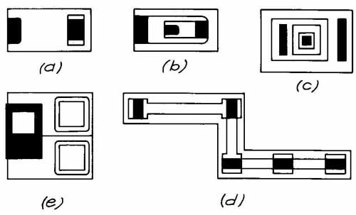
FIG. 9 Patterns of several elements after diffusion processes: (a)
PNP transistor; (b) NPN transistor; (c) lateral NPN transistor; (d) resistor;
(e) photonic IC with photodiode and transistors.
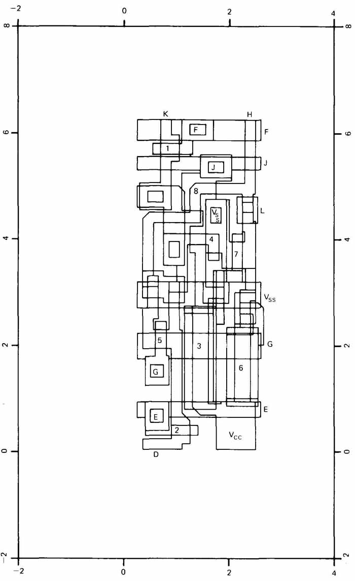
FIG. 10 The composite artwork for a latch circuit which is part of
a microprocessor. (Texas Instruments, Inc.)
LATCH CIRCUIT SCHEMATIC
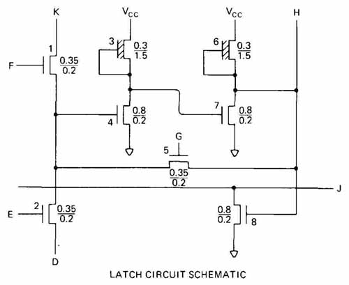
FIG. 11 The schematic diagram of the latch circuit shown in FIG. 10.
(Texas Instruments, Inc.)
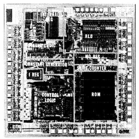
FIG. 12 Photograph of the TMS 9900 microprocessor greatly enlarged.
Latch circuits, which are flip-flop units, are part of the register (REG)
circuits. (Texas Instruments, Inc.)
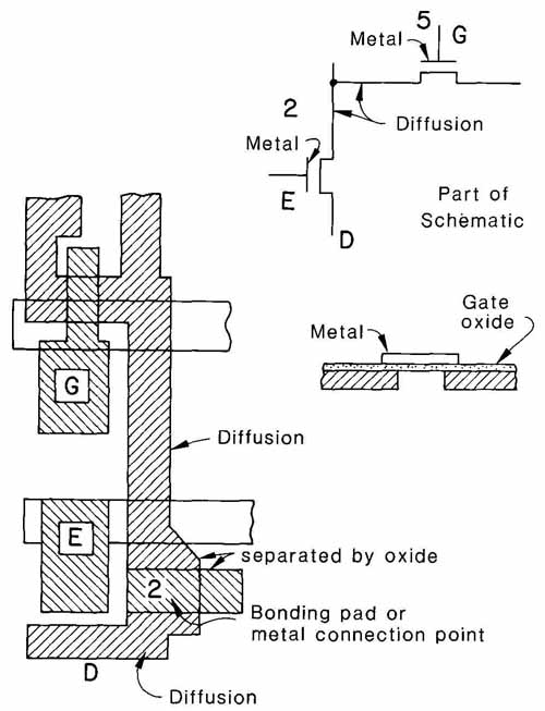
FIG. 13 Details ol the MOS latch circuit shown in Figs. 10 and 11.
(Texas Instruments, Inc.)
Artwork is made from each drawing on a plastic material called Rubylith. Cuts are made in this material — Mylar with a red plastic coating — and the coating is peeled off in the desired places. When the Rubylith artwork is photo graphed, the red areas will appear opaque to photographic film. The photograph looks pretty much like a negative.
In order to check the accuracy of medium- and large-scale IC drawings, debugging plots composed of all masks are made. Carefully following registration, the masks are superimposed on one another. Unwanted overlapping or less-than-minimum clearances can usually be seen.
Finally, to connect the elements of the circuit to their respective leads or other components (or both, in some cases) an aluminum pattern must be placed over the surface and in contact with the appropriate component. After openings for ohmic contacts have been made (mask 6 in Table 1 and step 8 in FIG. 4), the metal is evaporated over the entire surface of the wafer (step 9, mask 7), where it makes good contact with the silicon. The pattern could resemble that shown in FIG. 15. Unwanted metal is etched away, and the chip is ready to be mounted.
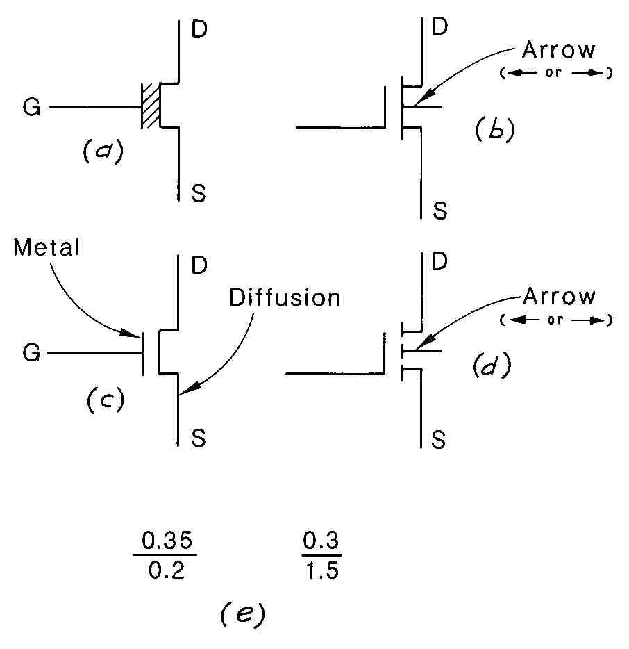
FIG. 14 Symbols used in preceding diagrams: (a) symbol used for depletion
mode MOSFET; (b) standard symbol for the same MOSFET; (C) symbol used
for enhancement-mode MOSFET; (d) standard symbol for this MOSFET; (e)
numbers representing the ratio of the width to length of the source-to-drain
conducting channel.
7. Packaging of Integrated Circuits
Until 1976 or so, two types of package were being used for most ICs: flatpacks and dual-in-line packages (DIPs), ceramic or plastic, although the transistor TO “can” provide a third alternative. Growing pin counts have been forcing some changes, particularly in LSIs and VLSIs. It has become necessary to find the right package for both the system and the chip.
One 3.20-in.- (81-mm-) long DIP has 64 pins. (The one in FIG. 16 is slightly smaller.) The DIP is reliable and easy to position on circuit boards. Since 3-in, bodies take up a lot of board space, however, some designers have turned to more economically sized packages. A redesigned square flatpack with an equal number of leads on all four sides (up to 64 or 80 total) has been gaining acceptance. Multilayered DIPs have been in production, including one that has four rows of pins and is called a QUIP (quadri-chip).
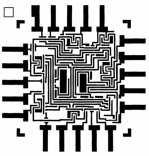
FIG. 15 The pattern for contact metallization (interconnections) of
an integrated circuit. (Bell Telephone Laboratories, now part of AT&T
Technologies.)
A large number of ICs now are available in several packages. One example is the Motorola MC 68000, which can be obtained in a plastic DIP, ceramic DIP, or square chip carrier (see Figs. in earlier section).
Another approach is to use a film carrier, usually for several LSI units. The carrier, which is available in different shapes and sizes, is a multilayer package on the bottom of which is a pattern of “bumps” on 40- or 50-mil centers. There is a metal frame and base pad, making it possible to connect the internal IC pad to the external bumps through grooves in the sides. Another type of carrier uses film, including 35-mm film, which is quite compatible with the automation process. FIG. 17 shows a chip carrier at a and the cross section of a solder bump at b. Small copper spheres are placed on the contact points of the circuit while it is still on the wafer. The wafer is then heated until solder melts over the spheres and forms a solder-coated bump on the contact pad as shown in FIG. 17b. When an individual IC is placed in a header and the assembly is heated, the IC becomes connected to the header through the bumps. Some variations of this appear in FIG. 18, where devices with 50-mil (1.27-mm) distances between leads can be placed on a board with the common 100-mil (2.54-mm) PC-board hole spacing. Thus LSI chips with leads only 50 mils apart can be through-connected to boards that have holes 100 mils apart (see FIG. 19).
MICROELECTRONICS
8. Film (Hybrid) Circuits
A hybrid microcircuit is usually a mixture of etched or silk-screened circuit elements and individual (discrete) elements or standard IC chips. Manufacturing tolerances of resistors and capacitors are smaller in film techniques than in the diffusion process. Therefore, hybrid circuits combining silicon chips that have active devices (transistors and diodes) with film circuits composed of passive devices (resistors and capacitors), are sometimes the most appropriate design for a particular purpose. Hybridization may also minimize weight, space, and interconnections, as well as provide a larger range of values for some elements (see Table 2).
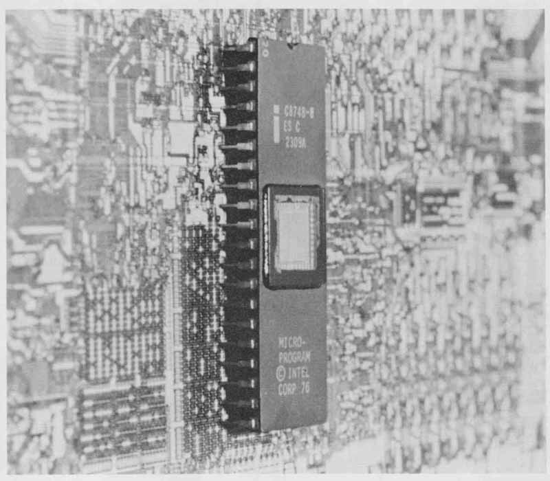
FIG. 16 The 8748 microprocessor package. This 40-pin dual-in-line package
is 3 in. (76 mm) long and 0.6 in. (15 mm) wide. (Intel Corporation.)
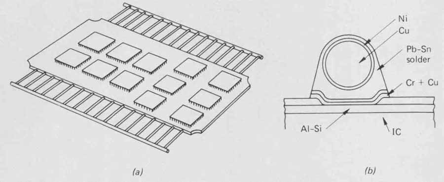
FIG. 17 A chip carrier and solder bump: (a) sketch of a board used
for holding and assembling several chips; (b) greatly enlarged section
of a solder bump.
FIG. 20 shows the same circuit manufactured as a thick-film device and as a thin-film device. Thick-film circuits are made by firing a paste onto an insulating substrate of a glossy or ceramic material. Formerly, expensive noble metals were used, but alloys of lithium, nickel, and copper have recently been used successfully. The deposited material can be from (0.0127) to 2 mils (0.05 mm) in thickness. They are trimmed to the desired accuracy (0.5 to 2 percent) with lasers.
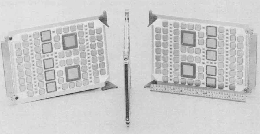
FIG. 18 A ceramic board populated by chip carriers and chip capacitors.
“Front,” edge, and “rear” views. Chip capacitors are the smaller rectangular
shapes that are on the third vertical row “in” from each end, and also
near the center of the board. The largest devices are ceramic multilayer
chip carriers. (Texas Instruments, Inc.)
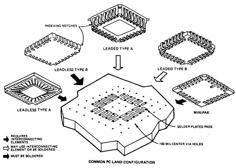
FIG. 19 Packaging for devices with leads or “bumps” at 50-mu (1.27-mm)
centers. Such chip carriers can interconnect with standard circuit boards
having 100-mu (2.54-mm) spacing. (Reprinted from Electronics, March 17,
1977; Copyright © 1977 by McGraw-Hill, Inc.)
Two thin, parallel, light gray lines can barely be seen at the right of each dark resistor area in the upper photograph, where trimming has been performed. (The trimming has been done in the dark areas but does not show up in the photograph.)
Thin-film circuits are different in that the resistor and conductive films are sputtered or vacuum-deposited onto the substrate. The film can be deposited as a pattern or as a film for subsequent photo-processing and etching. Film thickness is a few micrometers, one micrometer being equal to 0.001 mm. Elements are trimmed to the desired size by such processes as abrasive trimming. As in thick-film technology, thin-film techniques are used to manufacture resistors, capacitors, and conductors. They have better resistor stability, resolution, and circuit-element density than do thick-film circuits. However, they are more expensive and cannot produce as large resistance values (see Table 2).
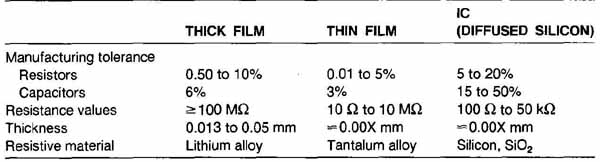
TABLE 2 Data on Film and Diffused Circuit Elements
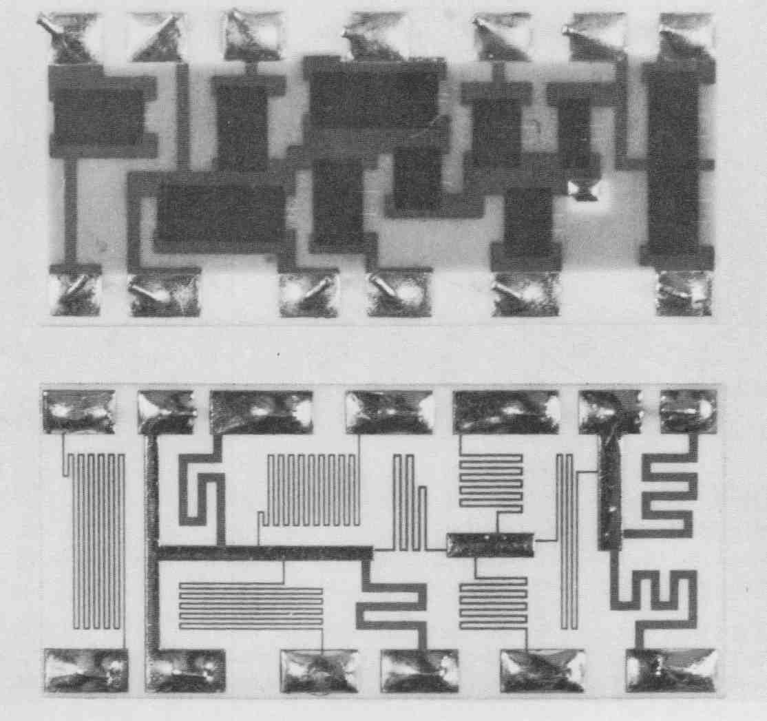
FIG. 20 Photographs of a thick-film circuit (top) and thin-film circuit
(below). These devices, each about 1 in. (25 mm) in length, are the same
as the circuit shown in Fig. 21a.
FIG. 21 shows a schematic diagram of the resistor network that appears in the photograph ( FIG. 20). The lower drawing (FIG. 21b, which is referred to in a later drawing) shows the outline of the substrate and its edge tolerances. FIG. 22 includes the plan view of the thick-film circuit, a table, and some notes. The drawing shows the contacts along the top and bottom and the resistor and conductor areas as hidden lines. A coating to protect against unwanted contact with foreign objects is placed over the resistors and is shown by solid lines which outline its perimeter. A table is included that gives the desired resistance value, resistivity in ohms per square, and desired tolerances. The resistor sheet resistances range from 1 to 100 k per square depending on the film thickness. Tolerances are given in two categories, end of life (EOL) and initial trim. Thick-film resistances have a tendency to drift after they are put into use; hence there are two maximum allowable tolerances, the smaller of which is for the initial trim. Over the life of the circuit (perhaps 20 years), the values are expected to change no more than percentages listed. This drawing was drawn 10 times actual size.
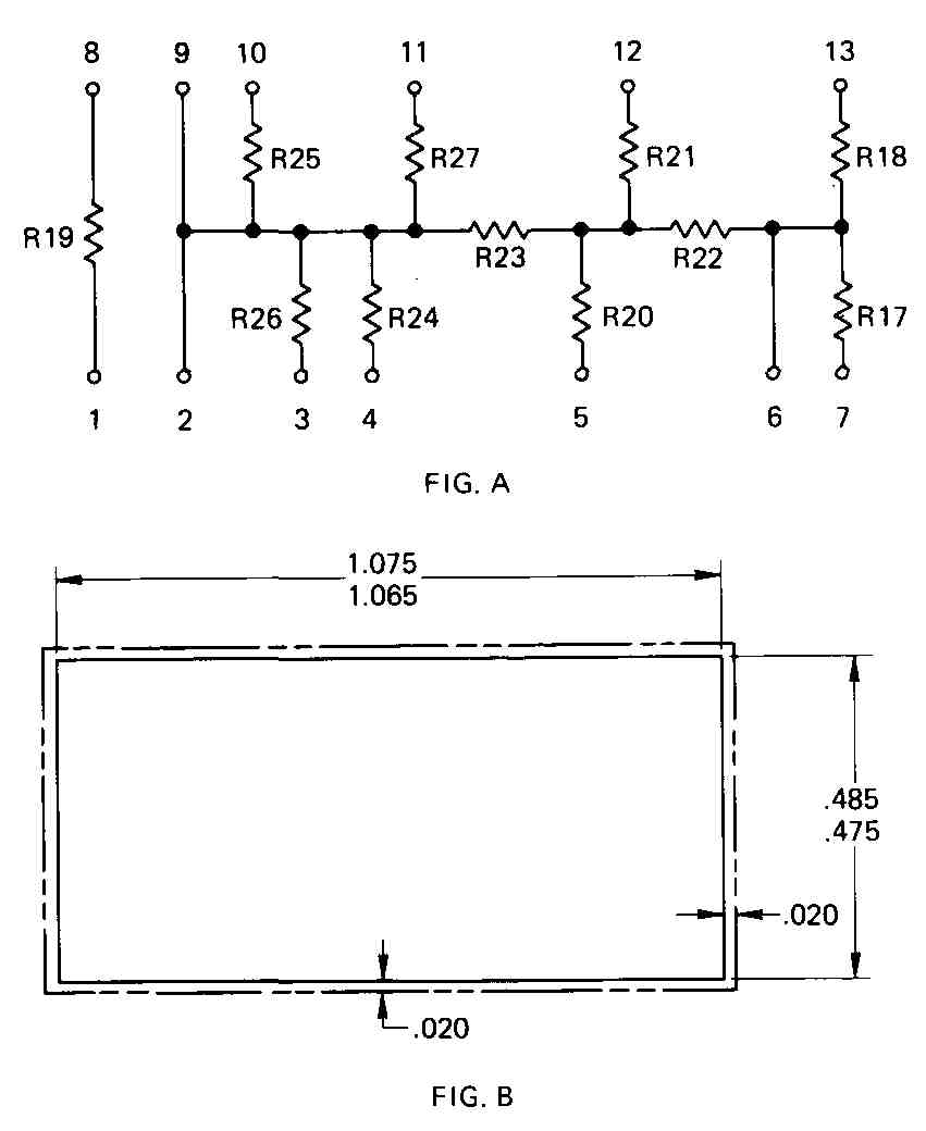
FIG. 21 (a) Schematic diagram of a circuit that has been produced in
both thick- and thin-film form. (b) Outline drawing of the substrate.
FIG. 23 includes the plan view of the thin-film circuit, drawn 10 times desired actual size, notes, and a table. If the resistors have a sheet resistance of, say, 75 per square, the length of a resistor can be determined by an equation such as L = (R/75)(W). Resistor R with a width of 0.0 15 in. (0.38 mm), would have a length of(2000/75)(0.015) = 0.40 in. (10 mm). The designer has to select a route that will provide a 0.015-in.- (0.38-mm-) wide line that is 0.40 in. (10 mm) long. This has been done for each of the resistors in FIG. 21a and results in the patterns that are seen in the drawing and photograph. Note that the higher-value resistors have the narrower lines, 4 mils (0.1 mm). Line spacing has been kept equal to line width. In order to obtain accurate drawings and production models of the circuit, lines of this size are usually drawn by a computer or automatic drafting machine. Notes 3 and 4 of the drawing refer to FIG. 21.
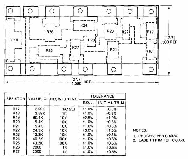
FIG. 22 Working drawing for a thick-film circuit. The schematic of
this circuit is shown in FIG. 21.
Hybrid circuits having different combinations of manufacturing technologies are in extensive use. The hybrid laser preamplifier ( FIG. 24) is a combination of thick-film resistors, thin-film capacitors, and IC chip and chip capacitors on a thick-film substrate. The small black rectangular objects are thick-film resistors, and the four (larger) gray rectangles are thin-film capacitors.
FIG. 25 shows a power MOSFET with vertical integration through different manufacturing technologies. It is a power transistor with additional circuitry with which it will be more versatile and hence more useful. Another device, called SMART Power TM combines what the manufacturer calls CMOS logic and TMOS technology. It is an overvoltage and temperature-protection circuit that can replace three resistors, an SCR, and an integrated circuit ( FIG. 26).