AMAZON multi-meters discounts AMAZON oscilloscope discounts
After studying this Section you will be able to:
- Use symbols in schematic circuits.
- List the qualities of a good schematic and draw a schematic.
- Work from an engineering sketch.
- Reference a component on a schematic.
- Draw a logic diagram and interpret logic symbols.
- Know the function of AND, OR, NAND, NOR, and INVERTER gates.
In this Section you will be studying two similar drawings: schematic and logic diagrams. These drawings usually come after the preliminary drawings, the block and single line diagram.
SCHEMATIC DIAGRAMS
The schematic drawing is a symbolic representation of the data and components used in an electronic circuit. You will learn how the schematic uses symbols from the electronic language. Service, sales, manufacturing, and engineering people can not adequately communicate about an electronics device without the help of a schematic or logic drawing. The way the components are connected will inform the reader of their function. The function will be further explained when you add values, ratings, tolerances, and catalog numbers to the components, FIG. 1.
Engineers and drafting supervisors give you sketches of the schematic from which to work. The sketches given to you as a beginning drafter will be formally laid out. Then as your skills and knowledge increase, the sketches will be only rough layouts of the circuit, FIG. 2. A schematic drawing can be laid out in many ways. No two drafters will organize the drawing exactly the same way. However, they should follow some basic principles. These principles will be discussed later in this Section.
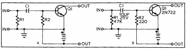
FIG. 1. A—Schematic of a transistor amplifier circuit. B—Add more information
chiefly to help a technician troubleshoot the circuit.
FIG. 2. A—Formal engineering input to the drafter. B—An engineering
input submitted as a rough sketch.
DRAFTING SCHEMATICS
When drafting a schematic, your responsibilities are:
1. To organize the schematic to fit a specified paperformat. Often schematics must fit into books. This requires you to draft your drawings to a size that will fit the book or can be reduced appropriately to fit the book.
2. To apply proper symbols and reference data for each component. This will be accomplished by having an understanding of American National Standard Institute’s (ANSI) Y32. 1 6 Reference Designations for Electrical and Electronics, Y32.2 Graphic Symbols for Electrical and Electronics Diagrams, and Y32.14 Logic Diagrams, Graphic Symbols (AIEE/IEEE91).
3. To create general notes, legends, or detailed notes that explain specifics of the schematic.
4. To follow the general rules when drafting the schematic.
RULES FOR DRAFTING SCHEMATICS
All drawings have general rules for the way they are created. The schematic should be drawn using the following rules:
1. Normal signal flow should be from left to right, top to bottom. An example would be a radio circuit, FIG. 3. The antenna (input) should be on the upper left of the paper. The speaker (out put) should be on the right side.
2. Lines should be spaced a minimum of 3/8 in. (10 mm) apart.
3. Lettering should be 5/32 in. (4 mm) high. This requirement is necessary for microfilming and
photo-reductions of the drawings.
4. Lines between components should take the shortest path.
5. Connecting lines should have a minimum of crossovers and joggles, FIG. 4 A and B.
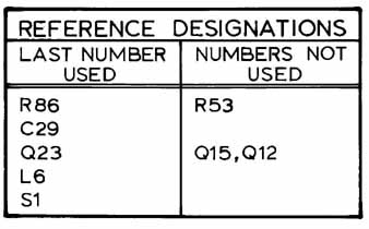
6. Long parallel lines should be arranged in groups, preferably three to a group, FIG. 4 B and C.
7. Avoid four-way tie points or four-way junctions, FIG. 5.
8. Power sources should go up and ground lines should go down, as shown in FIG. 6.
9. All lines will run horizontally or vertically and connect in 90-degree corners, FIG. 7. A flip-flop or crossover circuit is the only exception to this rule.
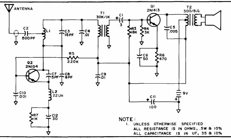
FIG. 3. A schematic showing left to right signal flow. Signal travels
from the antenna to the speaker on the right.
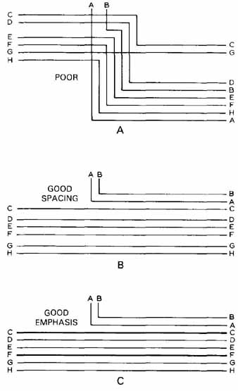
FIG. 4. An example of how to handle jogged, crossover, and parallel
lines. A—The eye cannot easily follow a line. B—Regrouping and periodic
spacing helps. C—Periodic thick lines are one common method of improving
readability.
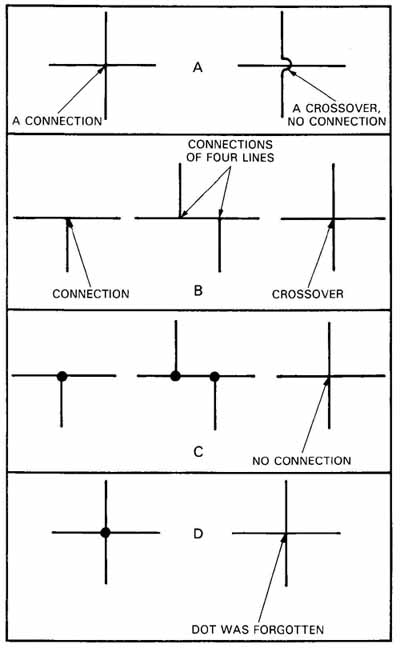
FIG. 5. Junctions and crossover methods used on schematics. A—An outdated
method. B—Method without dot makes only one junction at a given place.
C—Method using single junction with dot is most preferred. It helps trip
reader’s eye when it scans a line. D—Avoid four-way tie points in case
you forget the dot.
FIG. 6. A—An example of power sources up and ground lines down. Some
engineers prefer the heavy bus lines for the ground and power ties. B—When
many lines will be crossed, use a common ground symbol and power symbol.
Note: The + 5V of the bottom circuit does not go to the top of the paper.
It simply goes up. This saves crossing lines and makes the drawing easier
to read.
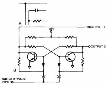
FIG. 7. A—An example of normal lines. All are drawn horizontally or
vertically with connections made at right angles. B—A flip-flop circuit
is an exception. It uses diagonal lines to show the crossover function.
REFERENCE DESIGNATIONS
Reference designations are combinations of letters and numbers. FIG. 8. They are used to identify components shown on the schematic. The reference designation should be located as close to the graphic symbol as possible.
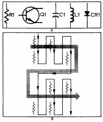
FIG. 8. A—An example of components and their reference designations.
B—How to number the components in the proper order.
Numbering of components should be in a sequential order starting from upper left and proceeding left to right, top to bottom. When items are eliminated because of drawing revisions, the remaining items are not renumbered. But you create a table to show the missing or sometimes forgot ten numbers, FIG. 9.
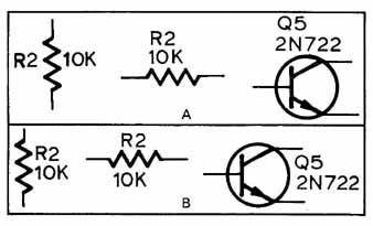
Placement of references will be dictated by each company’s drafting standard. Most companies will follow the methods shown in FIG. 10. To save room on a crowded schematic, some companies prefer the metho1. When the schematic is crowded, and lines must be spaced a minimum distance apart, method (B) is the preferred way of referencing the components.
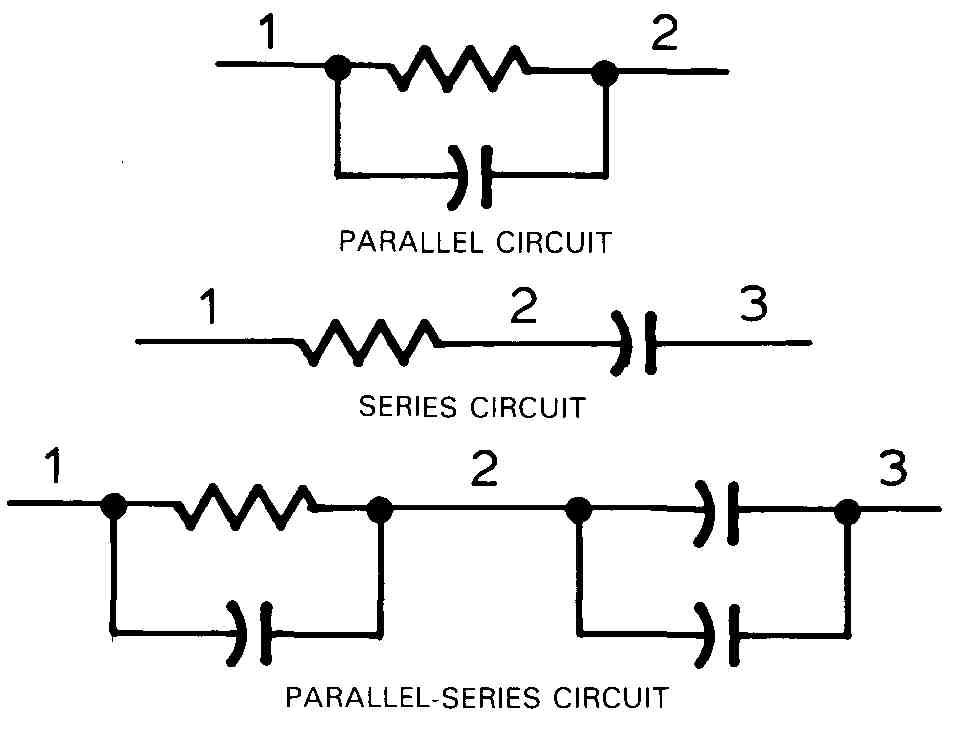
FIG. 12. Series and parallel circuits. The potential will change at
each junction. Note the numbers on the examples. Each number represents
a new or different potential.
LOGIC DIAGRAMS
Logic drawings are diagrams representing the logical elements and their interconnections. They will most often not show the component’s elements or internal details. They will use symbols and supplementary data to describe the function of each element. Symbols for logic diagrams are covered in Graphic Symbols for Logic Diagrams (two-state devices) ANSI Y32.14.
TYPES OF DIAGRAMS
There are two main types of logic diagrams, a basic and a detailed diagram, FIG. 15. The basic diagram shows logical functions and their relation ships without reference to physical relationships. It uses logic symbols to show the main concept of the circuit. Detailed diagrams take the basic information and add specifics or non-logic data. This data may include pin numbers, test points, and other necessary physical elements.
LOGIC ELEMENTS
There are a few elements used in logic diagrams. They are: AND, NAND, OR, NOR, and INVERTER GATES, plus Operational Amplifiers, Flip-Flops, Schmitt triggers, Decoders, Counters, Shift registers, and Oscillators. These are some of the most frequently used elements.
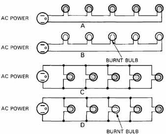
FIG. 13. Effect of series circuit and parallel circuit. A— Lamps in
series. B—String of lamps are all out when in series circuit. C—Lamps
in parallel. D—String of lamps are on except for burnt bulb in parallel
circuit.
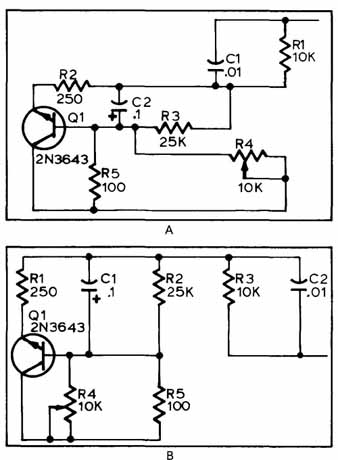
FIG. 14. A parallel-series circuit shown before, A, and after the drafter
rearranged it. Example B lines the components up so the lettering can
be done on a common line, making the circuit easier to read.
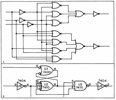
FIG. 15. The two most frequently used logic diagrams. A—Basic logic
diagram. B—Detail logic diagram.
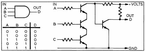
FIG. 16. An AND gate symbol, its schematic, and truth table.
LOGIC TERMS
AND gate—A gate circuit with more than one in put terminal, FIG. 16. No output signal will be produced unless a pulse is applied to all inputs simultaneously. In binary circuits all inputs must be “1”to get an output “1 “. If any of the inputs are zero, the output will be zero.
INVERTER gate—A circuit that takes a positive signal input and puts out a negative signal, or vice versa, FIG. 17. It has one input and one output. It is often called a NOT circuit since it produces the reverse of the input.
NAND gates—A combination of a NOT and AND function, FIG. 18. It has two or more inputs and one output. The output is logic “0” if all the inputs are “1 “. If any input goes to “0” the output goes to “1 “. With logic of the opposite polarity, this type gate becomes a NOR gate.
OR gate—The OR circuit performs the function of producing an output whenever any one (or more) of its inputs is energized, FIG. 19.
NOR gate—A combination of an OR and NOT function, FIG. 20. It will have an output of “0” if any input is logic “1” and is logic “1” only if all the inputs are logic “0”. With an opposite logic polarity, this gate can become a NAND gate.
Operational Amplifier (Op Amp)—An amplifier that performs various mathematical operations. They can be used to add, subtract, average, integrate, and differentiate. It may have a single in put and output, FIG. 21.
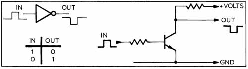
FIG. 17. An INVERTER (NOT) symbol, its schematic, and truth table.
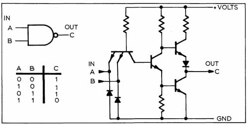
FIG. 18. A NAND gate, its schematic, and truth table.
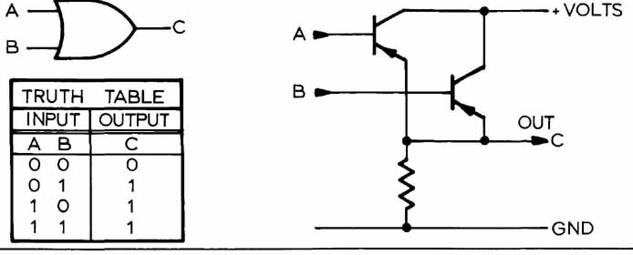
FIG. 19. An OR gate with schematic and truth table.
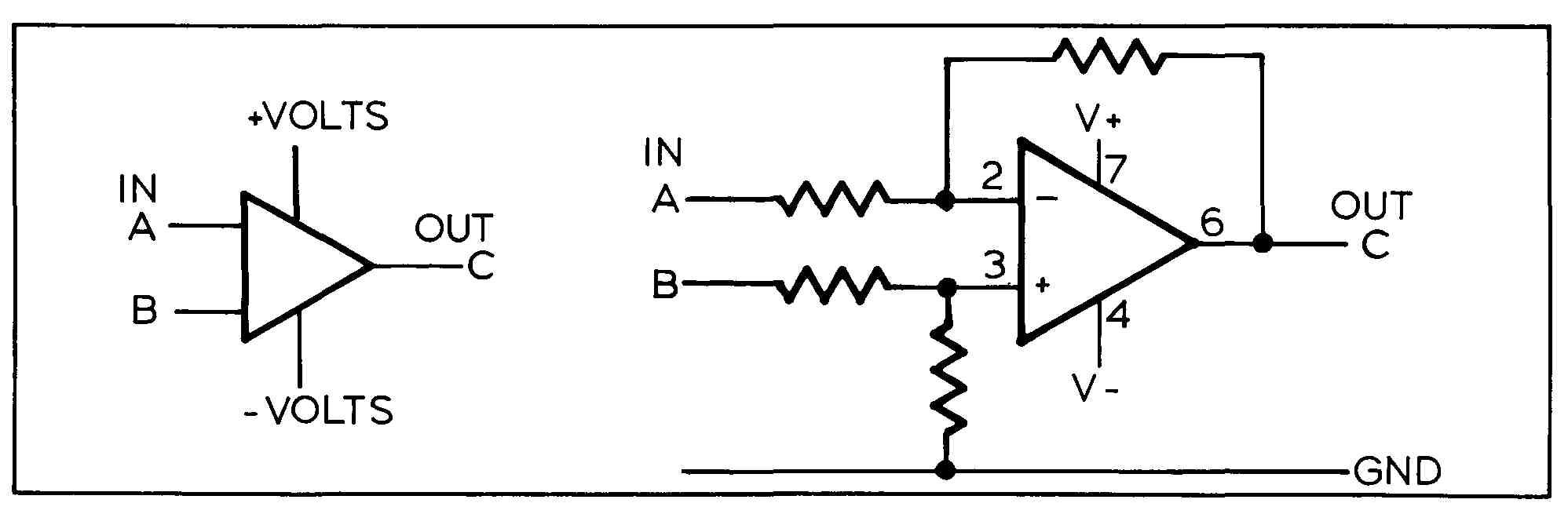
FIG. 21. A two input Operational Amplifier (Op Amp) with external resistors
added to the symbol.
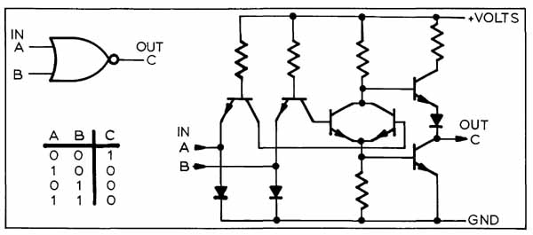
FIG. 20. A NOR symbol, its schematic, and truth table.
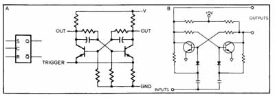
FIG. 22. A—Flip-flop symbol and a schematic of the flip-flop function.
B—Another type of flip-flop.
Flip-Flop—A flip-flop, FIG. 22, is a device which is stable in either of two states. When triggered by an input or clock pulse, the flip-flop moves from one stable state to the other. For example, if one of its outputs, called Q, starts at 1, it will be at 0 after the input pulse.
The most common flip-flop is the JK type. Another type is the set-reset (RS) flip-flop. Some types require both an input pulse and an “enable” pulse.
Schmitt Trigger—A bistable pulse generator in which an output pulse of constant level exists only as long as the input is constant, FIG. 23.
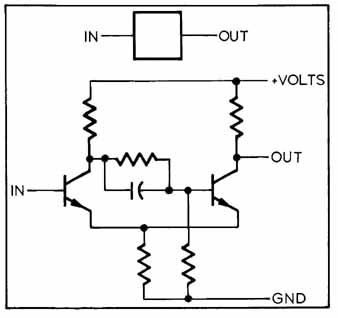
Fig. 23
Decoder—A device for translating a combination of signals into one signal. It is often used to extract information from a complex signal or coded signal, FIG. 24.
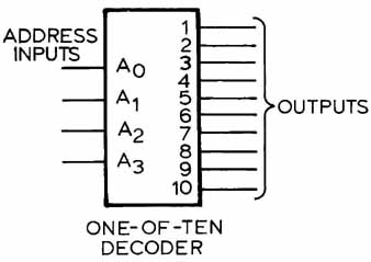
FIG. 24. A decoder with four inputs and ten outputs.
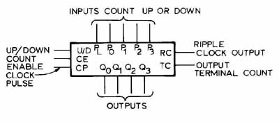
FIG. 25. A counter circuit symbol. The device can count up or down
Counter—A logic device that counts input pulses, FIG. 25. It may count
input pulses and then out put after a predetermined number has been received.
The counter may count up or down. Shift register—A circuit which can
shift information from one flip-flop in a chain to an adjacent flip-
flop when it receives a clock pulse, FIG. 26.
Oscillator—An electronic device that generates alternating current of predetermined frequencies,
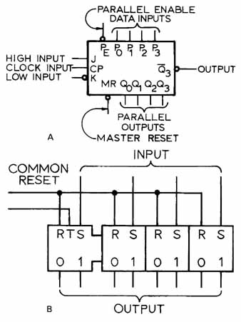
FIG. 26. A—Shift register symbol. The unit is used for data transfer.
B—Four flip-flops used as a four-stage shift register.
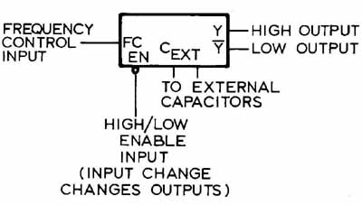
FIG. 27. The oscillator circuit is designed to take a voltage impulse
and produce a current that periodically reverses. To properly draw oscillators
and other elements correctly in the logic diagram, you must follow some
basic rules.
Rules for drawing logic diagrams
1. Draw each device so that the input is on the left or top of the element.
2. Outputs of logic elements should go to the right or down.
3. The basic rules for schematics apply also to logic diagrams.
4. The numbering of logic elements will be by physical positions in the equipment. This rule will differ from the schematic which is numbered left to right and top to bottom disregarding physical position.
REVIEW QUESTIONS
1. Long parallel lines should be put in groups of _____ (how many).
2. List the drafter’s responsibility when drawing a schematic.
3. Which way should the schematic’s signal flow?
4. Why should we avoid four-way tie points?
5. What are reference designations?
6. In what symbol can diagonal wiring lines be used?
a. AND
b. Op Amp.
c. NOR
d. Flip-flop.
7. What is a parallel circuit? Sketch one.
8. What is the standard source for symbols for logic diagrams?
9. What are the two main types of logic diagrams?
10. List the basic logic elements.
PROBLEMS
PROB. 1. Draw a formal schematic of the panel- mounted components for the AM-FM radio shown in FIG. 28. Draw on “A” size vellum. Add reference designations and make appropriate changes to the symbols.
PROB. 2. Prepare a schematic of the AM transmitter shown in FIG. 2 9. Sketch the circuit layout before going to the final drawing.
PROB. 3. Draw a schematic of the transistor amplifier shown in FIG. 30. Add correct reference designations for all components.
FIG. 27. The frequency control of an oscillator sets its frequency.
PROB. 4. Create a formal schematic of the push- pull amplifier, shown in FIG. 31.
PROB. 5. Draw a schematic of the oscillator circuit shown in FIG. 32. PROB. 6. Create a logic drawing of the partial circuit shown in FIG. 33.
PROB. 7. On an “A” size sheet, make a drawing of the logic circuit shown in FIG. 34.
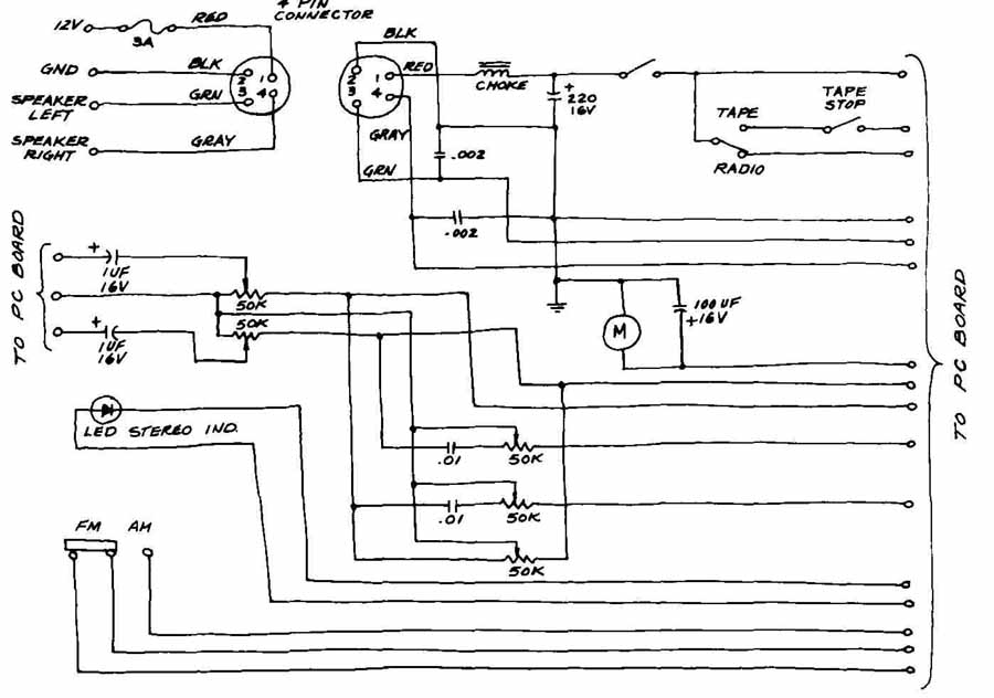
FIG. 28. Draw a schematic of an AM-FM radio’s panel-mounted components.
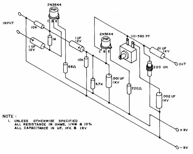
FIG. 29. Draw a schematic of an AM transmitter circuit.
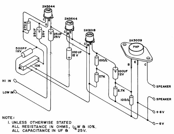
FIG. 30. Draw a schematic of transistor amplifier.
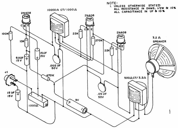
FIG. 31. Draw a push-pull amplifier schematic.
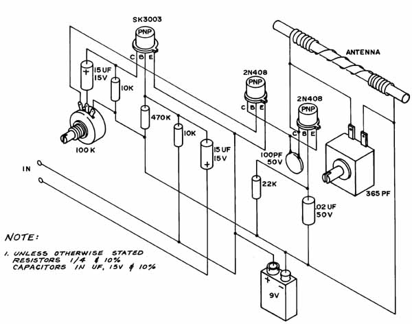
FIG. 32. Draw an oscillator circuit.
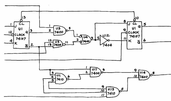
FIG. 33. Redraw a portion of a logic circuit.
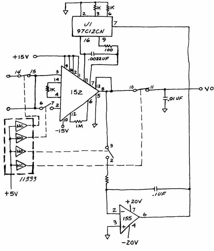
FIG. 34. Redraw a logic circuit having a variety of Op Amps and output
modules.