AMAZON multi-meters discounts AMAZON oscilloscope discounts
After studying this Section, you will be able to:
- Lay out a printed circuit board.
- Create a drill and trim drawing.
- Tape a printed circuit artwork.
- Create a printed circuit board assembly drawing.
- Explain a process for etching printed circuit boards.
The drafter will begin creating the printed circuit board (PCB) after receiving a schematic or logic drawing and a list of components. The engineer will provide this information and any other necessary design data.
SCHEMATIC OR LOGIC DIAGRAMS
These drawings will show the functions and major circuit paths of the electronics circuit. See FIG. 1. The schematic shows the power and signal paths for individual components. The logic drawing shows the data paths for digital or analog circuitry. The first step in PCB layout and design is to study the engineering input.
DESIGN DATA
The engineer will provide the following design information:
1. The voltage and amperage ratings of the circuit.
2. Heat-sink requirements for heat-dissipating components.
3. Grounding requirements.
4. Board size and mounting technique.
Numbers 1, 3, and 4 of these design requirements will be discussed later in this Section.
ADVANTAGES OF PRINTED CIRCUITS
Printed circuitry has some distinct advantages over other methods of interconnecting circuits. The major advantages are:
1. They can be automatically assembled and soldered.
2. Their consistent quality reduces inspection time.
3. They have a lower production cost. This is true only when many of the same boards are required.
4. They can reduce size and weight.
5. The circuit capacitance will not change from circuit to circuit as in wiring techniques.
6. Their plug-in capability makes them easier to service.
The above advantages make printed circuits the heart of most electronic devices.
PCB LAYOUT
To start the layout we need to gather all the necessary component, circuit, and board information. The engineer will provide ratings (volts, amps), but you must gather much of your own component information. The necessary component information will be: the size of the component, how it is mounted on the board, and what size mounting holes are required, FIG. 2. With the gathered in formation, you can now start to work on the PCB.
DESIGN SCALE
The most common scales used to create Printed Circuit Artworks are 1X, 2X, and 4X. All complex circuitry should be prepared at an enlarged scale Drafting errors such as poor placement of mounting pads, conductor spacing, and other errors will be reduced by the multiplier when photographed to give a 1 to 1 scale. Precision layout grids, manufactured component patterns, numerically controlled hole drilling, and automatic component insertion dictate the artwork scale. NC drilling and automatic stuffing should be at .025 in. intervals. Therefore, the precision grids are . 1 0 or .05 and the component patterns are designed around that interval.
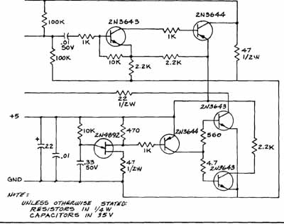
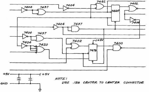
FIG. 1. A—The schematic interconnection information. Component information
is included for size consideration. B—The same information on a logic
drawing.
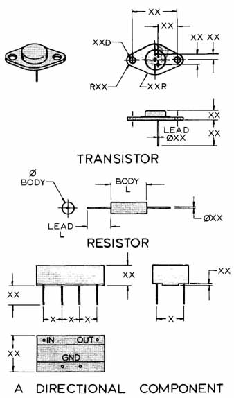
FIG. 2. This is an example of the information you will find in a components
catalog. This data is vital to the completed design layout.
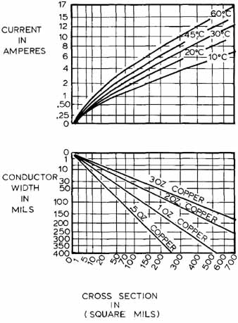
FIG. 3. A graph used to decide how wide the conductor should be. Note
the width is determined by the amperage causing heat in the circuit.
Artwork with a 1 to 1 scale is used only when you need a quick prototype board, or limited accuracy is required.
CONDUCTORS
Care must be taken in deciding width and spacing of conductors. Conductor widths or cross sectional area is determined by current carrying requirements. FIG. 3 shows the ratio of amperes to the cross sectional area of the conductor.
Spacing of conductors is dictated by the amount of voltage in the circuit, the altitude when used, and the board’s coating. When the board is used at higher altitudes as in an aircraft, you are required
to increase the voltage gap. The lower barometric pressure at higher elevations will allow the current to arc across the voltage gap easier. Coating the board with an insulation helps prevent voltage arcing. See FIG. 4 for spacing requirements.
BOARD SIZE AND STYLE
The simplest board to manufacture is a single layer board, FIG. 5. This board will have circuitry only on one side. The opposite side will be the component side. Single layer boards are the least ex pensive to manufacture. However, they will not meet all requirements. High density boards require more layers. They require the use of double-sided or multilayer boards.
Double-sided boards allow you to apply circuitry to both sides of the board, see FIG. 6. With this method, you will try to apply the maximum amount of circuitry on the circuit side. Having less circuitry on the component side will reduce the problem of having components over the circuitry. In extremely dense circuitry, you may use multilayer boards. Multilayer boards with as many as 20 layers have been used. See FIG. 7.
FIG. 4. [coming soon] This table shows how voltage, elevation, and an insulation coating can determine the spacing of conductors.
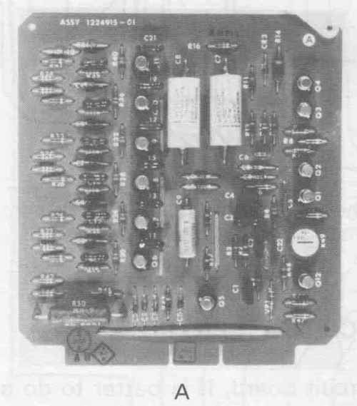
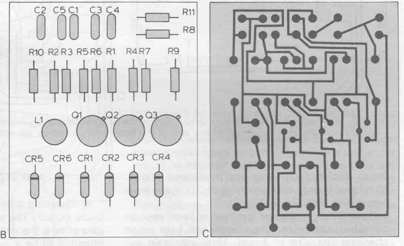
FIG. 5. A—Single-sided board. It is the least expensive and simplest
to manufacture. B—Marking artwork, single-sided board. C—Circuit side
of board in B.
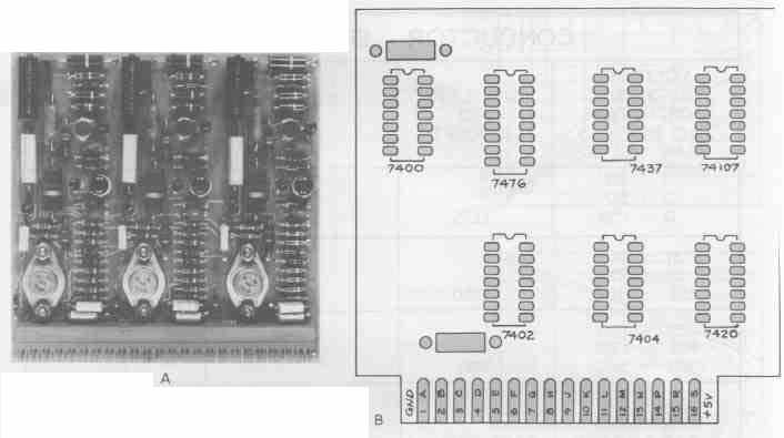
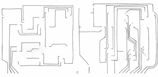
FIG. 6. A—Double-sided board. Note the circuitry on the component side.
B—Another double-sided board. C—The conductors normally flow horizontal
on one side of the board and vertical on the other. Sketches refer to
board in B.
Once the style of board has been chosen, you can consider board size. Experience will help when choosing the size of board. Until you gain experience, you may need to look at previously manufactured boards for a guide.
A SKETCH FOR A LAYOUT
In designing a circuit board, it is better to do a quick sketch. The sketch will allow you to get an idea of how the circuit will flow. This sketch is not intended to be a work of art. It only needs to be organized enough so that another drafter can work from it if required, FIG. 8.
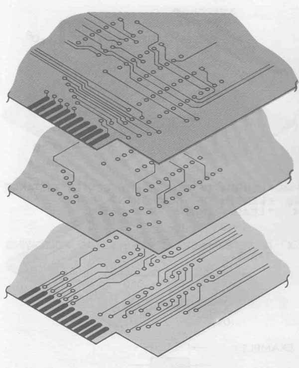
FIG. 7. The levels of a multilayer board. Boards have been manufactured
with up to 20 layers.
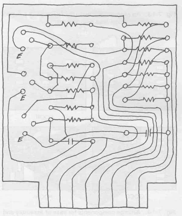
FIG. 8. A sketch of the PCB used to decide on component placement and
how the interconnections will flow.
PREPARE FORMAL LAYOUT
After you achieve a workable sketch, you are ready to go to a more formal layout. This layout will be accomplished with templates or PUPPETS.
With templates, you can draw the scaled component outlines on the layout. See FIG. 9.
Puppets are pre-made component outlines which are put on an adhesive backed format. They can be adhered wherever you wish on the layout.
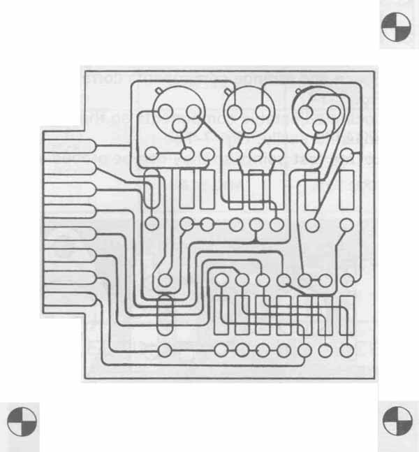
FIG. 9. A formal layout with each component shown true size and with
all interconnections figured for taping.
This formal layout should be drawn on a gridded format. The first step will be to lay out the edges of the board, including any connectors. Second, you should apply DATUM TARGETS, FIG. 9. These targets will be used as exact points for measuring purposes. Three targets are normally applied. If more than one sheet will be used in the layout, each sheet should have targets. The targets will allow you to re-register the layers each time they are mated together. These targets will also be used for photographing the artwork and during board manufacturing. Photographic targets or reduction points may also be used to help in the etching process. Etching is the chemical removal of the cop per on the circuit board. FIG. 10 shows how these points serve in the etching process when placed on the PCB.

FIG. 10. A target being used for checking the etching process. A—A
good etch. B—Needs more material etched away. C—Over-etched.
After you have finished the above tasks, you can continue with the following:
1. Represent the physical shape of each component on the layout, FIG. 11.
2. Indicate the polarity of polarized components, FIG. 12.
3. Establish the mounting requirements for each component, FIG. 13.
4. Space and arrange components correctly. See FIG. 14.
5. Locate adjustable components so they can be adjusted easily, FIG. 1 5.
6. Locate test points so they can be probed with the unit operating, FIG. 16.
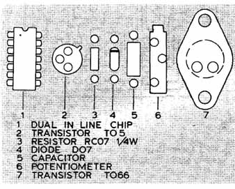
FIG. 11. An example of how components would be represented on a layout
drawing for a PCB. The drafter will determine circuit path locations
from terminals.
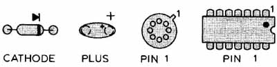
FIG. 12. Indicate polarity on components that can be plugged in incorrectly.
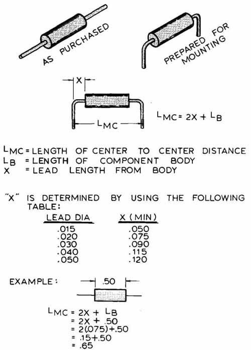
FIG. 13. An example of how to figure mount spacing on axial lead components.
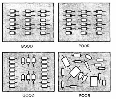
FIG. 14. Arrange components for ease of assembly and inspection. Note
how much longer it would take to inspect correct installation of the
poor arrangements.
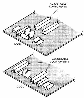
FIG. 15. Place adjustable components so the adjusting tool can easily
reach them.
7. Place all mounting pads if possible on grid line crossings, FIG. 17.
8. Indicate size of holes required to mount components, FIG. 18.
9. Select terminal size required to solder component to PCB, FIG. 19.
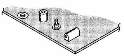
FIG. 16. Locate all test points so that measurements can easily be
made with equipment in operation.
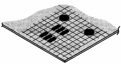
FIG. 17. The placement of pads on grid crossing. This is done to aid
automated drilling and component assembly.
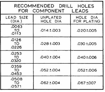
FIG. 18. A table of recommended hole sizes for different component
lead diameters.
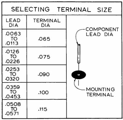
FIG. 19. A table showing the mounting pad diameter for the different
lead diameters. This is to insure an adequate solder area around each
terminal.
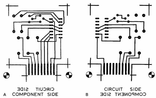
FIG. 20. A—The blue tape side on a single format artwork. B—The format
is flipped over showing the red tape side of the circuit.
PRINTED CIRCUIT ARTWORK
Artwork can be created in different ways. There are two basic methods used in most companies. One method uses red and blue tape on a single sheet of plastic format. The second method is to use different sheets of format for each board level.
RED AND BLUE ARTWORK
Using the red and blue method, you can create a double-sided PCB on a single artwork sheet. For the double-sided board, start by placing component mounting pads on a clear film. After placing the pads, continue by taping the blue side (usually the component side). See FIG. 20A. Tape all interconnections on this side, then turn the film over and tape the solder side, which is usually done with red tape, FIG. 20B.
Do not tape both red and blue circuitry on one side of the film. This error will make it difficult to make changes on interconnections underneath other colored tape.
MULTI-SHEET ARTWORKS
Multi-sheet drawings will start with placement of component mounting pads on a single layer of film (the pad-master), FIG. 21 . Then another film will be placed over the pad-master and the component side will be taped. Each additional layer will be placed over the pad-master and taped.
TAPING TECHNIQUES
The taping assignment is a critical job. It is one time when you are not just creating a drawing but also a manufacturing tool. Many times you are required to tape the artwork to ± .005 in. Consider five basic taping rules:
1. Avoid sharp corners, which can cause problems in etching, soldering, and with foil delamination, FIG. 22A.
2. Keep interconnections as short as possible. See FIG. 22B.
3. Keep the tapes and media clean. Any dirt or smudges will show up on the artwork photos.
4. Spread the circuitry out so it is evenly placed throughout the board. If it is concentrated in one area of the board, it will cause localized heating when automatic soldering. This uneven heating will warp the PCB.
5. Make terminals larger than interconnecting lines. This will prevent solder from flowing away from the solder terminal, FIG. 22C and D.
These basic rules will assure quality taped art work. This artwork is then ready to be used as the etching tool.
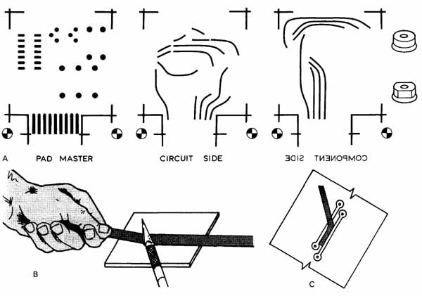
FIG. 21. A—The taping of a multi-sheet artwork. Note registration pins.
B—Overlap tape on pad. Cut by lifting tape against fixed blade to avoid
cutting the taped circuit paths below. C—Space the conductors with temporary
spacing tape.
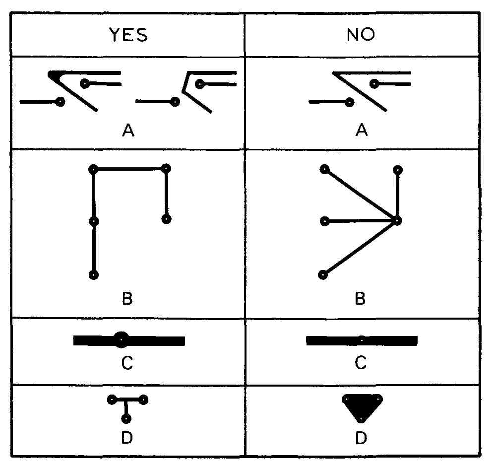
FIG. 22. General taping rules for all PC boards. Some companies add
their own specific requirements.
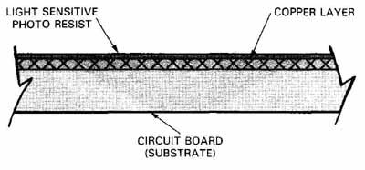
FIG. 23. The basic structure of a PC board.
ETCHING A PCB
Most industrial PC boards are created by using a photographic process. You will study this process to find how your artwork will be used in PC board manufacturing. The steps in manufacturing normally follow this standard sequence:
1. Purchase a PCB, FIG. 23, which is made up of three layers:
a. The board, a flat stiff sheet of insulating material, often called the substrate.
b. Copper foil laminated to the substrate.
c. A photosensitive resist that will harden when exposed to ultraviolet light.
2. Drill holes from the drilling specifications. These specifications will be listed on the drill and trim drawing to be discussed later.
3. Expose the board to ultraviolet light. For this, use an artwork negative to control where the light exposes the board, FIG. 24.
4. Wash away unhardened resist and etch the board. The resist not exposed by the light will quickly wash away, allowing the etching chemicals to eat away the copper underneath. When the etching is finished, you will see the circuit you designed, FIG. 25.
5. Plating the connectors is necessary if they are pluggable edge connectors. The connectors are normally plated with gold because of its corrosion resistance and excellent current carrying ability. See FIG. 26.
6. Tinning is next. It is the coating of the PCB with a tin-lead alloy, FIG. 27. This is done to set the board up for soldering and to decrease the oxidation problem. Copper will oxidize more readily than tin-lead.
7. Trim the board to its specified final size. FIG. 28 shows the result.
8. Inspect the board for flaws. Flaws will be described in each company’s PCB manufacturing specifications book.
ULTRAVIOLET LIGHT SOURCE
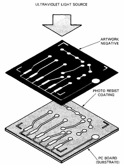
FIG. 24. The PCB is exposed to ultraviolet light. The tight will harden
the photo resist that it illuminates. This will set up the etching process.
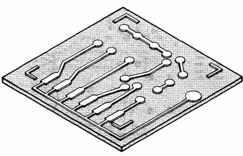
FIG. 25. The PCB after it has been etched by acids.
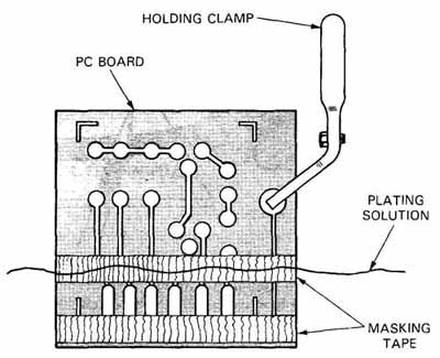
FIG. 26. The PCB has been masked off so the connecting contacts can
be plated with gold.
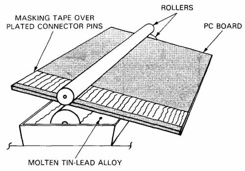
FIG. 27. Tin-lead alloy is being rolled on to the PCB. Note the previously
gold plated connector contacts are covered with masking so they will
not be coated with tin-lead.
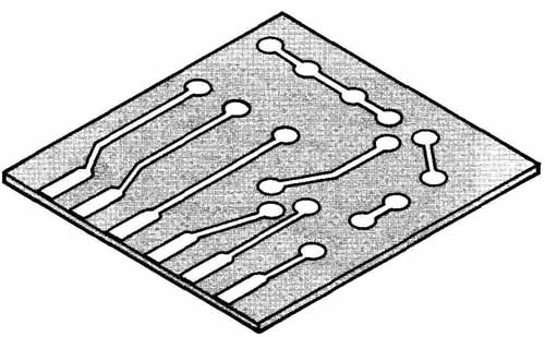
FIG. 28. The final board trimmed to size.
PRINTED CIRCUIT DRAWINGS
There are at least five drawings required to document a PCB. They are: a logic or schematic drawing, a layout, artwork, drill and trim, and assembly with parts list. Optional drawings will be silkscreen drawings of component positions and component reference designations. You will study each of these drawings.
LOGIC OR SCHEMATIC
The schematic shows the circuit interconnections in the most compact way. It will be used to test and evaluate the completed circuit board.
LAYOUT
The layout is a preliminary ink drawing which is used to confirm design ideas for the electronic circuit, FIG. 29. It takes the symbolic schematic or logic drawing and transforms it into a model of the mechanical package. The layout will normally contain all the design information required to produce a PCB. All interconnecting lines, components, component placement, component mounting, board size, and connectors should be considered at this drawing level.
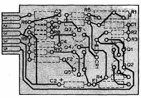
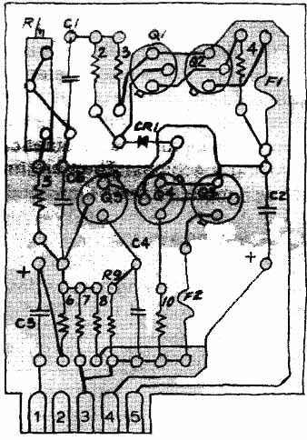
FIG. 29. A layout is an ink drawing meeting the physical requirements
of the circuit.
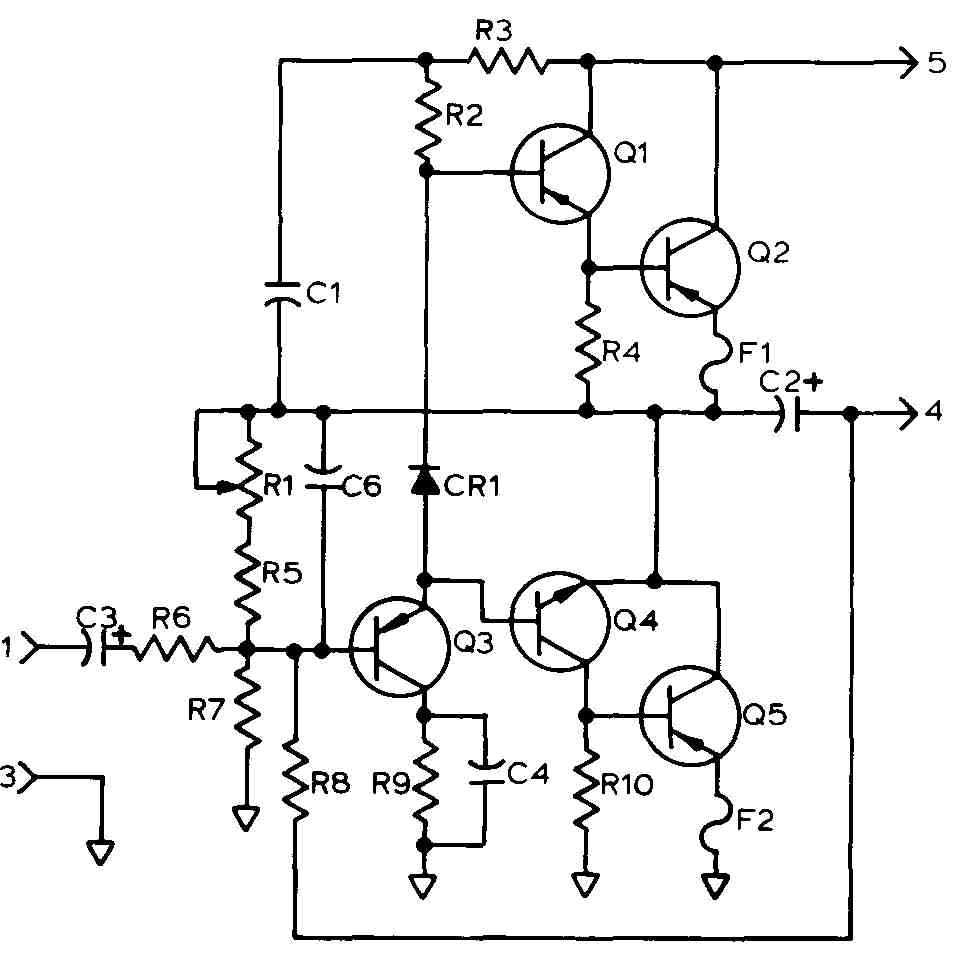
FIG. 30. A sketch as it relates to the schematic. A sketch may be the
only step before the artwork. All interconnections are figured at this
level.
Some PC board designs are created from a sketch, FIG. 30. The sketch may be the only step before the artwork. In other cases, it is just one of the steps before the artwork.
ARTWORK
The artwork is designed to be used as a tool to create the PCB. Because this drawing is used in the fabrication process, it is a critical step, FIG. 31 As the PC boards get smaller and the density gets greater, it is becoming impractical to tape the art work by hand. The circuitry is automatically drawn by laser plotting machines. They are many times faster and much more accurate than hand methods.
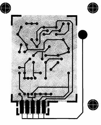
FIG. 31. The artwork for a single-sided circuit board. It is hand-taped.
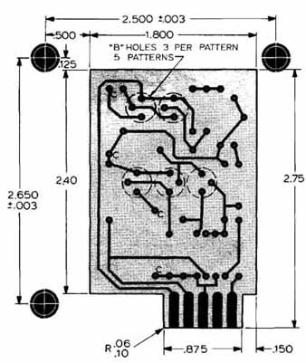
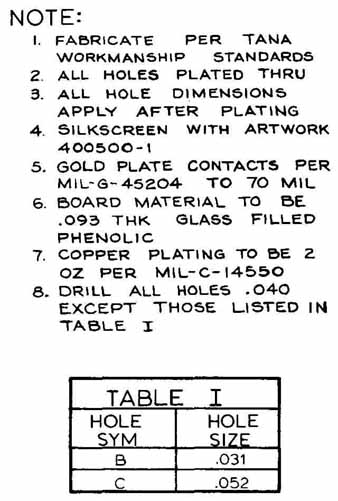
FIG. 32. A drill and trim drawing. It is used to describe all the mechanical
requirements of the PCB.
DRILL AND TRIM DRAWING
The drill and trim drawing totally describes the design and manufacture of the PCB, FIG. 32. It includes the following:
1 . All dimensions needed to cut the outline of the board.
2. All drill hole information:
a. Size of hole.
b. Plated or unplated holes.
3. Description of material:
a. Board material.
b. Copper layer.
c. Gold plating.
4. Photo reduction information.
ASSEMBLY DRAWING
The assembly drawing takes the etched board and adds all components and other assembly items, FIG. 3 3. It will show a view of the component side with all components stuffed. A complete parts list will identify all material and components needed. Notes will be added to clarify any information.
SILKSCREEN DRAWING OPTION
The silkscreen will normally show component reference designations and/or component placement, FIG. 34. This information helps in board assembly, inspection, and service. It is vital when a board is set up to make optional choices. The options can be silkscreened on the board to make changes accurate and timely, FIG. 35.
REVIEW QUESTIONS
1. The logic drawing shows ____ paths for digital or analog circuits.
2. List some advantages of printed circuit boards.
3. Drafting errors are ____ after a drawing is reduced photographically.
a. More obvious.
b. Repairable.
c. a and b.
d. Less obvious.
4. Describe the etching process.
5. What factor does voltage play when you design a PCB?
6. List the information needed before you start a PCB layout.
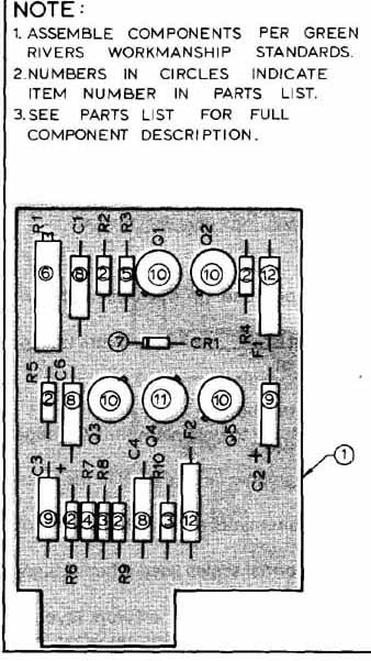
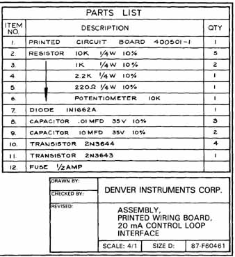
FIG. 33. An assembly drawing with a parts list. The list is used for
parts purchasing and description. The assembly drawing will show manufacturing
how and where to “stuff” each component.
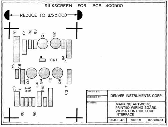
FIG. 34. Silkscreen drawing used to show assemblers quickly where each
component goes and the polarity of each.
Often called marking artwork, it is used to print instructions on the PC board. Note reduction marks.
FIG. 35. An example of how a silkscreen drawing will assist the assemblers
in setting up desired customer’s options. Jumper wires re-route the circuit
as needed. Instructions may be marked on the PCB.
7. What is the purpose of the drill and trim drawing?
8. An inked layout is ______ a PCB artwork taping.
a. The result of.
b. Done before.
c. The only step before.
9. Why is it necessary to gold plate the PCB edge connector pins?
10. How are photographic targets used in the etching process?
11. Amperage requirements affect what aspect of PCB design?
12. What are the normal scales used when designing a PCB?
13. When would you do a 1 to 1 artwork layout?
14. Why do you use a 10th grid format when laying out a PCB?
15. List the information found on an assembly drawing.
FIG. 36. A typical schematic as submitted to drafting by the engineer.
Draw a formal schematic.
PROBLEMS
PROB. 1.
PROB. 2.
PROB. 3.
PROB. 7.
PROB. 8.
Using the BOT-EOT schematic, FIG. 36 and components on FIG. 37, create a formal schematic. Add reference designations to the schematic.
Design a printed circuit board from the BOT-EOT schematic. The board size should be 2.50 x 4.5 in. Inputs and outputs should be on the same side of the board. The connection terminals should be .375 dia. at 2X scale. It should be a double-sided board, so use a red and blue pencil for the layout. Tape the BOT-EOT board into a formal artwork. Tape width should be .05 and the spacing .05. Use a 10th grid to control the taping.
PROB. 4. Create a drill and trim drawing of the BOT-EOT board.
PROB. 5. Make an assembly drawing with parts list of the BOT-EOT board.
PROB. 6. Using FIGs. 38, 7-39, and 7-40, create a printed circuit board layout. Complete problem 6 by creating an art work, drill and trim, and an assembly drawing.
Using FIGs. 41 and 42, create a printed circuit board layout, an art work, drill and trim, and an assembly drawing.
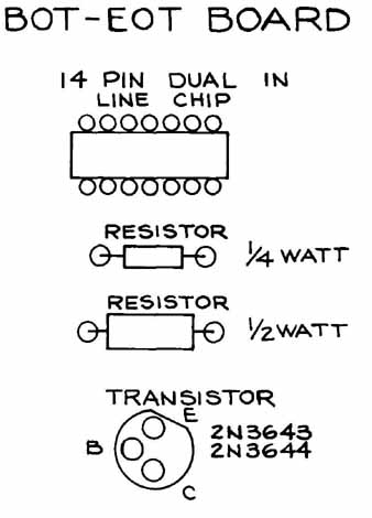
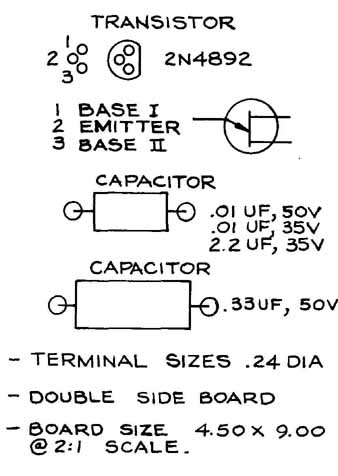
FIG. 37. Design information is given for each component for the BOT-EOT
board.
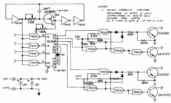
FIG. 38. A typical logic drawing supplied by the engineer. Note: There
are some areas marked out and one ground symbol is incorrect. These are
errors the drafter cleans up. Create a printed circuit board layout from
this and two other drawings.
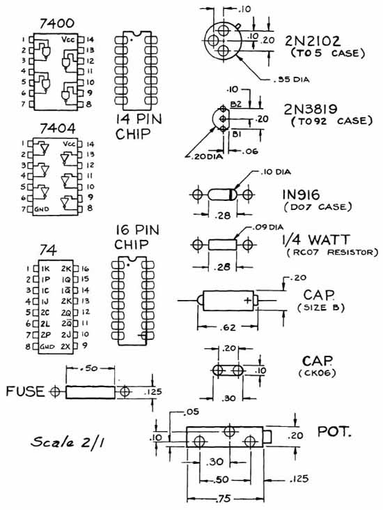
FIG. 39. Component styles for FIG. 38, the logic drawing.
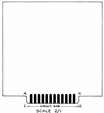
FIG. 40. Board size and connector for FIG. 38.
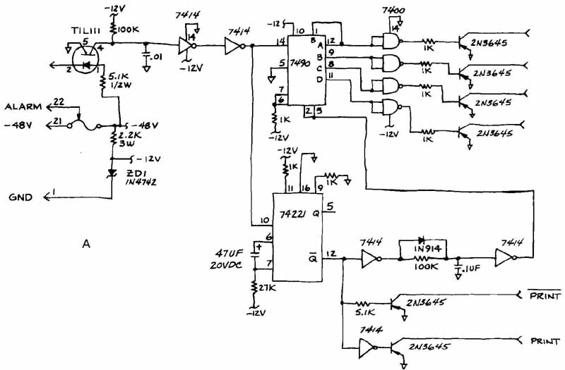
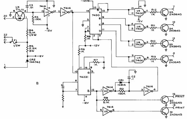
FIG. 41. A—Schematic as submitted to drafting. B—The formal schematic,
which goes with similar board type not using “I, O, Q” when counting
A to N. First, create a formal schematic, then a PCB layout from the
schematic and next drawing.
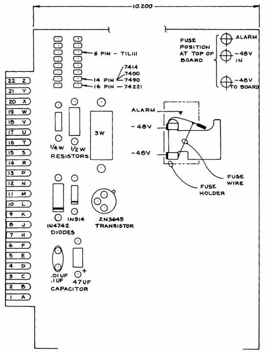
FIG. 42. Components, board size, and connector data for FIG. 41.