AMAZON multi-meters discounts AMAZON oscilloscope discounts
The majority of semiconductor devices are made from silicon (Si), including most transistors, diodes and integrated circuits (ICs). Applications of other semiconductor materials are mostly in specialized areas such as light emitting diodes (LEDs), where compound materials such as aluminum gallium arsenide (AlGaAs) produce red, yellow and green light, and silicon nitride (SiN) blue light. Some very old equipment will still have germanium transistors and diodes, but with the exception of germanium in point contact detector diodes such as the OA47 these have not be used in new designs for more than 20 years. Gallium arsenide finds applications in microwave transistors and very fast logic used in long-haul fiberoptic telecom and supercomputing applications. A relatively recent development is the use of silicon on a germanium substrate for the fabrication of very fast devices.
Silicon, which is found as silicon oxide (sand), is the second most abundant element on Earth; however, the exceptionally high purity of the material needed to make ICs and transistors makes refined silicon very expensive.
Pure silicon on its own does not make a transistor or diode; rather, the sil icon has to have exact small quantities of other elements such as phosphorus (P) or boron (B) diffused into the crystal lattice. The resulting silicon is said to be doped with donor or acceptor atoms; this is because they provide either extra electrons or extra spaces (holes) for electrons, compared with what the pure silicon would have provided. Phosphorus has five valence electrons compared with silicon's four, so it is a donor of electrons, and material doped with phosphorus is said to be N-type. Boron has three valence electrons, so it is an acceptor atom, and silicon doped with it is called P-type. If two regions of different doping are formed so that they have a common boundary it is called a PN junction. The PN junction is the basis of diodes and bipolar transistors, which are referred to as NPN or PNP depending on the junctions that they contain.
Current flowing from the P-type region to the N-type region is called the forward current. The PN junction has an inbuilt potential or threshold voltage below which it will not conduct a forward current; only once an externally applied voltage has overcome the threshold voltage will the diode begin to conduct (FIG. 1). In the reverse direction the diode does not conduct until a breakdown threshold is reached, which is usually 20 or more times the forward threshold.
Although germanium has a lower inherent threshold voltage (100 mV) than silicon, it now finds relatively few applications in modern semiconductor technology. For both germanium and silicon, the reverse biased leakage current of a PN junction approximately doubles for every 11ºC rise in temperature. Since germanium has a significantly higher leakage at room temperature, its operating range is restricted to about 75ºC maximum.
This compares unfavorably with silicon, which can operate effectively up to around 250ºC.
The PN junction threshold voltage for silicon is about 600 mV at room temperature. It falls by about 2 mV per degree Celsius as the temperature rises, so a forward-biased diode can be used a temperature sensor. For example, a 1N4148 diode changes from 750 mV at -55ºC to 350 mV at _150ºC when biased with a current of 200 µA. This can be achieved with a 22 kO resistor and a 5 V supply.
===
Diode current 100mA
_50V Reverse breakdown voltage
Reverse leakage current
Bias voltage =0.6V
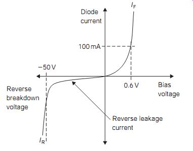
FIG. 1 Typical silicon diode characteristic
===
Base Collector Emitter (a) Base Collector Emitter (b)
FIG. 2 Schematic symbols: (a) NPN, and (b) PNP transistors
====
Bipolar junction transistor
A transistor has three terminals and therefore two PN junctions. The collector and emitter are the connections to the outer layers, while the base is the middle layer. The base is a very thin layer and its function is to control the flow of current between the collector and emitter. The base emitter junction is forward biased to allow current flow between the collector and the emitter; in operation, the collector base junction is usually reverse biased.
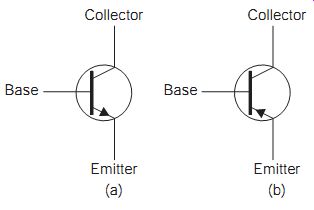
FIG. 2 shows the symbols for NPN and PNP transistors.
Tests with an ohmmeter can identify bipolar junction transistor (BJT) junction faults. A good transistor should have a very high resistance reading between collector and emitter with either polarity of connection.
Measurements between the base and either of the other two electrodes should show one conducting direction and one non-conducting direction. Any variation from this pattern indicates a faulty transistor with either an open-circuit junction (no conduction in either direction) or excessive leakage (conduction in both directions).
The current flowing between the collector and the emitter of a bipolar transistor is much greater than that flowing between the base and the emitter, and the collector current is controlled by the base current. The ratio of collector current to base current is constant (given a constant collector-to-emitter voltage) and is commonly called the current gain for the transistor (its full name is the common-emitter current gain). The symbol used to indicate it is hfe. A low-gain transistor may have a value of hfe of around 20-50, a high gain transistor one of 300-800 or more.
Note that the tolerance of values of hfe is very large, so that transistors of the same type, even transistors coming from the same batch, may have widely different hfe values. Manufacturers often use a gain group code after the part number to make variations within groups easier to deal with; for example, the BC547, which has an hfe range from about 80 to 400, is available in gain groups as BC547A hfe 110-220, BC547B hfe 200-450 and BC547C hfe 420-800.
When one transistor is substituted one for another, the following rules should be obeyed:
• The substitute transistor must be of the same type (i.e. silicon, NPN, switching as opposed to amplifying, etc.).
• The substitute transistor should have about the same hfe value.
• The substitute transistor should have the same ratings of maximum voltage and current.
• When making such substitutions, it is not always possible to guarantee the in-circuit performance of the change.
Bipolar transistors are used as current amplifiers, voltage amplifiers, oscillators and switches. An amplifier has two input and two output terminals, but a transistor has only three electrodes. It can therefore only operate as an amplifier if one of its three electrodes is made common to both input and output circuits.
Any one of a transistor's three electrodes can be connected to perform in this common role, so there are three possible configurations: common emitter, common collector and common base. The three types of connection are shown in FIG. 3(a-c).
The normal function of a transistor when the base-emitter junction is for ward biased and the base-collector junction is reverse biased, is as a current amplifier. Voltage amplification is achieved by connecting a load resistor (or impedance) between the collector lead and the supply voltage (FIG. 3a). Oscillation is achieved when the transistor is connected as an amplifier with its output fed back, in phase, to its input. The transistor can also be used as a switch when the small base-emitter junction current is used to switch on the larger collector current.
The three basic bipolar transistor circuit connections are shown in FIG. 3, with applications and values of typical input and output resistances given below each. The common-collector connection in FIG. 3(b), with signal into the base and out from the emitter, is used for matching impedances, since it has a high input impedance and a low output impedance. The common-base connection, with signal into the emitter and out from the collector (FIG. 3c) is often used for ultra high-frequency (UHF) amplification, for example in television mast head amplifiers.
The graph of a typical transistor IC versus VCE for different values of base current (FIG. 4) shows how the base current can be used to control the transistor collector current; for example, changes in the collector voltage can be seen to have only relatively small effects on the collector current, implying a high output resistance.
===
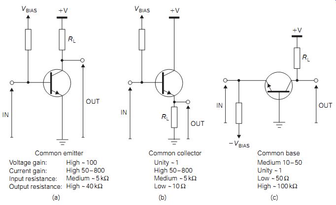
FIG. 3 The three circuit connections of a bipolar transistor
===
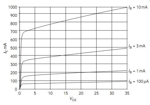
FIG. 4 Typical small signal NPN transistor characteristic
Transistor failure
When transistors fail, the fault is either a short-circuit (s/c) or an open-circuit (o/c) junction; or the failure may possibly be in both junctions at the same time. An o/c base-emitter junction makes the transistor 'dead', with no current flowing in either the base or the collector circuits.
When a base-emitter junction goes o/c, the voltage between the base and emitter may rise higher than the normal 0.6 V (silicon) or 0.2 V (germanium), although higher voltage readings are common on fully operational power transistors when large currents are flowing. An s/c base-emitter junction will allow current to flow easily between these terminals with no voltage drop, but with no current flowing in the collector circuit.
The two above faults are by far the most common, but sometimes a base collector junction goes s/c, causing current to flow uncontrollably. The base region of a bipolar device can be ruptured through the application of an excessively high collector voltage, this is often described as punch-through.
All of these faults can be found by voltage readings in a circuit, or by use of the ohmmeter or transistor tester when the transistor is removed from the circuit. (Transistor testers are now available that allow in-circuit testing.)
===
Source
Source Gate
Gate Drain
Drain Aluminum SiO2 Induced channel Substrate (a) (b)
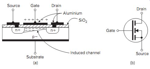
FIG. 5 MOSFET principles, N-channel device: (a) basic construction,
and (b) schematic symbol
====
Field-effect transistors
The BJT relies for its action on making a reverse-biased junction conductive by injecting current carriers (electrons or holes) into it from the other junction. The principles of the field-effect transistor (FET) are entirely different.
In any type of FET, a strip of semiconductor material of one type (P or N) is made either more or less conductive because of the presence of an electric field pushing carriers into the semiconductor or pulling them away.
There are two types of FET: the junction field-effect transistor (JFET) and the metal oxide semiconductor field-effect transistor (MOSFET). Both work by controlling the flow of current carriers in a narrow channel of semi conductor, usually silicon. The main difference between them lies in the method used to control the flow. Since the JFET is now a device that is rarely used in consumer electronics except for high-end audio preamplifiers, we shall concentrate on the much more common MOSFET.
FIG. 5(a) shows the basic construction of a MOSFET. A silicon layer, called the substrate or base or sometimes bulk, is used as a foundation on which the FET is constructed. The substrate is lightly doped and may have a separate electrical connection, but it generally takes no part in the FET action and if a separate electrical connection is provided it is usually connected to the source, forming a reverse-biased diode between source and drain under normal operating conditions. Two heavily doped regions, of opposite polarity to the substrate, forming the source and drain, are then dif fused into the top surface of the substrate, and an insulating layer of silicon dioxide (SiO2) is grown over the surface. In the example, the substrate is of P-type silicon, and the source and drain are of N-type, so there is no conducting path between the N-type source and drain regions.
The gate is insulated from the channel by a thin film of silicon dioxide, obtained by oxidizing the surface of the silicon, and a metal film is deposited over this insulating layer to form the gate. Before deposition the metal film holes are etched in the SiO2 above the drain and source diffusions so that aluminum contacts can be made to the diffused regions.
For an N-channel MOSFET with a gate-to-source voltage equal to zero, the device is cut off. When a gate voltage that is positive with respect to the substrate is applied, an electric field is set up that attracts electrons towards the oxide layer. These now form an induced channel to support a current flow. An increase in this positive gate voltage will cause the drain-to-source current flow to rise (FIG. 6). A negative voltage so applied would repel any electrons from the channel and so reduce its conductivity.
If a positive voltage is applied to the gate of an N-channel device, it has the effect of attracting electrons into the region between the source and drain under the gate electrode. This is the same effect as observed in charging a capacitor; that is, current flows into the gate of the MOSFET until the gate capacitance is fully charged. This charging current can be quite high, and the rate at which current can be moved into and out of the gate limits the speed at which the device can be turned on or off.
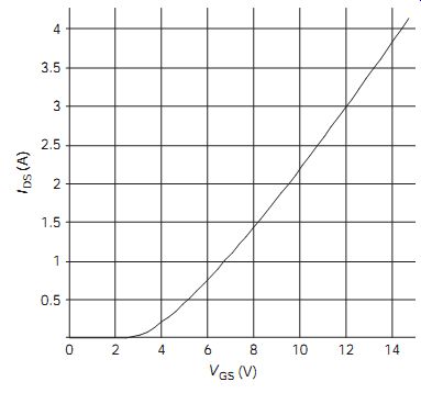
FIG. 6 Drain current dependence on gate voltage for typical medium-power
N-channel MOSFET
Both N-channel and P-channel devices can be made. In addition, the channel can be either lightly or heavily doped with the same polarity as the source and drain. In this case there will be a conducting path of fairly low resistance between the source and the drain when no bias is applied to the gate. Such a device is usually operated with a bias on the gate that will reduce the source-drain current, and is said to be used in depletion mode.
When the channel is formed from lightly doped or substrate material it is normally non-conducting, and its conductivity is increased by applying bias to the gate in the correct polarity, using the FET in enhancement mode. Enhancement-mode operation is more common.
Small-signal MOSFETs need to be handled with great care because the gate is completely insulated from the other two electrodes by the thin film of silicon oxide. This insulation will break down at a voltage of 20-100 V, depending on the thickness of the oxide film. When it does break down, the transistor is destroyed. Any insulating material that has rubbed against another material can carry voltages of many thousands of volts, and lesser electrostatic voltages are often present on human fingers. There is also the danger of induced voltages from the a.c. mains supply.
Voltages of this type cause no damage to bipolar transistors because these devices have enough leakage resistance to discharge the voltage harmlessly. The high resistance of the MOSFET gate, however, ensures that electrostatic voltages cannot be discharged in this way, so that damage to the gate of a MOSFET is always possible.
To avoid such damage, most MOSFET gates that are connected to external pins of ICs of power MOSFETs are protected by diodes, which are created as part of the IC or FET during manufacture and have a relatively low reverse breakdown voltage. These protecting diodes will conduct if a voltage at a gate terminal becomes too high or too low compared to the source or drain voltage level, so avoiding breakdown of the insulation of the gate.
The use of protective diodes makes the risk of electrostatic damage very slight for modern MOS devices, and there is never any risk of damage to a gate that is connected through a resistor to a source or drain unless excessive d.c. or signal voltages are applied. Nevertheless, it is advisable to take precautions against electrostatic damage, particularly in dry conditions and in places where artificial fibers and plastics are used extensively. These pre cautions are:
• Always keep new MOSFETs with conductive plastic foam wrapped round their leads until after they have been soldered in place.
• Always short the leads of a MOSFET together before unsoldering it.
• Never touch MOSFET leads with your fingers.
• Never plug a MOSFET into a holder when the circuit is switched on.
MOSFETs can be used in circuits similar to those in which bipolar transistors are used, but they give lower voltage gain and are only used singly when their peculiar advantages are required. They are extensively used in ICs, however, because of their low power dissipation and the ease of forming very large numbers of MOSFETs on a silicon chip. In circuit applications, MOSFETs have the following advantages:
• MOSFETs have a very high input resistance at the gate, a useful feature in voltmeter amplifiers.
• MOSFETs perform very well as switches, with channel resistance switching between a few hundred milliohms and several mega-ohms as gate voltage is varied.
• The graph of channel current Ids, plotted against Vgs, the voltage between the gate and the source, is noticeably curved in a shape called a square law. This type of characteristic is particularly useful for signal mixers in superheterodyne receivers.
Double-gate MOSFETs are used as mixers and as radio frequency (RF) amplifiers in frequency modulation (FM) receivers. The shape of MOS characteristics can provide less distortion in linear power amplifiers, and high power FETs are available for use in high-quality audio equipment.
MOSFET failure is almost always caused by breakdown of the insulating silicon oxide layer. In either case, gate voltage can no longer control current flow in the channel between source and drain, and pinch-off (the cut off condition) becomes impossible. In addition, if very large currents have been allowed to flow between source and drain, the channel may overheat and rupture.
Four-layer devices
This topic covers a range of related semiconductor devices that are basic ally four-layer PNPN sandwiches designed either for a.c. or d.c. switching purposes.
The thyristor is a commonly used switching device, and often referred to as a silicon-controlled rectifier (SCR). It is fabricated as four doped layers, and its symbol and schematic construction are shown in FIG. 7. Only three of the four semiconductor layers have external connections.
===
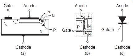
FIG. 7 Silicon-controlled rectifier: (a) typical arrangement of layers,
(b) equivalent circuit, and (c) symbol
===
When the gate voltage is zero, the device offers high resistance irrespective of the polarity of the anode-to-cathode voltage, because at least one PN junction is always reverse biased. Even when a thyristor is forward biased, with the anode positive with respect to the cathode, it will only be driven into conduction when its gate is forward biased sufficiently.
With the anode voltage positive with respect to the cathode, the action is controlled by the gate voltage. Briefly applying a positive voltage (Vg) to the gate causes the thyristor to go into conduction (between anode and cathode) and then remain in this state even if Vg is removed. Turn-off is achieved by briefly reducing the anode current below some threshold value, typically a few milliamps. The device can carry several tens of amps at several hundreds of volts. Referring to the equivalent circuit (FIG. 7b), we can see that once the gate (base of the NPN transistor) is turned on the device latches because the gate current is supplied by the top (PNP) transistor's collector. From this, it can also be deduced that to turn off the device the gate current must be reduced below the holding threshold.
Once it has been switched on in this way, the thyristor will remain con ducting until either:
• the voltage between anode and cathode falls to a small fraction of a volt; or
• the current flow between anode and cathode falls to a very low value.
The important ratings for a thyristor are its maximum average current
flow, its peak inverse voltage, and its values of gate-firing voltage and current. A small thyristor will fire at a very small value of gate current, but a large one calls for considerably greater firing current (1 A or more).
The silicon-controlled switch (SCS) is constructed in a very similar way to the SCR, is self-latching and functions in a similar way for turn-on, but is turned off by either reducing the anode current or reverse biasing the gate to cathode junction.
====
Connect up the circuit of FIG. 8. Any small thyristor such as 2N5060 or TIC106D will be suitable. The purpose of the lamp bulb is to indicate when the thyristor has switched on, and limit the current once it has turned on. Use a d.c. supply as shown, increase the gate voltage from zero, measure the gate voltage and load current until the thyristor fires. After the lamp lights, disconnect the gate circuit, and note that this has no effect. Switch off the power supply, and then switch on again. The lamp will not now light because the thyristor has switched off. Repeat the operation, this time using an unsmoothed rectified a.c. supply. The thyristor now switches off when the gate voltage is switched off, because the unsmoothed supply reaches zero voltage 100 times per second (assuming a full-wave rectified 50 Hz supply).
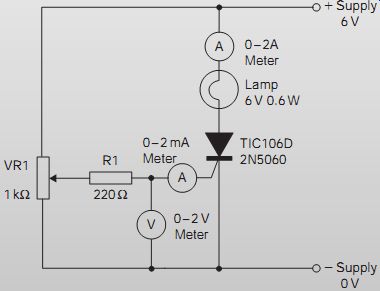
FIG. 8 Circuit for practical
===
Thyristors are used for power control, using either a.c. or an unsmoothed rectified supply. By being made to fire at different points in each a.c. cycle, the thyristor can be made to conduct for different percentages of the cycle, thus controlling the average current flow through the load. This is called phase control of the duty cycle.
An alternative method used for slow-changing load conditions, such as in furnace temperature control, fires the thyristor into conduction for several a.c. cycles and then drives into cut-off for several further cycles. The aver age power in the load can be controlled by altering the ratio of conducting cycles to non-conducting cycles. This technique is known as burst control.
The gate turn-off thyristor (GTO) is an alternative device which is triggered on by a positive pulse of fairly high current (typically 100 mA) and triggered off by a negative pulse of lower current, both pulses being applied to the same gate.
The tetrode thyristor is equipped with both anode and cathode gates to provide a self-latching action. The turn-on action is achieved by driving the cathode gate positive or the anode gate negative, and the device is turned off by reversing the gate potentials.
====
Connect up the thyristor circuit illustrated in FIG. 9, and switch on. Use the potentiometer to control lamp brightness by altering the time in the cycle at which the thyristor fires. Note that an unsmoothed full-wave rectified supply is essential.
EXPERIMENT 2
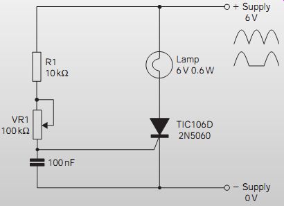
FIG. 9
Circuit for practical
====
Failure of a thyristor can be caused by an open-circuit gate, or by internal short-circuits. When the gate is o/c, the thyristor will fail to conduct at any gate voltage. When an internal short-circuit is present, the thyristor acts like a diode, conducting whenever the anode is more than 0.6 V positive with respect to the cathode, so making control impossible. A completely short circuit thyristor is able to conduct in either direction, with similar total loss of control.
Thyristor circuits often include a low-pass filter (called a snubber circuit) consisting of an inductor and capacitor or resistor and capacitor in the anode circuit, to suppress the RF interference caused by the sudden switch on action of the thyristor.
A triac is a two-way thyristor which, when triggered, will conduct in either direction. The terminals are labeled M1, M2 and Gate (the words 'anode' and 'cathode' cannot be used in this case because the current can flow in either direction). The gate can be triggered by a pulse of either polarity, but the most reliable triggering is achieved when the gate is pulsed positive with respect to M1.
In most triac circuits, M1 and M2 have alternating voltages applied to them, so that the gate must receive the same waveform as M1 when it is not being triggered. To trigger the gate, a pulse must be added to the waveform already present, and this is most easily done by using a pulse transformer driven by a trigger circuit. The transformer being used to isolate the triac works at line voltage, from the low-voltage control circuit. FIG. 10(a) shows the symbol for a triac.
A diac is a two-terminal trigger device fabricated as a gateless triac that triggers by breakdown at a designed low voltage and is often used in the gate circuit of a thyristor or triac. FIG. 10(b) shows the schematic symbol for the diac. At low voltages or either polarity, a diac is completely non-conducting; however, once its breakdown threshold is reached it can conduct in either direction.
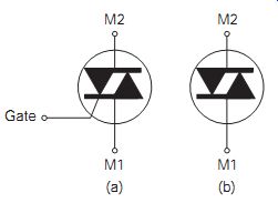
FIG. 10 (a) Triac symbol, and (b) diac symbol
When a diac is used, the gate of the thyristor can be connected to the cathode by a low-value resistor to avoid accidental triggering. In addition, if the triggering waveform rises slowly, the diac will ensure that the thyristor is switched on by a fast rising pulse of current, so avoiding uncertain triggering times.
• The causes of failure in triacs are the same as they are for thyristors.
The advantages of using thyristors and triacs for power control are:
• Both thyristor and triac are switched either completely off, with no current flowing, or fully on, with only a small voltage between the terminals. Either way, very little power is dissipated in the semiconductor, so that heat sinks are required only for devices that handle a substantial amount of power.
• Operation can be either at line or at higher frequencies, unlike relays or similar electromechanical switches.
• Thyristors and triacs are 'self-latching', which means that they stay conducting once they have been triggered. A relay, by contrast, needs a current passed continuously through its coil to keep it switched over, and relay latching circuits require additional relay contacts.
Thyristors and triacs are used as solid-state relays, allowing a small voltage and current to switch a much larger voltage and current. Unlike a relay, however, there is no electrical isolation between the trigger circuit and the main supply unless a suitable transformer is used, so that some applications call specifically for a relay to be used in place of any semiconductor device.
FIG. 11 shows a typical circuit using a triac to control the power to a 60 W lamp. The potentiometer adjusts the charging current to the capacitor, so determining at what part in each half-wave the voltage across the diac will be enough to cause conduction and so fire the triac.
===
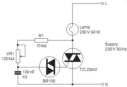
FIG. 11 Typical triac and diac use in a mains lamp dimmer
====
HAZARD - high voltages: triac lamp dimmers like that of FIG. 11 are connected to mains potential; when working on such circuits, the circuit must be supplied from an isolating transformer, and all live parts of the circuit should be covered to protect against accidental contact.
Transducers
A transducer is a device that converts energy from one form to another. The transducers that are of most interest as far as electronics is concerned are those in which one of the energy forms is electrical energy. Of the many possible transducers, the most common are the transducers for light, heat and sound.
The transducers that involve light are known as electron-optical devices.
Photoelectric transducers convert light energy into electrical signals and are widely used in the communications and measurement environments.
They are used extensively in position sensing and counting devices where the interruption of a light beam is converted into an electrical signal. As most of these devices have a wavelength response greater than the human eye, their applications extend into the infrared region. Two main principles can be used: photoconductivity and photovoltaic effect.
Light-dependent resistors
The resistance of certain materials that are used for light-sensitive devices decreases when subjected to increased illumination. This is a photoconductive effect. The common materials used for light-dependent resistors (LDRs) include selenium, cadmium sulphide, cadmium selenide and lead sulphide. Each material responds to different wavelengths of light. FIG. 12(a) shows the general appearance of a photoconductive cell and its construction. Gold-conducting sections are deposited on a glass plate with a long, meandering gap to isolate the two sections. A thin layer of suitable photo conductive material is then deposited to bridge the insulating region. This construction is necessary to reduce the cell's resistance to a usable value.
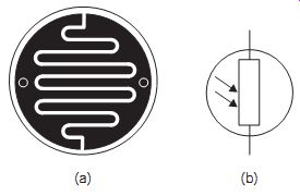
FIG. 12 (a) Typical photoconductive cell, and (b) schematic symbol
Typical resistance values for various cells range from about 500 K to 10 M in darkness and from about 1 K to 100 K in bright light. The change in resistance is non-linear and there is a significant time lag (up to 0.1 s) in response to a pulse of light.
Typically, LDRs are used in series with a fixed resistor or potentiometer, to form a potential divider whose ratio is dependent on the light level.
Increasing the illumination of the LDR lowers its resistance so that the output voltage changes. The maximum permitted voltage for these cells may be as high as 300 V and the maximum power dissipation is in the order of 300 mW. The dark-to-light resistance ratio ranges from about 50:1 to 250:1. These cells can often be used directly without amplification, to trigger a triac in applications such as dusk-to-dawn switches.
The cells are particularly sensitive to red light and the infrared wave lengths, so they are often used as flame detectors in boiler and furnace control systems. Application of an excessive voltage or current is the most common cause of failure.
Photodiodes
Photodiodes are very similar to a normal PN junction device. They are formed with one very thin region and equipped with a lens so that light energy can be directed into the depletion region. When this happens, hole-electron pairs are generated to increase the diode's conductivity. Such diodes have a peak response in the infrared region, but the response to visible light is still very useful.
The diodes are operated either reverse biased, or only very slightly forward biased (to increase sensitivity) so that no current flows. Typical dark current is as low as 2 nA, rising to about 100 µA in bright light for germanium types.
Modern PIN silicon [a PN junction with an additional interposed layer of intrinsic (I)-type, meaning undoped] semiconductors may have a peak power dissipation greater than 100 mW.
The increase in current due to the light is practically linear. The response time to a pulse of light is very short, so they find applications in high-speed switching circuits. In general, the small output is a disadvantage and amplification is needed. The basic circuit configuration is shown in FIG. 13.
===
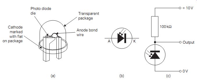
FIG. 13 Photodiode: (a) package, (b) symbol, and (c) typical circuit :
Note: Anode bond wire; Transparent package
===
Phototransistors
A phototransistor has a similar construction to a silicon planar transistor, except that it is equipped with a lens so that light can be made to shine directly into the base-emitter junction. Their response time to a pulse of light is in the order of 1-2 µs and they are therefore mostly used in medium speed light detector circuits. The current ranges from about 25-50 µA in darkness to about 5-10 mA in bright light.
The phototransistor (FIG. 14) is connected so that the base is open circuit, reversed biased or only very slightly forward biased. In some devices, the base connection is omitted altogether, so only the collector and emitter connections can be used. The load may be placed in either the collector or emitter leads as shown (left). Light shining into the base-emitter junction modulates the base current, which is in turn magnified by the current gain. Such a device can be used to drive a load directly, as shown in the relay-load example.
Light-emitting diodes
The operation of the photodiode depends on the application of energy to generate hole-electron pairs. The reverse action is that when holes and electrons recombine, energy is released. In germanium and silicon, this energy is released as heat into the crystal structure. However, in materials such as gallium arsenide and gallium phosphide this energy is released as visible light, and different semiconductor compounds release light of different wavelengths (colors). For example, infrared LEDs are made from silicon.
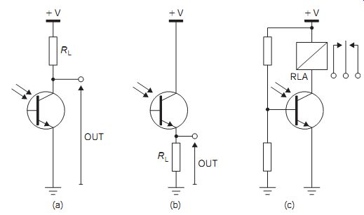
FIG. 14 Phototransistor use: (a) collector load, (b) emitter load,
and (c) driving a relay (back-emf diode omitted)
The basic structure of the diode is shown in FIG. 15(a). The plastic moulding not only holds the component parts together, but also acts as a light pipe so that most of the light generated is radiated from the domed region.
===
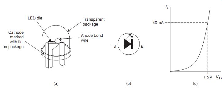
FIG. 15 (a) Typical packaged LED, (b) symbol, and (c) forward characteristic
===
A characteristic typical of an LED is shown in FIG. 15(c). When forward biased beyond about 1.6 V, the current rises rapidly and light is released. The current should be limited to a value less than about 40 mA by the use of a series resistor. In addition, the LED must not be reverse biased to more than a fraction of a volt, and circuits are often designed to avoid any possibility of reverse bias.
Opto devices
The optocoupler consists of an LED and phototransistor pair whose symbol is illustrated in FIG. 16. The input signal modulates the diode current and hence the intensity of its (usually infrared) light output. This variation in light produces a variation in collector current to provide an output signal. Since the light beam has no electrical impedance, there are no matching problems between input and output circuits. The electrical isolation is very high, and an optocoupler can withstand test voltages as high as 4 kV between input and output terminals. Alternatively, an LED can be used to launch energy into a glass optical fiber cable to transmit the signal over very much greater distances. A variation of the optocoupler is the slotted opto-switch (FIG. 16c). The light path between the LED and the photo diode can be interrupted by a shutter, generating a pulsating signal as the shutter breaks the beam of infrared light, which could be used to drive a counter-circuit, for example.
Photodiodes and transistors have similar fault tolerance to conventional semiconductors. Excessive voltage, current or temperature are the common causes of failure. Faulty devices can be located using the same techniques as applied to other semiconductors.
Laser diodes are used in many applications, from CD and DVD players to laser pointers, laser spirit levels and laser printers. The typical construction of a low-power laser diode of the type used in many of these applications is shown in FIG. 17(a).
===
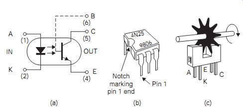
FIG. 16 Optocoupler: (a) symbol, (b) typical
six-pin dual in line (DIL) package, and (c) typical slotted optoswitch
package
===
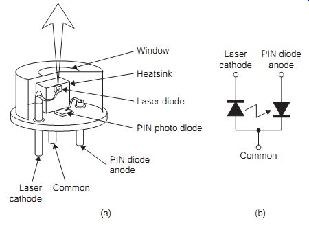
FIG. 17 (a)
Typical laser diode construction, and (b) schematic symbol
===
Warning: laser radiation can permanently damage your eyesight. Always observe the precautions on labels and in manufacturers' handbooks: never attempt to look directly at any sort of laser that is potentially turned on. Remember that although infrared light is invisible it can still damage your eyes. The symbol warning of laser radiation is shown in FIG. 18. You will find this on CD players, laser printers and many other devices that use lasers.
CAUTION! Laser beam! Do not look into the beam; Max output 1mW at 650 nm; class 2 laser product
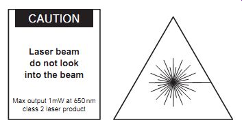
FIG. 18 Laser radiation warning symbol
Typical laser diode applications that require a continuous output use feed back from the photodiode mounted in the same package (FIG. 17) to close the loop of an automatic power control (APC) drive circuit. When the laser diode emits light, the photodiode current is proportional to light output power. This current is then used to control the drive to the laser diode, and this enables a constant output power to be maintained. Without such a power control circuit laser diodes can be vulnerable to thermal runaway and self-destruction. In pulsed applications the photodiode power control circuit is not always required, but is often necessary to reduce the effects of temperature, etc., on the output level.
Photovoltaic devices
In the classic type of photovoltaic cell, as used in camera light meters and similar devices, a layer of selenium is deposited on an iron or aluminum backing plate which forms the positive pole. A transparent layer of gold is evaporated onto this to form the negative pole. A metallic contact ring completes the circuit.
Light shines through the gold film into the layer of selenium. This releases electrons that form an electric field within the selenium, making the gold layer the negative pole of the cell. The whole cell is enclosed in a plastic housing with a transparent window for protection. The maximum current in bright light depends on the particular cell, but short-circuit currents in excess of 1 mA can be obtained. Such cells are suitable to drive a portable photo graphic light meter.
The majority of solar cells in use are silicon photovoltaic cells. These cells are typically manufactured by sawing lightly doped P-type silicon ingots into thin slices. The front surface of the slice has N-type material diffused into it to form a vertical P-N junction. The back of the slice is metallized usually with aluminum, and a grid or trellis structure of aluminum connections is deposited onto the front N-type surface (FIG. 19a). Connections to these metal areas provide a way of collecting current from the cell. A cell of about 4 cm^2 is capable of providing 0.6 V on open circuit, with a short circuit current of up to 100 mA in bright light. The cells can be connected in a series-parallel configuration to provide a greater output power level. The cost of manufacturing such cells has fallen steadily, and they are used extensively to provide power for applications as diverse as garden lighting and remote weather monitoring stations.
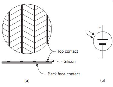
FIG. 19 (a) Silicon
solar cell, and (b) schematic symbol
Temperature sensors
Semiconductor diodes can be used as temperature sensors, as mentioned previously; however, they are typically only useful at low currents and over a relatively narrow temperature range, between about -60 and +180ºC. Other temperature sensors can carry much higher currents: thermistors or thermocouples can operate at temperatures up to about +1300ºC.
Thermistors
The thermistors may be in rod, bead, washer or disc form. Thermistors are made from carefully controlled mixtures of certain metallic oxides.
These are sintered at very high temperatures to produce a ceramic finish.
Thermistors have a large temperature coefficient of resistance, and it is this that makes them useful as a temperature sensor Negative temperature coefficient (NTC) thermistors have resistances that fall with a rise in temperature, and are commonly made from mixtures of the oxides of manganese, cobalt, copper and nickel. Positive temperature coefficient (PTC) components, whose resistance increases with a rise in tempera ture, can be made from barium titanate with carefully controlled amounts of lead or strontium.
===
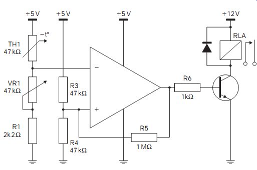
FIG. 20 Typical temperature measuring circuit using thermistors
===
Thermistors are used extensively for temperature measurement and control up to about 400ºC. A typical heater controller (thermostat) circuit using an NTC thermistor is shown in FIG. 20, in which the comparator circuit switches at some temperature set by the variable resistor VR1. Th1 is in good thermal contact with the object being heated. When the circuit is turned on (cold) the thermistor resistance is very high, so the voltage at the comparator inverting input is lower than the non-inverting input and the transistor is turned on, pulling in the relay contact and operating the heater. As the temperature rises the thermistors resistance falls, and a point is reached where the input to the comparator inverting input exceeds the non-inverting input voltage. The comparator turns off the transistor and heater. R5 provides hysteresis, feeding back a signal from the output to change the threshold of the switching point. This prevents the circuit from oscillating near the set point. Look at the circuit and calculate the voltage at the non-inverting input of the comparator for both the heater on and off case.
Another application of thermistors is to provide temperature compensation for the change in the winding resistance of alternators and other generators, which affects their performance when the operating temperature rises.
Similarly, NTC thermistors are used as in rush suppressors, to protect the cathode heater of a cathode-ray tube (CRT) at switch-on.
===
Iron Thermo junction Thermo junction Constantan (Cu Ni alloy) Reference junction (cold junction) Insulated twisted pair of metal wires Stainless steel probe Thermo junction (insulated from probe body) Beaded thermo junction Measurement junction T2 V (a) (b) (c) T1
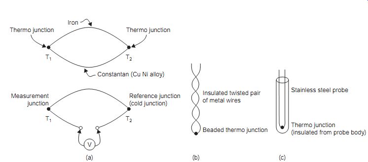
FIG. 21 (a) Principle of a thermocouple junction, (b) construction
of beaded junction sensor, and (c) construction of rod probe
===
Thermoelectric transducers
When two dissimilar metals are in contact with each other a contact potential is developed between them. This is known as Seebeck or thermoelectric effect. The voltage, which rises with temperature, is almost linear over several hundred degrees. If two junctions are formed as shown in FIG. 21(a), making a thermocouple, a current will flow around the circuit provided that each junction is at a different temperature. The circuit can be modified to include a meter which measures the difference in potential between the junctions. Accurate measurements can be made by holding one junction at a known temperature, usually the melting point of ice (hence called the cold junction), while the other becomes the temperature sensor. The two metals are chosen to maximize the contact potential for a particular temperature range. The cold junction in most applications is simulated by a semiconductor circuit called a cold junction compensator, rather than using a bucket of melting ice.
The metals used include:
• iron and copper/nickel alloy
• copper and copper/nickel alloy
• nickel/chromium alloy and copper/nickel alloy
• nickel/chromium alloy and nickel/aluminum/manganese alloy.
Thermocouples allow for a range of instruments to measure temperatures from -85ºC to 2000ºC. For most temperature measurements, the hot junction is formed into a probe, either a low-cost bead on the end of a twisted pair of insulated wires (FIG. 21b) or with a metal sheath (FIG. 21c) to protect the junction from environmental hazards, and electrically isolated from it with magnesium oxide. This material has good thermal conductivity with high electrical resistance (up to 1000 M).
As noted earlier in this section, a temperature sensor can be based on the behavior of a silicon diode. When a silicon diode is forward biased to operate at a constant current, its junction temperature changes linearly at a rate of -2 mV/ºC. Therefore, this device can be used as a temperature-to-voltage transducer, where the output voltage can be used to indicate temperature.
Magnetic field sensors; the Hall effect
When a moving charge is exposed to a magnetic field, the path of the charge is deflected by interaction with the magnetic field. Current flow is due to a net movement of charge carriers, and the current carriers flowing within the conductor are deflected by magnetic field. Therefore, a voltage develops across the width of the conductor, and as a result a mechanical reaction occurs which tends to cause the conductor to move.
In normal conductors this voltage difference effect is of no practical importance, but when a magnetic field is applied to semiconductor materials, the amount of generated voltage becomes significant. It is put to practical use in a group of semiconductors called Hall-effect devices, illustrated in schematic form in FIG. 22.
A Hall-effect device consists of a very small (about 2 _ 2 _ 0.5 mm) slab of gallium arsenide, indium antimonide or silicon onto which two pairs of electrodes are evaporated (FIG. 22). A control current I and a magnetic field B are applied as shown, and the Hall voltage VH is generated in a direction at right angles to both of them. The value of VH is proportional to both the current I and the strength of the magnetic field B, depending on the dimensions and nature of the semiconductor material.
With a constant current passing, the Hall voltage is directly proportional to the strength of the magnetic field. The first and most obvious application for the device is therefore the measurement of the field strengths of both permanent magnets and electromagnets. It is also used in conjunction with switching transistors in brushless d.c. electric motors; by eliminating the mechanical brush gear that is so prone to wear, the reliability is improved.
The device can also be used in contactless switches, where the movement of a permanent magnet sets up the Hall voltage, which in turn triggers a semiconductor switch.
When the application of the magnetic field in the Hall-effect device deflects the current carriers to one side of the conductor, they are caused to flow through a smaller cross-sectional area. This increases the effective resistance of the device, and so reduces current flow. This type of application is the magnetic-dependent resistor (MDR). Over a normal range of magnetic fields strengths, device resistance can in this way be made to vary by a factor of about five. One particularly useful application of an MDR is in the 'clamp-on' type of current meter used to measure current flow in power supplies drawing power directly from the electrical mains.
===
V Hall voltage Current source Magnetic field
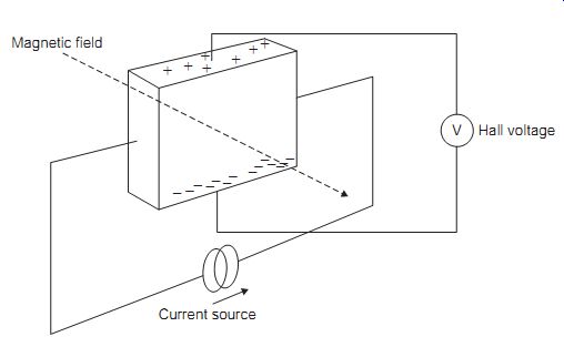
FIG. 22 Schematic diagram of the Hall effect
===
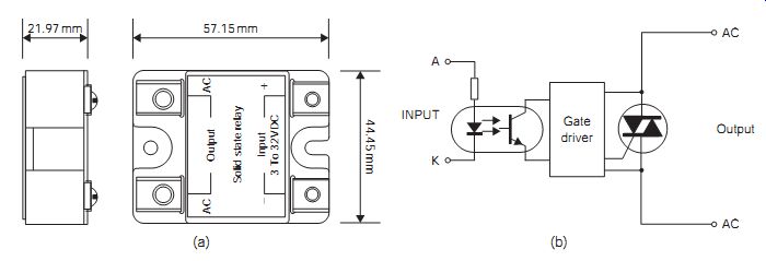
FIG. 23 (a) Typical solid-state relay package, and (b) simplified
circuit
===
Solid-state relays
Solid-state relays are typically used in mains power control applications where low-voltage devices such as microprocessors are required to operate high-voltage, high-current equipment. Typically having an optically isolated input stage (FIG. 23) and triac or dual thyristor zero-crossing switched output stage makes solid-state relays much more reliable than their mechanical equivalents. Output current ratings of 10-125 A at 230 V r.m.s. are commonly available.
Electrostatic discharges
Lightning and ionospheric storms are the chief sources of high levels of electrostatic discharge (ESD), but artificial electrostatic charges are rather more subtle. These can be generated by the rubbing together of two dissimilar materials. Actions such as walking across a carpet or even the nature of the clothing worn can give rise to tribo-electricity, as this phenomenon is known.
The discharge of static electricity can easily damage MOSFETs, complementary metal-oxide semiconductors (CMOS) and group III/V compound semiconductor (GaAs, etc.) devices. A discharge from a potential difference as low as 50 V can cause component degradation, and since the effect is cumulative, repeated small discharges can lead to ultimate failure. It is therefore important that any sensitive equipment should be serviced in a workshop where static electricity can be controlled. Bipolar transistors are rather more robust in this respect.
Note: this is usually a problem only when individual devices or modules such as computer memory are being handled. Devices that are wired into a circuit usually have comparatively low resistance between electrodes, so damage is unlikely. The problem is much more acute for manufacturers than for service personnel, particularly since much of the servicing of circuits that contain components liable to ESD dam age will be done by replacing modules rather than individual devices.
For working with such components the basic workstation should provide for operators, workbench, floor mat, test equipment and the device under service to be at the same electrical potential. Operators should be connected to the workbench via a wrist strap. To avoid static electricity the operator's clothing also needs to be considered. The wearing of wool and artificial
fibers such as nylon creates considerable static. One very useful garment is a smock made of polyester fabric, interwoven with conductive carbon fibers.
This has through-the-cuff earthing. The use of compressed air to clean down boards can generate static and this can be avoided by the use of an ionized air blast.
Static-sensitive components should be stored in conductive film or trays until required and then handled with short-circuited leads until finally in circuit. Soldering iron bit potentials can also be troublesome unless adequately earthed. The workbench surface should be clean, hard, durable and capable of dissipating any static charge quickly. These static-free properties should not change with handling, cleaning/rubbing or ambient humidity.
The use of an ionized air ventilation scheme can be an advantage. Large quantities of negatively and positively charged air molecules can quickly neutralize unwanted static charges over quite a significant area. Capacitors, including the capacitance of CRTs, should not be discharged too rapidly, to avoid damage through excessive current flow. Normal power supply capacitors can be safely discharged through a 250 V rated 0.5 W 1 K resistor, but for the extra high tension (EHT) voltages found on the CRT, it is safer to use a 100 K resistor.
QUIZ:
Q-1. A transistor has a stated value of hfe equal to 150. What base current (in microamps) would you expect to produce a collector current of 60 mA?
(a) 150 µA
(b) 400 µA
(c) 60 mA
(d) 9 A.
Q-2. A circuit operating from a 5 V supply uses a silicon bipolar transistor in common emitter configuration to turn on a relay. What is the base emitter voltage when the relay is on?
(a) 0 V
(b) 0.2 V
(c) 0.6 V
(d) 5 V.
Q-3. To turn off a P-channel enhancement MOSFET, the gate voltage must be?
(a) equal to the drain voltage
(b) higher than the source voltage
(c) lower than the source voltage
(d) 0 V.
Q-4. What is the gate-cathode voltage is required to turn on a thyristor (SCR)?
(a) 0.6 V
(b) 1 V
(c) 6 V
(d) 230 V.
Q-5. A light-dependent resistor is use to turn on a night light at dusk. What resistance would you expect it to have in bright sunlight?
(a) >10 MO
(b) <1 O
(c) < 100 kO
(d) 50 O.
Q-6. A red LED is to be operated from a 13.82 V supply. If it has a VF of 1.6 V and must draw 20 mA from the supply, what resistor would you use to limit the current?
(a) 220 O
(b) 390 O
(c) 820 O
(d) 10 kO.