AMAZON multi-meters discounts AMAZON oscilloscope discounts
From a customer or user's perspective, quality is a measure of fitness for purpose, as a measure of the reliability and the ease of use and efficiency of the product. From a manufacturing perspective, quality is often defined as a measure of how well a product or system conforms to its claimed specification. Reliability is then a measure of how long the product or system continues to meet this specification. Quality and reliability are of great interest to the end user because they directly affect their confidence that the product or system will meet their expectations. To meet both manufacturers' and customers' definitions it is usual for products to be designed in a quality assured environment. Quality assurance is the management of the design and manufacturing processes in such a way as to build in quality. As part of quality assurance it is necessary to measure the manufacturing yield and field returns, among other parameters; these parameters can be evaluated statistically to provide the evidence necessary to maintain or improve the quality of the product.
Quality control is the measurement of product parameters in production and forms a vital part of the overall quality assurance process. It is not possible to measure all the parameters of a product, since parameters such as lifetime or failure rate are by their very nature to an extent random; how ever, a suitable statistical sampling scheme can give an accurate assessment of the state of a population.
Statistical data is acquired through inspection and testing, using standard sampling plans which define how many units from a batch of a given size need to be tested for the characteristics of the whole batch to be inferred.
In addition, life testing of randomly selected units from production batches can expand the characteristic information to include failure rate and failure mode data.
A further important feature of quality assurance schemes is the concept of traceability; that is, identifying the source of component parts of a system by recording manufacturing history data. This has two functions. First, it allows audits to prove that all components used have been produced and tested to a recognized standard by an accredited manufacturer, for instance assuring the lead-free status of a product as required under European Union (EU) Restrictions of Substances Hazardous to Health (RoHS) legislation. Secondly, in the event of returned field failures the failure mode can be identified, and if a particular component or part is responsible it can easily be traced back to the original manufacturing source. This can allow the batches where such parts were used to be identified and recalled if necessary. Such product recalls are not common, but when safety is put at risk, whether by exploding laptop batteries or faulty parts of a car handbrake, it is much better for consumer confidence that the faulty parts are seen to be withdrawn quickly and effectively.
Good component traceability can also help to improve production yields by identifying components and vendors that have caused problems in the past and either designing them out or designing for the worst case in original system design.
Quality assurance is also applicable to the service environment because it encompasses the procedures for handling material spares and consumables, ensuring that customers' equipment is maintained with the correct parts and materials and that returns are dealt with in an effective way.
Accelerated life testing
Normal life testing involves operating systems or components as near as possible to the end user's applications and conditions. However, if the accepted lifetime is very long, then data gathered by this technique is too time consuming, so the test procedure has to be accelerated. For example, devices designed for intermittent operation would be run continuously, thus compressing the lifespan. Electronics components that are intended for continuous operation may be tested with an increased load or at an elevated temperature.
Further environmental tests which simulate extreme conditions of tempera ture, humidity, pressure, shock, vibration and abnormally dirty conditions in a time-cycled way may be used.
Similar principles may be used for soak testing (leaving equipment running over a long period) after equipment has been repaired, but the facilities in many smaller repair depots may not run to such elaborate techniques.
The use of a freezer spray or hot-air blower can be used to simulate extreme conditions.
===
Failures due to parts reaching the end of their design life Constant failure rate Early life failures Useful operating life Wear out failures Time Failures due to manufacturing faults and processing damage Failure rate
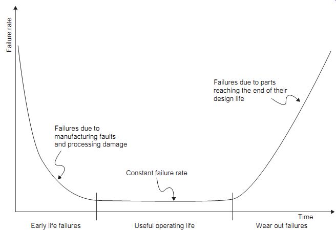
FIG. 1 The bathtub diagram
===
Bathtub diagram
The time/failure rate curve is often referred to as the bathtub diagram because of its shape. The high level of early failures shown in FIG. 1 is often described as infant mortality. These are usually due to manufacturing faults, deficiencies in the quality control scheme, design deficiencies, or mis use by or the inexperience of the end user. These failures are fairly quickly eradicated and the failure rate settles down to a constant, often zero level over the normal working lifetime. Towards the end of the useful service life, the failure rate starts to rise once more and this is described as the wearout region. Equipment may be 'burned in' by the manufacturer; that is, operated at full power and possibly elevated temperature for a defined period to reduce the possibility of infant mortality affecting the end user; this may also be done after repair, when it is usually referred to as soak testing.
Mean time between failures (MTBF) is a factor that is often quoted.
For a system with a constant failure rate of, say, 0.001 per hour, it would be expected to fail and have to be serviced every 1000 h. Thus, the average or mean time between failures would be 1000 h. MTBF is therefore the reciprocal of the constant failure rate. When it is not practicable to replace a failed component, it is more usual to refer to the mean time to failure.
Mean time to repair (MTTR) or downtime is the term used to describe the length of time that a system is out of action between failure and repair.
If components and systems are operated at below their normal design parameters, their lifetime can be extended, a technique often described as derating. In fact capacitors often fail in a system that is running at near to the upper temperature limit for the components. Increasing the rating of a capacitor from, say, 85ºC to 105ºC will improve the system reliability.
Typically, an electrolytic capacitor rated for service at 105ºC is specified to have a service life of 6000 h at 105ºC. This is just 250 days, so for most applications one would want to use it at much lower temperatures.
Even in the servicing environment, it is important to report consistent failures because this can be accumulative throughout a wide area and could lead the manufacturer to improve the design.
Surface-mounted technology
Surface-mounted technology (SMT) uses components designed to be as physically small as possible without the constraint of having to have long, stiff, wire leads attached to the component body. These small sometimes leadless components are attached by direct soldering to the metallic conductor pads on the circuit boards. One of the advantages is being smaller than their conventional counterparts, but the main advantage is that the printed circuit board (PCB) no longer requires holes for every component lead, so making the PCB both cheaper and smaller, and this leads to smaller subsystems. Because of the relatively large area of the solder joint between component termination and the solder land on the PCB, highly reliable joints are produced with good heat-dissipating properties. Usually, SMT components have lower series inductance from being physically small and not having long leads, so that these devices have better radio frequency (RF) characteristics. Surface-mounted construction is dominant in all areas of electronics, from audio to microwave systems. The technology of surface-mounted components or devices (SMCs or SMDs) is highly compatible with automated assembly, which in turn further improves the cost-effectiveness.
Most SMDs are supplied on tape and reel; typically, several thousand devices are supplied on a carrier tape, rolled on a reel much like a super 8 or 16 mm cine film reel, designed for automatic pick and place equipment.
When small quantities of components are bought they are often supplied in sealed antistatic plastic bags. They should be stored in their packaging until actually needed, to avoid mixing components that are difficult to identify. It is also a good idea to keep SMCs in airtight containers to reduce the chance of the terminals tarnishing or the plastic body of integrated circuits (ICs) and some capacitors absorbing water from the air. The protection of components from absorbing water from the atmosphere and tarnishing of the connecting terminals has become particularly important since the introduction of RoHS legislation in Europe, which banned lead from solder, resulting in higher soldering temperatures and greater risk of damage to the component. It is very important to use the correct solder for the type of component and PCB being worked on: lead-based solder such as 60/40 or the fully eutectic 63/37 will continue to be available for maintenance and repair for some years to come, and these solders must not be mixed with lead-free types, as the joint reliability would be impaired.
Most discrete SMDs are too small to mark a value on them in the conventional way, with colour or laser scribing or heat-cured ink printing.
Typically, ceramic SMD capacitors are unmarked, some resistors are marked usually with a three- or four-character code, inductors are similarly marked, transistors usually have a three-character code, and larger devices such as ICs and power transistors are marked in the normal way. The coding shown in Table 1 is commonly used.
Common resistor markings include two-, three- and four-symbol versions. Typically, the two-symbol code would be Q5 for a 390 kO resistor, while for the three-symbol code, the first two digits indicate the base figures and the third digit indicates the multiplier or number of zeros to add.
Therefore, 270 = 27R or 27 pF, 331 = 330R or 330 pF, 472 = 4.7 K or 4.7 nF.
Some manufacturers use the letter R as a decimal separator for both resistors and capacitors; for example: 2R2 = 2.2R or 2.2 pF or 2.2 µH. Four-digit codes are similar, using the first three numbers for the value and the last digit for the multiplier.
==
Table 1 SMD component marking codes.
===
Aluminum electrolytic capacitors may use a three-symbol code with numbers to indicate capacitance value in microfarads, plus a letter to indicate the voltage rating, as follows: C = 6.3 V, D = 10 V, E = 16 V, F= 25 V, G =40 V, H = 63 V.
The position of the letter in the code indicates the decimal point in the capacitance value. For example, F47 = 0.47 µF 25 V, 3E3 = 3.3 µF 16 V, 22C= 22 µF 6.3 V.
Devices such as discrete transistors and diodes are marked according to different manufacturers' systems, so it is not unusual to find two different devices with the same code. Some common examples of transistor and diode marking for common SOT23 package devices are 1F for the Philips BC847B (which is a SMD version of the BC107B/BC547B) and A6 for the BAS16 diode.
Always check the manufacturer's data sheet when identifying SMD transistors and diodes. There are too many devices with similar codes to assume anything.
Soldering technology
Allied to the use of SMDs are the changes in soldering technology that have occurred over recent years. Repair and component replacement of surface-mounted PCBs now typically require a microscope and fine tweezers, along with a temperature-controlled iron, a hot-air pencil and a very steady hand. Great advances in reliability have been made by the use of automatic processing for surface-mounted assembly; however, it has made repair and maintenance much harder. The introduction of the RoHS legislation has also affected things because there are now several incompatible lead-free solder systems in use, as well as the legacy of lead-based equipment. It remains to be seen whether the reliability of the lead-free systems approaches that of the older, lead-based solder.
The PCBs or substrates used with SMDs often have no through-holes for conventional components; the component lead-outs are soldered directly to pads or lands provided on the metal tracks. This feature required the development of new soldering and automation techniques which yield further advantages. In manufacture, the soldering methods that are used lead to improved connection reliability, which in turn leads to a reduction in costs.
The particular technique used in manufacture has a bearing on the way in which SMDs can be handled during servicing.
• Wave soldering: the components are attached to the solder resist on each PCB, using an ultraviolet light or a heat-curing adhesive. The boards are then passed, inverted, over a wave soldering bath with the adhesive holding the components in place, while each joint is soldered.
• Reflow soldering: a solder paste or cream is applied to each pad on the circuit board through a silk screen, and components are accurately positioned and held in place by the viscosity of the cream. The boards are then passed through a reflow oven or over a hot plate, to reflow the solder and make each connection.
• Vapor phase reflow soldering: this more controlled way of operating the reflow process uses the latent heat of vaporization to melt the solder cream. The boards to be soldered are immersed in an inert vapor from a saturated solution of boiling fluorocarbon liquid, used as the heating medium. Heat is distributed quickly and evenly as the vapor condenses on the cooler board and components. The fact that the soldering temperature cannot exceed the boiling point of the liquid (215ºC) is an important safety factor.
Electronic components experience distress at all elevated temperatures.
For example, in wave soldering, most baths have an absolute limit of both temperature and time; normally, 260ºC for no more than 4 s. As the dam aging effects of heat are cumulative, manufacturing and servicing temperatures have to be kept to a minimum. The common 60/40 tin/lead solder (melting point + 188ºC) and the lower melting point tin/lead alloy (fully eutectic alloy solder has a melting point of 183ºC) were widely used, along with 62.5% tin, 36.5% lead, 1% silver alloy (62.5/36.5/1 Sn/Pb/Ag), which had improved leaching and vibration performance.
Components often have silver- or gold-plated lead-outs to minimize con tact resistance. Tin/lead solder alloys cause silver leaching; that is, over a period of time the solder absorbs silver from the component and eventually causes a high-resistance joint. This can be avoided by using a silver-loaded solder alloy such as 62% tin, 35.7% lead, 2% silver and 0.3% antimony.
Such a solder has a melting point of 179ºC. Tin also tends to absorb gold with a similar effect, and this is aggravated by a higher soldering tempera ture. This latter alloy is thus particularly suitable.
The new RoHS compatible alloys are mostly similar, 95.5% tin, 3% silver, 0.7% copper, with a high melting point (217ºC). These solders should not be used with conventional non-RoHS SMDs because of the overheating risk. It is generally safer to use tin/lead solder if in doubt.
The fluxes used to clean the metal surfaces and prevent oxidation during soldering are also important. An effective flux improves the solderability of the components, the rate of solder flow and hence the speed at which an effective joint can be made. The flux used for SMD circuits should be either a halide-free no-clean compound, or one of the water-soluble types, which should be thoroughly washed away after completion of the soldering. Acid
fluxes like those used by plumbers should be avoided as their residues after soldering can corrode through the thin copper PCB traces and component terminations.
Surface-mounted device values and tolerances
Resistor values and tolerances for SMDs are the same as those used in more conventional applications. Because of the block-like structure and the good heat-dissipating properties of the lead contacts, the power dissipation may be higher than expected. Typical common ratings range from 1/10 to 1/4 W. Capacitors also have a normal range of values and tolerances, except for the non-availability of very high capacitances. The common range of values extends from a few picofarads up to several microfarads, but the working voltage ranges tend to be somewhat lower. A typical ceramic capacitor range includes 50 V parts up to 100 nF and 16 V up to 470 nF. Available capacitances for a given case size fall with a rise in working voltage.
Both resistors and capacitors are also manufactured in multiple units, typically up to eight resistors or four capacitors in a single block.
Typically, inductors are available ranging from 1 nH to 1 mH at up to 5 A of saturation current. Similarly, transformers that cover frequencies ranging from audio applications to lower microwave bands at around 6 GHz are currently in use.

FIG. 2 Typical surface-mounted IC packages: (a) 100-lead MQFP, (b)
44-lead PQFP, (c) 28-lead PLCC, (d) 20-pad LCC, (e) SO8, and (f) SOT23
Packaging
The familiar single in line (SIL) and dual in line (DIL) devices that have been used for years are now supplemented by a large number of other packaging methods, particularly for computer chips and SMDs (FIG. 2). These new packaging systems have generated new and sometimes obscure abbreviations.
These include small outline package (SOP), with variations like thin small outline package (TSOP) and thin shrink small outline package (TSSOP), which refers to a small outline package that is smaller than standard and usually has a finer pin pitch. Discrete devices also have new abbreviations: SOT for small outline transistors and SOD for small outline diodes. More recently, ICs such as op-amps and voltage regulators and low pin-count microcontrollers have begun appearing in very small outline packages (VSOPs) or leadless laminate package (LLPs) and quad flat no leads (QFNs); these are typically the same package from different vendors made from a laminated glass epoxy material with metal contacts on the underside only.
Complex ICs may be directly mounted on to a circuit board or occasion ally plugged into a socket. Large ICs with contacts arranged around four sides of a square are described as quad flat packs (QFPs) or plastic quad flat packs (PQFPs). Integrated circuits designed to be either mounted in a socket or soldered directly to the PCB use J-lead contacts and are usually described as plastic leaded chip carrier (PLCC). Ceramic versions, e.g. leadless ceramic chip carrier (LCC), are typically used in older high-rel equipment and sometimes for prototypes and production fixes.
A further development involves the use of ICs with several rows of contacts arranged around the four undersides of the square chip package, which terminate in sometimes more than 400 contact bumps. Each of these is soldered directly to matching pads on the circuit board by one of the methods described above. This ball grid array (BGA) system creates real difficulties for repair or replacement. The only way to remove the chip is to use a hot-air gun or infrared rework station and then lift off the chip once all the solder under it has melted. This needs to be done as quickly as possible to prevent damage to the surrounding components and the PCB material. For replacement purposes, pads of pre-aligned solder bumps are available in a grid format to be used when replacing BGA devices; generally, it is not economical to repair BGA boards.
Fault-finding on surface-mounted technology boards
As with discrete component circuit boards, the divide and conquer or half split technique has much to recommend itself in terms of time spent on fault-finding with SMT boards. Locating the faulty area by signal tracing is applicable to both analog and digital circuits. Once the faulty area has been located, the component or IC will have to be tested. L, C and R devices are usually fairly straightforward. Disconnect the suspect component and check the circuit board for any unexpected short- or open-circuits associated with the contact pads that might have caused the fault. Test the displaced component to determine that it is in fact faulty before replacing with a new one. Even if doubt exists that the component might be service able, remember that the heating effects of removal and refitting could lead to an early failure. It is therefore often advantageous to fit a replacement.
To test a suspect IC, measure all the d.c. voltage supply points for correct value. Check for the same voltage levels on adjacent pins and check the continuity of earth lines. If signals are present at the input, and if the IC is serviceable and not overheating, then signals should be found at the out puts. However, there are a few exceptions to this rule, where some power output stages, voltage stabilizer circuits or similar may have shut down through an excessive rise in temperature.
If an IC has failed, it is important to ascertain why before fitting a new one. Check all the supply lines for open- or short-circuits while the IC is out of circuit. Check particularly for any adjacent pins that have acquired the same voltage levels. This may be caused by a short-circuit somewhere in the circuit tracks (FIG. 3).
===
(b) Termination (Metal end cap) Multilayer ceramic capacitor (a) Laser trim cut Laser trim cut Thick film (Resistor) Termination (Metal) Ceramic substrate (c) Polarity indicator Termination Value marking Epoxy packaged tantalum capacitor 106
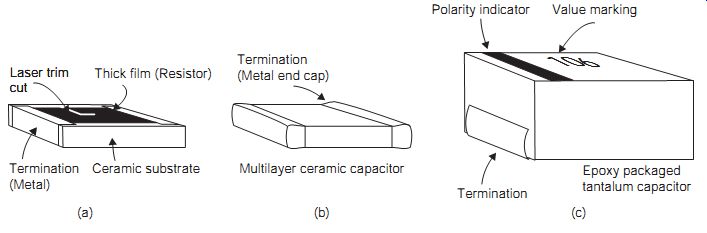
FIG. 3 Discrete SMD components: (a) thick film resistor, (b) multilayer
ceramic capacitor, and (c) tantalum capacitor
===
Servicing SMT equipment
For the larger centralized service department, a soldering rework station may be cost-effective. This may include a small portable vapor phase soldering unit, such as the Multicore Vaporette, which is particularly suited for small batch work as commonly found in such establishments. For the smaller service department, much ingenuity might be needed when dealing with SMD circuits.
The method used to remove suspect components may vary with the number of leads per device. For a device with only two or three leads, a fine soldering iron, in conjunction with a solder sucker or solder braid, can be successful. For multipin ICs, two methods are popular. One involves directly heating the soldered connections with a carefully temperature controlled hot-air jet. The other method uses an electrically heated collet or special extension to a conventional soldering iron, to heat all pins simultaneously. When the solder flows, the component can be lifted away.
In a simpler way, all the leads can be severed using a pair of cutters with strong, fine points. The tabs can then be removed separately. This is not quite so disastrous as it appears. Any suspect component that is removed, and subsequently found not to be faulty, should not be reused; the additional two heating cycles are very likely to lead to premature failure. As the desoldering of even a few leads can be difficult, it is important that the circuit board should be firmly held in a suitable clamp.
Even after all the solder has been removed, a problem of removing the component may still exist if an adhesive was used in manufacture. Although care should be exercised when prising the component off the board, damage to the printed tracks is unlikely. The adhesive should have been applied only to the solder resist. After component removal, boards should be examined under a magnifier to check for damage to the print.
For SMD work the soldering iron used should be a temperature-controlled type rating and should not be applied to a joint for longer than necessary. If solder takes much more than 3 s to melt it may be necessary to use an iron with a greater thermal capacity. It is better to use a larger iron (temperature controlled) than a small one that fails to do the job quickly. The heat from the iron should be applied to the component termination and the PCB pad simultaneously, and the solder should flow on contact with either surface, otherwise a poor joint will result. Never rely on a joint made by carrying solder to the joint on the iron, since all the flux will have been burned away and will not clean the metal surface of oxides before the solder cools, which is necessary to make a good joint.
Before starting to fit the new components, the solder pads should be lightly pretinned, using the appropriate solder and flux, but not so much as to make the surface uneven. Each component will need to be precisely positioned and firmly held in place while the first joints are made. For multi-leaded components, secure two diagonally opposite leads first. For chip resistors and similar components, first apply solder to one pad (FIG. 4a), then while heating the solder on the pad with the soldering iron to keep it molten introduce the component with tweezers (FIG. 4b). The component should be held still until the solder has solidified, then the other end of the component may be soldered in the usual way (FIG. 4c). The first joint may then need to be reworked with the addition of a small quantity of flux. The final joint should have a smooth continuous fillet (FIG. 4d, A). FIG. 4 also shows three incorrectly made joints: B is a joint with too little solder, and this produces a high-resistance connection which may also be mechanically unreliable; joint C has been made with the application of too little heat, which will also lead to a high-resistance connection; and in joint D, too much solder has been applied and this has probably resulted in excessive heating of the component.
==
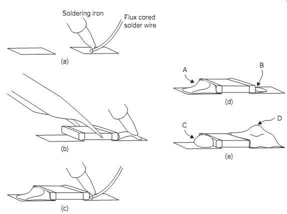
FIG. 4 Soldering chip-type SMDs: (a) apply solder to one pad, (b) melt
the solder and introduce the chip with tweezers, (c) solder the other end
once the first joint has cooled, (d) visual soldering standards, a good
joint at A and insufficient solder at B, (e) a dry insufficiently heated
joint at C and too much solder at D
===
Reliability in practice
Experience suggests that the most overstressed discrete components in a system are the capacitors, particularly the electrolytics. If these are operated at too high a temperature, the electrolyte tends to dry out or leak. In the first case, this leads to a significant reduction in capacity with the attendant loss of performance. In the latter case, the leakage can create corrosion on the circuit board to generate open circuit tracks. When replacing a capacitor it is therefore important to ensure not only that the capacitance value, voltage rating and equivalent series resistance (ESR; typically 2 x 10^-2 Ohm) are correct, but also that the temperature rating will not be exceeded. Typically, for television and satellite receiver applications, a 105ºC rating is specified, but upgrading this to 125ºC will often improve reliability. Again, if these devices are operated at too low a d.c. voltage, the dielectric material will start to decay. At first this causes the capacitance value to rise with the thinner dielectric, but this quickly punctures and becomes a short-circuit.
Modern circuit boards tend to be liberally populated with these devices and experience has shown that when one fails the others are quite likely to follow suit in quick succession.
Safety testing
It is important to point out that there are generally two earth points within electrical equipment. The primary earth ground (PEG) or protective earth is designed to provide protection against electric shock to the user, and the secondary earth ground (SEG) or signal earth is used to provide a return path for signals within the equipment. Great care needs to be exercised where the two earths are connected together within a system. Each item of electrical equipment is connected to the mains supply via a green/yellow earth cable.
Portable appliances are pieces of equipment that are powered via flexible leads plugged into a mains single-phase electrical supply of 230 V a.c.
Industrial equipment may be similarly connected to three-phase, 400 V a.c. mains, but is covered by a different class of regulation.
Within the single-phase group there are three classes of equipment, defined as follows:
• Class 1: with this equipment, the basic electrical insulation is addition ally supported by providing a connection between the exposed metal parts and the protective earth provided by the mains power supply. This technique is used in all industrial equipment.
• Class 2: with this equipment, the protection does not rely on the basic insulation, but on additional internal insulation and the avoidance of any electrical connection to any exposed metal work. These are often described as being double insulated and are suitable only for domestic applications.
• Class 3: such equipment is designed for use with safety extra-low voltage (SELV) supplies that operate at less than 25 V a.c. r.m.s. or 60 V d.c. Rechargeable battery-operated portable tools fall into this class.
All appliances connected to the mains supply via flexible leads and plug and socket connectors should be examined and tested at least annually by a competent person.
• Flexible leads should not be frayed, split, sharply kinked, cut or too tightly clamped.
• Damaged leads should be replaced immediately.
• Cables must be securely fastened at both the plug and the equipment.
• The supply cable to a heavy piece of equipment should be connected in such a way that the plug and socket will separate if the cable is pulled.
• The live end of the connector should have no exposed pins that may be touched.
• Every connection should be both mechanically and electrically sound.
• The cable must be well secured with no danger of working loose and with no stray strands of wire.
• Finally, be aware that hot soldering irons can easily damage power leads.
It is important to be able to test and record the earth bond resistance, earth loop impedance and insulation resistance between line, neutral and earth after any repairs. This will ensure that the work carried out meets the standards required by law.
Various suitable test units are available from manufacturers such as AVO, Megger Ltd and Seaward Ltd, which are readily portable and simple to use.
The old-fashioned Megger, which is still often used, uses a hand-cranked generator to provide the test voltages, with the test results being indicated on a moving-coil meter. The modern versions are driven from a mains power supply or a 9 V battery to provide the necessary high test voltages. Most test sets have at least two ranges, 0-200 M and infinity for insulation resistance and 0 to 2 O for continuity. The indication of the results is displayed on a liquid crystal display (LCD) screen, which is supported by a battery-backed semiconductor memory. The results can then be downloaded into a personal computer (PC) memory for future reference.
The continuity and resistance of the earth lead should be tested while passing a current of 25 A for 5 s, which is high enough to open-circuit a partially fractured cable. The earth bond resistance should be in the order of 0R1 and not greater than 0R5 if the appliance plug is fused at 3 A or less.
This test is carried out by inserting the appliance plug into the test set and connecting the earth test lead to its conductive casing. With this test the series resistance of the mains cable needs to be taken into consideration, but commonly this combined resistance will be less than 0R5.
The insulation resistance will require a 500 V d.c. test voltage and for an earthed appliance the live and neutral pins are shorted together and the resistance between them and the earth connection is measured. The test voltage is applied for 5 s as the insulation resistance is being measured.
Typically, this should be at least 2 M. For a double-insulated device that carries the double square symbol, the test lead is connected to any exposed metal work and the insulation resistance should be higher than 7 M.
It is also useful to attach a self-adhesive label to the device, recording a serial number, perhaps in bar code, referring to the test data. This will help to make workers in the field aware of the continuing need to maintain this standard. Portable appliance testing (PAT) testers are available that have the facility of storing the test data so that it may be downloaded into a PC data base for future recording purposes.
On occasions when it is necessary to measure the state of the electrical distribution network in, say, a small workshop, the job is only slightly more complex, but involves the following definitions.
• R1 = resistance of the phase conductor
• R2 = resistance of the protective earth conductor
• Hence, R1 + R2 = the loop resistance
• Zs = earth fault loop impedance
• Ze = the earthing impedance, external to the circuit
• Zs = Ze + R1 + R2, and generally in such an application, any stray reactance effects can be ignored.
Then proceed as follows:
1. Disconnect the network from the supply by means of the main circuit breaker.
2. Strap the phase to earth at the distribution board.
3. Test the loop and insulation resistance between phase and earth at each outlet socket.
4. Record this information.
Mains polarity
The polarity of the mains supply (not really an appropriate name because the voltage on the live line is alternately positive and negative) can be checked by using a neon lamp or probe. This device glows when in contact with a connection at a potential greater than about 100 V d.c. or a.c. Using a voltmeter referenced to earth, the live line voltage should read 230 V a.c. per phase.
Theoretically, since the neutral line is connected to earth at the nearest substation, this should read 0 V. However, small induced voltages of perhaps 10 V a.c. can usually in practice be measured between neutral and earth.
===
EXPERIMENT 1:
Using a range of mains-powered electronic test equipment (cathode ray oscilloscope, signal generator, electronic voltmeter, etc.), disconnect the equipment from the mains supply. With a suitable instrument or PAT tester measure and record the earth loop impedance, earth bond resistance and insulation resistance to earth.
===
Electromagnetic compatibility and interference
Electromagnetic compatibility (EMC) is defined as the ability of a device, piece of equipment or system to function satisfactorily in its electromagnetic environment without introducing intolerable electromagnetic interference (EMI) to any other system; at the same time, its own performance must not be impaired by interference from other sources. Such interference occurs as noise within a system and since this is considered as a destroyer of information, it is often a limiting factor in a communications system.
Interference can be divided into two categories, natural and artificial.
The former often results in electrostatic discharge (ESD), while the latter usually results in power-line surges. Natural sources of interference include ionospheric storms and lightning. Artificial interference commonly results from high current switching operations and RF generators. With the expansion in the use of portable digital communications systems such as computers and cordless mobile telephones, sources of interference are growing rapidly.
A direct lightning strike is not necessary to cause havoc with a communications system. Even cloud-to-cloud discharges can easily set up high electric fields that can influence power lines and overhead telephone lines, which tend to act as aerials. Instances have been recorded of induced voltage spikes in the order of about 2000 V, but of very short duration, being developed on the normal 230 V a.c. supply mains. Even if exposures to such discharges do not prove to be immediately destructive, they can intro duce a latency failure mechanism because these effects are cumulative.
The rubbing action between dissimilar materials has long been a recognized phenomenon, now referred to as tribo-electricity. A triboelectric series lists the materials ranging from air, hands, asbestos, at the most positive, through the metals, to silicon and Teflon as the most negative. The further apart in this table, the higher will be the electric charge between the two materials when rubbed together. Even the action of a person walking across a carpet or even sitting in a chair can generate very high electrostatic charges, depending on the clothing worn and level of humidity. Owing to relationship between charge and voltage (Q _ CV joules), the action of a sitting person lifting their feet off the ground reduces the body capacitance and this automatically causes an increase in the voltage level to increase the risk of ESD.
Electromagnetic interference can enter communications equipment either by direct radiation or by conduction. The effects of the former can be reduced by screening or shielding, while reduction of the latter requires the use of suitable filters.
Connecting leads, particularly the longer ones, make very good aerials for propagating interference problems. Such leads are also susceptible to breaking, where they can vibrate. The loose ends then become the source of arcing or even short-circuit problems. Such leads should therefore be dressed close to the circuit boards or chassis and firmly clamped so that their capacitive pickup effect is minimized.
Mains plug filters that have a low pass characteristic, with inbuilt shunts to discharge any excessive voltage spikes to earth, are very useful for restricting the ingress of mains-borne interference, particularly in respect to digital and computing equipment. Protection for such equipment can avoid the blackout of services which lead to complete loss of system functions.
Brownout is the jargon term used to describe partial loss of processed data.
• Holes in metalwork should have dimensions that are less than about one tenth of a wavelength at the major operating frequency. A slot is a particular form of aerial that will radiate and accept signals very effectively at higher frequencies.
• All plug and socket type connectors should maintain good low-resistance contacts, because high resistance generates heat and the resistance itself then creates a noise component.
• Shielding problems can arise after servicing by failure to replace all the screws and screen fixings correctly. Because of the wavelength effect, even the spaces between the screen-securing screws can be critical in very high-frequency equipment.
The design of connections in equipment and the connections between equipment can have a big influence on how well systems operate in a noisy electromagnetic environment. One of the most common problems with equipment is incorrect grounding, causing unwanted feedback between stages and injection of signals into input stages and intermediate stages.
FIG. 5 shows how badly designed grounding can lead to problems.
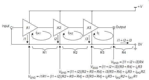
FIG. 5 How incorrect grounding can lead to ground voltages other
than 0 V
Since all three stages of the amplifier share the wire that provides the ground return for the power supply and the signal, voltages will be developed across the resistance that this wire presents to the currents. These will range from d.c. values for the power supply current for each stage to a.c. signals which are of varying phase. These will all add to make an error voltage at the ground connection of the stage, which can result in feedback effects and d.c. offsets, resulting in erroneous output signals, instability or distortion. The problem can be cured by reducing the resistance of the earth tracks to a very low level; in high-frequency circuits this is often seen as a continuous ground plane on one or other side of a PCB or sometimes as a buried layer. The effect is even more pronounced at very high frequencies when the circuit operation can be improved by the addition of individual stage screening.
FIG. 6 shows another useful approach called star point grounding. This is particularly appropriate where an output stage may have significantly higher current drain than other stages, and is often used in audio amplifiers, etc.
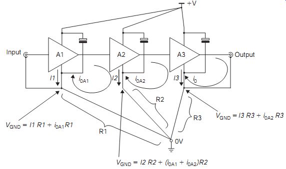
FIG. 6 Improved circuit performance through the use of star topology
for ground and supply.
Another grounding effect is earth loops between equipment. This may be seen on the test bench if an oscilloscope and a power supply without an isolated output are used to test an amplifier circuit. The power supply and the oscilloscope both provide paths to mains earth from the circuit under test, and this loop can result in quite large signals being impressed on the circuit under test, resulting in unexpected or apparently random effects. The use of a double-insulated mains power supply is common in audio equipment as it avoids the hum resulting from loops returning to mains earth.
CE marking and the Low-Voltage Directive
The UK is bound by regulations developed in the EU; these include the EMC Directive and the Low-Voltage Directive (LVD) and various other directives like the Radio and Telecommunications Terminal Equipment (RTTE), Restrictions of Substances Hazardous to Health (RoHS) and Waste Electrical and Electronic Equipment (WEEE). Each of these directives is a very complex document and their implications are closely allied in their relationship to the electronics and electrical manufacturing and servicing industries. The CE marking signifies that the product or equipment to which it refers meets all the requirements of all relevant EU harmonized directives, including the health and safety features, complies with the appropriate regulations of LVD EN60950 and meets the emissions and immunity of EN50081/2.
Even the relative dimensions of the two circles that form the basis of the CE marker characters are specified (FIG. 7): the characters of the mark must be at least 5 mm high.
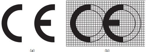
FIG. 7 (a) CE mark applied to equipment indicating that it meets
all the requirements of all relevant EU harmonized directives, and (b)
the specification for the CE mark shape
The standards have to be maintained throughout the product or equipment's lifetime, and also apply to second users and repaired items.
This is why the requirements have to be observed in the course of servicing.
The LVD applies to items rated at between 50 and 1000 V a.c., and 75 and 1500 V d.c. It therefore applies to all domestic entertainment equipment and most of the industrial equipment so powered.
The EN60950 directive, which applies to information technology (IT) systems and any equipment that may be connected to an IT system, is a lengthy document that chiefly relates to matters of safety, including flammability, for users, operators and service personnel. In the interests of brevity, only the most important features of the directive can be included here. For specific information the reader is referred to Further reading list at the end of this section.
All equipment is assumed to be in continuous operation unless otherwise stated on the rating label. Virtually all IT equipment is covered by this legislation, including class 1, 2 and 3 devices with pluggable connectors, plus fixed, portable and handheld equipment.
The maximum earth leakage current is 3.5 mA, which should be the trip setting of any associated earth leakage circuit breakers (ELCBs). Even lithium batteries commonly used for memory backup are specifically mentioned in the text, because these can be explosive if they are incorrectly replaced. During servicing, care must be exercised because equipment such as cathode-ray tube monitors, some laser printers and photocopiers can include extra high voltages that exceed the LVD levels.
The LVD ratings are not intended for use in the following cases, which are covered by other international specialist safety provisions:
• in ships, aircraft, railways, explosive atmospheres, radiological and medical applications
• in domestic plugs and sockets and electricity supply meters
• in electric fence controllers and parts for goods and passenger lifts.
In addition, the directive does not necessarily apply to electrical equipment intended for export to non-EU countries; although many countries have adopted the EU rules as the basis of their own legislation, some have even tighter regulatory regimes.
The CE marking is the only marking that may be used to certify that a manufactured product conforms to the standards incorporated in the relevant directives. It is a criminal offence not to mark a product that is covered by LVD or so mark a product that does not comply.
Equipment may be provided on the market only if, having been constructed in accordance with good engineering practice in the safety matters in force within the community, it does not endanger the safety of persons, domestic animals or property when properly installed, maintained and used in the applications for which it was intended.
Third party conformity assessment is normally carried out by a recognized test house. These organizations, which can prove their conformity with the EN45000 series standards, which cover the criteria for the operation and standards testing of new equipment, are designated by the member states.
These bodies may submit an accreditation certificate together with other documentary evidence. Under this system, the manufacturer takes full responsibility for the assessment, testing, documentation and declaration of conformity and the CE marking. A technical file (see below) or documentation must also be available on demand for the national enforcement authorities.
The RTTE directive covers devices such as mobile phones, wireless and wired networking equipment, remote keyless entry devices that use radio signals, CB and PMR equipment, and domestic radio and television receivers. The directive sets up a harmonized European framework of frequency bands and power limits with the aim of allowing the free movement of goods while preventing interference to services.
The RoHS directive sets requirements on the chemical composition of the materials used in the manufacture of equipment, and focuses on the materials that are embodied in the equipment or discharged into the environment as a result of manufacture. This and the associated WEEE directive, which defines how equipment must be dealt with at the end of its useful life, are intended to control the normal processes and products of manufacturing.
To certify conformity with the directives and the CE marking, the manufacturer must draw up a technical construction file covering the design, manufacture and operation of the equipment, prepare an EC declaration of conformity and affix the CE marking.
Control of Substances Harmful to Health
Control of Substances Harmful to Health (CoSHH) deals with the safe use of chemicals and other materials, and accidents involving them.
The human effects of hazardous substances require specialist treatment and it is therefore important that first aiders should be chemically aware of the associated problems. Under the regulations, all harmful substances should be stored in a cool, dry place and used with safety concerns as the primary consideration. The person responsible for this store should also be a trained chemical first aider. The safety information provided by the manufacturer should be stored where it is readily accessible to the appropriate member of staff, who may need it in a hurry.
Common solvents such as trichloroethane, trichloroethylene and carbon tetrachloride (CTC) that have in the past been used for cleaning and degreasing are now banned under EU law. Because all chlorinated solvents have narcotic and anesthetic properties, any such solvents that are still in use should be treated very carefully. (Chloroform, another member of the family, is a well-known anesthetic.) High levels of exposure to this group of substances can lead to kidney and liver damage. Of the group, only trichloroethane is non-carcinogenic. Although these substances are non-flammable, when chlorinated fluids are exposed to heat, they liberate the chemical warfare gases known as phosgene and hydrogen chloride. The chlorinated solvents can enter the human body either by inhalation or by skin absorption.
The use of chlorofluorocarbons (CFCs) is progressively being phased out, largely because they are destroyers of the upper atmospheric ozone layer, which protects against ultraviolet radiation from the sun. Apart from refrigeration applications, CFCs have been used as degreasing agents and freezer sprays. The very low boiling point can create frostbite owing to rapid evaporation and can strip the fatty tissue from the surface of human skin. Therefore, great care needs to taken when using up old stocks of CFCs.
Hydrochlorofluorocarbons (HCFCs), which are being used as temporary replacements for CFCs, are very good and non-destructive cleaners, and are non-flammable. However, under extreme heat they break down to generate phosgene, hydrochloride and hydrogen fluoride gases, so need to be very carefully stored.
Ethyl alcohol or ethanol, and its relative methylated spirits, are very good cleaning agents but are highly flammable and highly toxic, and can cause liver damage if drunk. This group also absorbs water fairly easily and this slows down the evaporation process.
Isopropyl alcohol (IPA), which is highly flammable, is a relatively safe cleaning agent, although its near neighbor, N-propanol, is classified as toxic.
Petrol and benzene are both extremely good degreasing and cleaning agents, but are highly flammable and explosive. They are harmful to health via skin absorption and the respiratory system and are also carcinogenic.
White spirit, which is commonly associated with paints, is highly flammable and produces narcotic fumes, which are harmful if they enter the respiratory system.
Solvents such as xylene and toluene, which are constituents of some switch cleaners and adhesives, produce euphoria (the glue-sniffing syndrome) and lead to serious problems such as respiratory failure and death, damage to the central nervous system and liver damage through skin absorption. Acetone and amyl acetate are solvents that produce toxic fumes and are also a fire hazard.
Many of the adhesives and sealants used in the servicing environment are also likely to create health risks when used at elevated temperatures. Long periods of exposure to the fumes from epoxy resins (two-part mixes) can also be a source of liver problems. While silver loaded epoxy glues have a low resistance that makes them useful for re-fixing metal shields within a piece of electronic equipment, the period of exposure can be reduced by raising the temperature to about 40-50ºC to cut the curing time in half.
Solder fluxes (rosin or colophony) produce fumes when heated that can cause industrial asthma. Since the low-fume alternatives are also suspect, it is most important that all soldering operations are as far as possible carried out under a fume extractor hood. Fume extractor kits that mount directly onto a soldering iron are available, but tend to make the work more difficult. Smoke extractor hoods incorporate a charcoal filter that needs to be replaced periodically. The fumes from the lead in solder are also problematical, but while a smoke hood is helpful, the use of lead is included in regulations that are not within the scope of COSHH.
As with all accidents, events that are covered by COSHH must also be recorded in the workshop accident books, which must be kept up to date by a responsible person and be available for inspection by the appropriate authority.
The EU directives referred to in this section cover several weighty volumes and are written in legalistic terms. The information presented above can only represent a brief summary of the salient points in each document.
For further and more explicit explanations of the directives, the reader can usefully refer to the publications listed below.
QUIZ:
1. What defines a customer's view of product quality ?
(a) quality control testing
(b) design
(c) fitness for purpose
(d) cost.
2. When does 'infant mortality' affect products?
(a) at the beginning of service life
(b) during manufacture
(c) after burn-in
(d) when they are of low quality.
3 A surface-mounted electrolytic capacitor marked 5E6 has a resistor marked W5 connected in parallel with it. What are their values?
(a) 56 µF 25 V and 68 kO
(b) 56 µF 16 V and 68 kO
(c) 5.6 µF 16 V and 680 kO
(d) 0.56 µF 6.3 V and 680 kO.
4. What should you use to solder a surface mounted component to a PCB?
(a) a low-power soldering iron
(b) a temperature-controlled iron with enough power to do the job quickly
(c) an acid flux
(d) a method that does not heat the component.
5. What is significance of the CE mark on a piece of electrical equipment?
(a) it was made in Europe
(b) it meets the LVD and EMC directives
(c) it complies with all relevant EU directives at the time of manufacture
(d) it was designed in Europe.