AMAZON multi-meters discounts AMAZON oscilloscope discounts
PART 3
Goals:
1. Demonstrate an understanding of power supplies, to component level
2. Demonstrate an understanding of amplifiers, to component level and apply this knowledge safely in a practical situation
3. Demonstrate an understanding of oscillators, multivibrators and waveform generator circuits, to component level.
Direct current power supplies
Direct current ( d.c.) power supplies are required by most electronic systems, either powered from the alternating current (a.c.) mains supply or operating from batteries. The purpose of the power supply circuit is to provide a constant voltage or in some cases current with minimum ripple and other disturbances to the system. A supply may have to respond quickly to changes in the current demanded by the circuit without allowing the supply voltage to exceed the specified operating limits. The majority of d.c. power supply circuits are ultimately supplied from the mains a.c. supply, so one of the most important functions of the supply is to convert the a.c. into d.c., usually using diode rectifier circuits.
In all rectifier circuits (FIG. 1) each diode will be reverse biased for half of the a.c. cycle and conducting for the other half. The amount of this reverse bias depends on the type of circuit used, and is greatest for a half wave rectifier feeding into a reservoir capacitor.
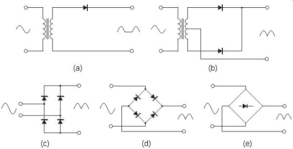
FIG. 1 Rectifier circuits: (a) half-wave, (b) full-wave centre tapped,
(c) bridge rectifier, (d) alternative drawing, and (e) symbol for bridge
rectifier
===
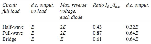
Table 1 Rectifier circuits compared for peak input
===
Table 1 shows the operating results that may be expected from rectifiers of the three types described, half-wave, full-wave and bridge, given an a.c. input of E V peak (0.7E V r.m.s.) and smoothing by a reservoir capacitor of adequate size. Note the large difference between no-load output voltage and the fully loaded voltage.
Note that in all rectifier circuits, reversing the connections of the diodes reverses the polarity of the output voltage.
===
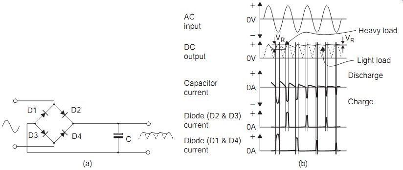
FIG. 2 (a) Bridge rectifier with capacitor, and (b) waveforms at
various loads
===
Diode current and reservoir capacitors
FIG. 2(a) shows a bridge rectifier with a capacitor connected across its output. The current flowing into and out of the capacitor (FIG. 2b) is determined by the size of the load and the size of the capacitor. Note that it is very important not to use a capacitor that is too big because a very large capacitor draws a very large ripple current; this is why packaged diode bridge circuits usually specify the maximum capacitance in the data sheet.
The simplest power supply circuits consist only of rectifiers and smoothing capacitors. In these circuits, the reservoir capacitor supplies the current to the load during the time when the diodes are cut off, and any ripple on the supply is reduced by filtering. Such circuits are adequate for many purposes, but they are too poorly regulated for use in circuits intended for measurement, computing, broadcasting or process control.
The regulation of a circuit is the term used to express the change of output voltage caused either by a change in the a.c. supply voltage or by a change in the output load current. A well-regulated supply will have an out put voltage whose value is almost constant; the output voltage of a poorly regulated supply will change considerably when either the a.c. input voltage or the output current changes. Table 1 shows how the voltage of a smoothed supply changes from the no-load to maximum-load condition.
The change in output voltage caused by changes in the a.c. supply voltage is usually less great. A 10% change in the a.c. supply will also change the output voltage of a simple power supply by about 10%, the two percent age changes being almost identical.
Example: What will be the change in an unregulated 10 V supply when the a.c. supply voltage changes from 240 V to 220 V?
Solution: The a.c. voltage change is 20 V down on 240. The percentage change is therefore 20/240 x 100 = 8.3%. Since 8.3% of 10 V is 0.83 V, the 10 V supply will drop to 10 0 - 0.83 V = 9.17 V.
===
FIG. 3 Load line of a supply: internal resistance of the supply causes
the output voltage drop as the load current is increased
===
The effect of changes in the load current (which are themselves caused by changes in the load resistance) is more complicated, because there are two main causes (FIG. 3). The first is the resistances of the rectifiers, the transformer windings and any inductors that may be used in filter circuits, and the internal resistance of the power supply. By Ohm's law, a change in current flow through such resistances must cause a drop in the output voltage.
The second effect is the voltage drop that takes place across the reservoir capacitor as more current is drawn from it. This voltage drop (V) can be quantified approximately by using the equation:
V=It/C
where I is the load current (amps), t is the time (seconds) elapsing between one charge from the reservoir and the next, and C is the capacitance of the reservoir (farads).
Solution: In a full-wave rectifying circuit, the time between peaks is 10 ms.
Substituting the data in the equation gives:
A 50 V supply, for example, would give an output which drops to 41 V between peaks, and a 9 V peak-to-peak ripple at 100 Hz would be present.
Regulator circuits
A regulator circuit connected to a rectifier/reservoir unit ensures that the output voltage is steady for all designed values of load current or of a.c. supply voltage. Such a circuit can only do its job, however, if the rectifier/ reservoir unit is capable of supplying the required output voltage (measured from the minimum of the ripple wave) under the worst possible conditions, when a.c. supply voltage is minimum and load current is maximum.
The regulator will then prevent the output voltage from rising above this set value even when load current is small or the a.c. supply voltage is high.
A regulator requires a reference voltage that remains steady, and the action of the regulator is to compare the output voltage to this reference voltage and adjust the output accordingly. The reference voltage is obtained from a Zener diode.
===
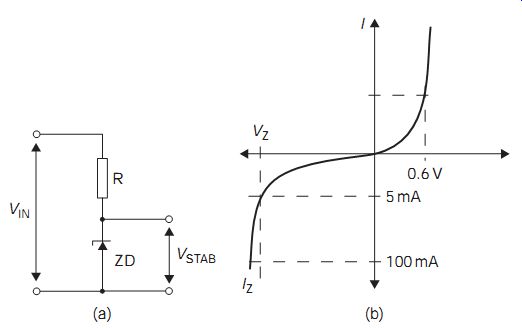
FIG. 4 (a) Simple Zener diode shunt regulator, and (b) the Zener
diode I/V characteristic curve
===
Zener diode regulation
A Zener diode is used reverse biased so that the junction breaks down to permit current flow through the diode. This breakdown occurs at a precise voltage whose value depends on the construction of the diode, and causes no damage provided the current flow is not excessive. To prevent this, current must be regulated by connecting a resistor in series with the diode. The output of a Zener diode circuit is therefore a regulated voltage.
A simple regulator circuit is shown in FIG. 4, with the output voltage across the diode being used to supply any other circuit or part of a circuit that requires a stable voltage. Many circuits, especially measuring and oscillator circuits, are adversely affected by voltage variation, which can be caused by changes in the supply voltage or changes in the current drawn by the load.
Open-circuit diode failures have the following effects:
• The d.c. output of rectifier circuits either is reduced or falls to zero.
A half-wave circuit will have no output; full-wave and bridge circuits will have reduced output, with ripple at supply frequency if only one diode fails.
• A Zener diode regulator will give a higher voltage output, without regulation.
Short-circuit failures of diodes have the following effects:
• Rectifier circuits will blow fuses, and electrolytic capacitors may be damaged. A short-circuit diode will usually fuse itself, so becoming open-circuit. In a bridge circuit, a short-circuit diode will usually cause another diode to become open-circuit.
• A Zener diode regulator will give zero output.
Two basic types of regulator are used, a series circuit and a shunt circuit.
The simplest example of the shunt type is a Zener diode regulator, illustrated earlier. In this type of circuit, the amount of current drawn from the power supply is constant. When load current is maximum, the regulator circuit current is minimum. When the load takes its minimum current, the regulator circuit takes its maximum current. The arrangement is therefore such that load current plus regulator current is always a constant value. The constant current flowing through R produces a constant voltage drop across it. So, if the input voltage remains unchanged, the output voltage will also remain constant.
The maximum dissipation of the Zener diode in this circuit is given by:
Zener voltage x Maximum current
... with dissipation in milliwatts if the current is measured in milliamps.
The maximum dissipation of the resistor is given by:
(Unregulated voltage - Zener voltage) x Maximum current
===
Example:
A 5.6 V (5V6) Zener diode is used to supply a load which takes a maximum current of 15 mA. If the minimum desirable Zener current is 2 mA, and the unregulated voltage is 12 V, find (a) the value of series resistance that must be used, (b) the maximum Zener dissipation, and (c) the maximum dissipation in the resistor.
===
Solution:
With 15 mA flowing through the load and 2 mA through the Zener diode, total current is 17 mA. The voltage across the resistor is 12 - 5.6 = 6.4 V, so that (a) the required resistance value, using Ohm's law, is 6.4/17 = 0.376 K or 376 ohms. In practice, a 330 ohm resistor would be used, making the total current 6.4/.330 mA _ 19.4 mA. (b) At a current of 19.4 mA, the dissipation in the Zener diode is 5.6 x 19.4= 108.6 mW, and (c) the dissipation in the resistor is 6.4 x 19.4 =124.2 mW.
The shunt regulator is limited in its use by being inefficient and not good at regulating over a wide range of output currents. Usually, a better way of regulating the output of a power supply is by means of a series regulator in which a transistor is connected between the supply and the load (FIG. 5). This is a much more common type of regulator circuit.
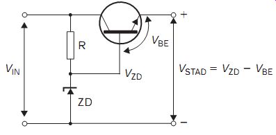
FIG. 5 Basic series regulator circuit, sometimes called an amplified
Zener regulator
When this type of regulator circuit is used, the transistor takes only as much current as the load, unlike the shunt regulator which takes its maximum current just as the load takes minimum current. The base voltage of the transistor is held constant by the regulator action of ZD1 and R1. The emitter voltage, and so the conduction, of transistor depends on the load voltage. If the demand for load current increases, the output voltage will tend to fall, increasing the forward bias. This allows it to pass more current to meet the demand. If the requirement for load current falls, this effect will be reversed.
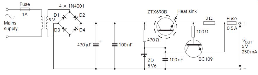
FIG. 6 Mains power supply with output current limiter and Zener diode-based
series regulator
The power supply in Figure 33.6 includes output overcurrent protection with the conventional series regulator circuit, this protects the regula
tor from possible overheating and the powered equipment from the effects
of overcurrent under fault conditions. In operation the output current
flows through the 2 O resistor in series with the 0.5 A fuse. If the output
current reaches about 0.3 A the voltage drop across the 2 O resistor begins
to turn on the BC109 transistor, which 'steals' base current from the series
pass transistor, reducing the output voltage and therefore the output current.
This is usually described as soft limiting or foldback limiting.
++++++++
Experiment 1
Make up a simple series regulator circuit with the following compon ent
values: R=330R, ZD = 5V6 and a 2N3055 transistor. Vin = 10 V. Connect
this circuit to the power supply used previously, and draw a set of regulation
curves for the stabilized circuit. Measure also the ripple voltage at maximum
load current: (a) across the reservoir capacitor, and (b) across the load.
++++++++++++++++
More elaborate series regulator circuits use integrated circuit (IC) comparator amplifiers to drive the series transistor, and the whole circuit is in IC form. The use of IC regulators has now almost totally replaced discrete regulator circuits.
Integrated circuit regulators
Integrated circuit regulators are available in a wide variety of types, each tailored to specific circuit requirements, but the simplest are the familiar fixed voltage types such as the 7805. The final two digits of this type number indicate the stabilized output, 5 V for this example. The 7805 is a three-pin regulator which requires a minimum voltage input of 7.5 V to sustain regulation, with an absolute maximum input voltage of 35 V. The maximum load current is 1 A and the regulation against input changes is typically 3-7 mV for a variation of input between 7.1 and 25 V. The regulation against load changes is in the order of 10 mV for a change between 5 mA and 1.5 A load current.
The noise voltage in the band from 10 Hz to 100 kHz is 40-50 µV, and the ripple rejection is around 70 dB. Maximum junction temperature is 125ºC, and the thermal resistance from junction to case is 5ºC/W.
The 78xx type of regulator is used extensively for power supplies in both linear and digital equipment A typical recommended circuit is shown in FIG. 6, along with the diode bridge and reservoir capacitor. The capacitors that are shown connected each side of the IC are very important for suppressing oscillations and must not be omitted. In particular, the 100 nF capacitor at the input must be wired across the shortest possible path at the pins of the IC. Some types of regulator IC should not be operated without a load, since this can cause the circuit to oscillate at a high frequency. Often, a light-emitting diode (LED) and series resistor connected at the output to indicate that power is on will be sufficient to prevent oscillation.
The maximum allowable dissipation is 20 W, assuming an infinite heat sink, and the actual dissipation capabilities are determined by the amount of heat-sinking that is used. If no heat sink is used, the thermal resistance of the 7805 is about 50ºC/W, and for a maximum junction temperature of 150ºC this gives an absolute limit of about 2.5 W, which would allow only 2.5 V across the IC at full rated current, an amount only just above the absolute minimum voltage drop.
The thermal resistance, junction to case, is 4ºC/W, and for most purposes, the IC would be mounted on to a 4ºC/W heat sink, making the total thermal resistance 8ºC/W. This would permit a dissipation of about 15.6 W, which allows up to 15 V or so to be across the IC at the rated 1 A current.
This is very useful, since a 5 V supply will generally be provided from a 9 V transformer winding whose peak voltage is 12.6 V, making it impossible to cause overdissipation at the rated 1 A current, since the voltage output from the reservoir capacitor will be well below 12.6 V when 1 A is being drawn.
It is important to be careful when specifying a transformer not to over specify the output current, because the load line of a correctly rated transformer can be used to advantage in limiting the regulator dissipation.
The 78 series of regulators are complemented by the 79 series, which are intended for stabilization of negative voltages. The circuits that can be used are identical apart from the polarity of diodes and electrolytic capacitors, and the range of currents is substantially the same as for the 78 series.
If the regulated current that is required is greater than can be supplied from any available IC regulator, then the main options are either to use a regulator to control one or more power transistors rated to pass the required current, or to use a switched mode power supply (SMPS) circuit (see later), rather than a linear regulator.
In the early days of IC regulators, the failure rate of regulator chips was very high, but later versions have added protective circuitry, which has almost eliminated failures of the type that caused so many problems at one time. The main protective measures are for thermal protection and fold back overload protection, and the effect in each case is that the output from the regulator will drop to a level that reduces risk to the regulator or to the equipment fed by it.
===
Experiment 2
Construct an IC regulator circuit, as illustrated in FIG. 7, using the 7805. Measure the output for input voltage levels that range from 6 to 12 V, and with load from 10 ohms to 1 K.
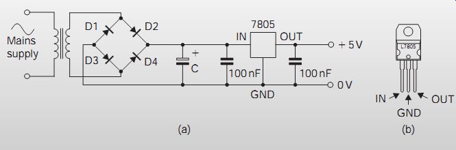
FIG. 7 (a) Power supply circuit
using the 7805 regulator, and (b) pin connections of the 7805 regulator
IC
===
The dropout of a regulator is the minimum voltage difference that must exist between input and output to sustain the action of the regulator. The dropout for the 78 series of regulator ICs is at least 2 V, and for some purposes, particularly for stabilizing supplies that are based on secondary batteries, this differential is too large. Low dropout regulators allow much lower levels of input voltage, typically down to 5.79 V for a 5 V output regulator.
Low-dropout regulators were originally developed for the car industry to provide stabilized outputs for microprocessor circuitry, and they would not be used for general-purpose stabilization for mains-powered supplies. Most low-dropout regulators feature additional protection against supply reversal, the effects of using jumper leads between batteries, and large voltage transients. Several types also feature inhibit pins, which allow the regulator to be switched back on again after it has been switched off by an overload.
Failure in discrete regulator circuits is usually caused by excessive dissipation in the main transistor, shunt or series. In the series circuit the overdissipation will have been caused by an excessive load current, unless the regulator is protected against short-circuits.
An open-circuit Zener diode will cause a shunt regulator to cease con ducting. Its effect on the series circuit is the opposite, in that the output voltage will rise to the level of the unregulated supply. A short-circuit Zener diode will cause the shunt circuit to pass excessive current. It will cause the series circuit to cut off.
Note carefully that all power transistors used in regulator circuits must be bolted to heat sinks of adequate size. Failure of IC regulators is usually due to thermal overload of regulators that do not have protection circuitry.
There are a few circuits that call for a high-voltage, low-current supply in which poor regulation is acceptable. Rather than wind a transformer especially to provide the high voltage, a voltage multiplier circuit (of which the voltage doubler is the simplest example) is often used instead. On the negative-going half of the voltage cycle shown in FIG. 8 (left), C1 is charged by current through D1, so that point X is at a d.c. voltage equal to the peak voltage of the a.c. wave.
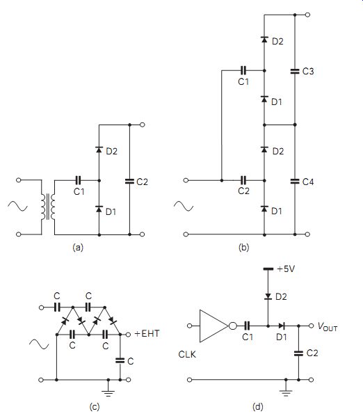
FIG. 8 (a) Simple voltage doubler, (b) quadrupler, (c) Cockcroft-
Walton multiplier, and (d) CMOS charge pump circuit
At the peak of the positive-going half-cycle, the peak inverse voltage across D1 is equal to twice the peak voltage (the previous peak charge, plus the peak a.c. value). This causes C2 to charge through D2 to the same level.
At line (supply) frequencies, the capacitor C1 must be of large value, and must be rated at the full d.c. voltage. At higher frequencies, smaller values of capacitance can be used.
Multiplier circuits of this type are commonly used to supply the high voltages required by the colour tubes in color television receivers. The circuit shown in FIG. 8(b) is effectively two voltage doublers connected in series, while FIG. 8(c) shows the Cockcroft-Walton multiplier circuit, named after its inventors. Circuits such as these are commonly used to obtain voltages as high as 25 kV for the final anode electrode of a colour cathode-ray tube. The complementary metal-oxide semiconductor (CMOS) gate-driven diode charge pump in FIG. 8(d) operates on the same principles. This circuit is often used in battery equipment where a low current voltage outside the normal rails is required: think about how it can be made to generate a negative voltage from the positive rail.
Power supply unit components
The components used in power supplies must be adequately rated for the voltage and current levels that will be used. Electrolytic capacitors can be used for low-voltage smoothing applications, but they should not be used for high-voltage supplies, particularly above 500 V. For such applications, plastic dielectric capacitors must be used and for some specialized applications, oil-filled paper capacitors. Resistors are subject to a maximum voltage rating, often 350 V or less, and where higher voltages are used, chains of resistors connected in series must be used to keep the voltage drop across each individual resistor within the limit.
Power supplies that operate at low voltages usually deliver large currents, and computer power supplies in particular will supply 20 A or more at _5 V. Electrolytic capacitors used for smoothing such supplies must be rated to have low equivalent series resistance and be able to withstand high ripple currents. Some supplies make use of a series resistor for monitoring current, and this resistor will have a very low resistance value and is typically a special purpose type.
The use of switch mode circuits allows plastic dielectric capacitors to be used in smoothing circuits rather than electrolytics, because the ripple frequency is much higher.
Switch mode power supplies
The common configuration of linear-regulated power supply consists of a mains frequency transformer and rectifier, together with an IC series regulator. The latter simply behaves as a controlled series resistance to stabilize the output voltage. Such systems suffer from several serious disadvantages:
• They are most inefficient. It is unusual to find that more than 35% of the input energy reaches the load. The remainder is dissipated as heat. The inefficiency is greater for low-voltage, high-current supplies.
• The mains transformer is invariably large. Its size tends to be inversely proportional to the operating frequency.
• The reservoir and smoothing capacitors need to be large to keep the ripple amplitude within acceptable bounds. This is particularly difficult for low-voltage supplies.
• Because the series transistor (or transistors) is operated in the linear mode it must be mounted on a large heat sink.
If the operating frequency can be increased significantly, both the trans former and the filter capacitors can be reduced in size. If the series transistor can be operated either cut-off or saturated, its dissipation will be greatly reduced. The power supply can then be made more efficient. Such operation can be achieved using an SMPS. These circuits can operate with efficiencies as high as 85%.
The basic switching principle of the most common type of SMPS (some times called a Buck converter) is shown in FIG. 9(a). When the switch is closed, current flows through the inductor or choke L to power the load and charge the capacitor C. When the switch is opened, the magnetic field that has been built up around L now collapses and induces an electromotive force (emf) into itself to keep the current flowing, but now through the flywheel or freewheel diode, D. The voltage across C now starts to fall as the load continues to draw current. If the switch is closed again the capacitor recharges. This switching cycle produces a high-frequency supply voltage.
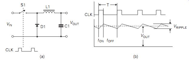
FIG. 9 (a) Basic principle of an SMPS, and (b) switching waveforms
===
Mains input
Input rectifier Input filter PWM switch HF rectifier Output filter Current limiter
Load Voltage reference Isolation barrier Opto isolator PWM controller Input protection Low voltage Mains voltage
HF transformer FIG. 10 Simplified block diagram of switched mode power supply typical of the type that powers a PC
===
The duty cycle or switching sequence is shown in FIG. 9(b) together with the output voltage Vout, that it produces. Increasing the on-period will increase Vout, whose average level is given by Vin _ ton/T. Vout can be regulated by varying the mark-to-space ratio of the switching period, with any ripple being removed by a low-pass filter in the usual way.
The typical SMPS whose block diagram is shown in FIG. 10 consists of a mains rectifier with simple smoothing whose d.c. output is chopped or switched at a high frequency, using a transistor as the switch.
For television applications this switch is commonly driven at the line frequency of 15.625 kHz. The circuit generally needs some startup arrangement that will ensure drive to the PWM switch when no d.c. output exists.
For industrial applications or computer power supplies the switching frequency is usually in the order of 20-25 kHz. The chopped waveform is applied to the primary circuit of a high-frequency transformer that uses a ferrite core for high efficiency. The signal voltage at the secondary is rectified and filtered to give the required d.c. output. This output is sensed by a control section that compares it with a reference voltage to produce a correction signal, which is used in turn to change the mark-to-space ratio of the switching circuit to compensate for any variation in output voltage. This action is effectively pulse-width modulation.
The ripple frequency of 50 Hz at the input has been changed to a frequency of 20 kHz at the output so that the smoothing and filter capacitors can be reduced in value by the ratio 20 000:50, equal to 400 times. No electrolytic capacitors need to be used.
The oscillator/rectifier part of the circuit can be operated from a battery or any other d.c. input, so that it becomes a device for converting d.c. from a high voltage to one at a lower level. Another option is to use a transformer whose input is the chopped high-frequency voltage, with several outputs that are rectified to produce d.c. at different voltage levels. Only one of these levels can be sampled to provide control, so that only one output is stabilized against load fluctuations, although all are stabilized against input fluctuations.
Switched mode power supply circuits are universal in small computers, because of the need to regulate a low-voltage supply at a high current. The usual circuitry rectifies the mains voltage directly (using no input trans former) so that the early stages operate at high voltage and low current, and a conventionally regulated supply is used to operate the control stages, ensuring that these are working at startup. A transformer for the high frequency voltage provides for isolation from the mains and for voltage output of _5 V (main output at high current), along with -5 V, +12 V and -12 V. A complete SMPS circuit can be obtained in IC form, and for higher outputs an IC can be used to control a high-power switching transistor.
The SMPS generates more radiated and line conducted noise than a linear supply. This can be reduced to acceptable levels by using:
• mains input filters balanced to earth to give rejection of the switching frequency
• suitable design of output filter
• electrostatic screen between primary and secondary of the mains transformer
• efficient screening of the complete unit.
Excess-voltage trip
FIG. 11 shows the layout of a typical excess voltage protection circuit using the crowbar principle. The circuit consists of three components: a Zener diode, in this case a 68 V part, a resistor and a thyristor. When the output voltage is held at its normal level of, say, 48 V, the diode is reverse biased and non-conducting. Therefore, no voltage develops across the resistor, and the gate voltage of the thyristor is close to zero.
If the output voltage rises above 48 V, the Zener conducts, drawing current through the 220 O resistor, 2.8 mA giving a 0.6 V drop, and the gate voltage of the thyristor rises, triggering it into conduction. This applies a short-circuit across the supply input, which can either blow the mains input fuse or trigger a thermal cut-out to break the circuit. The effect of causing the conduction of the thyristor is therefore like placing a very low resistance (the crowbar) across the supply rails when an overvoltage condition occurs. Crowbar circuits can sense the output or input voltage of a supply, but the thyristor is usually placed at the input of the supply to blow the incoming fuse.
Overcurrent protection of SMPS can be provided both at the output using a sense resistor or at the controller by monitoring the transformer current waveform. Depending on the application and the speed of response required, both methods may be used.
Fault-finding and testing on any SMPS circuit can be difficult because of the way in which the units are connected to each other and depend on each other. This is particularly so when the SMPS is part of a television receiver for which the driving pulses for the SMPS are taken from the television circuits. One important rule is that you should not attempt to operate the SMPS without a load.
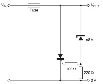
FIG. 11 Crowbar: excess voltage trip circuit can be used to protect
the load of a SMPS
If you need to isolate the SMPS for testing, you should connect a dummy load, and the ideal type of dummy load is an incandescent lamp with the appropriate power and current rating. Another safeguard is to obtain the input from a Variac™ autotransformer, allowing the a.c. input to be increased gradually. Yet another way of protecting the SMPS while under test is to include a 60 W lamp in series with the mains supply. The positive temperature coefficient of the lamp will guard against surges and protect against short-circuits.
The behavior of SMPS can be effectively studied using SMPS kits.
These not only provide valuable construction exercises and are useful as transistor-transistor logic (TTL)-type power supplies, but also can be used to study the regulation and ripple characteristics of SMPS. In the absence of a suitable training kit, an ideal substitute is a power supply unit from a computer. These are now inexpensive and readily obtainable items that can provide considerable experience with SMPS, although it is not always easy to obtain a circuit diagram.
You should record carefully voltages and waveforms for the SMPS working normally, and also in various fault conditions.
===
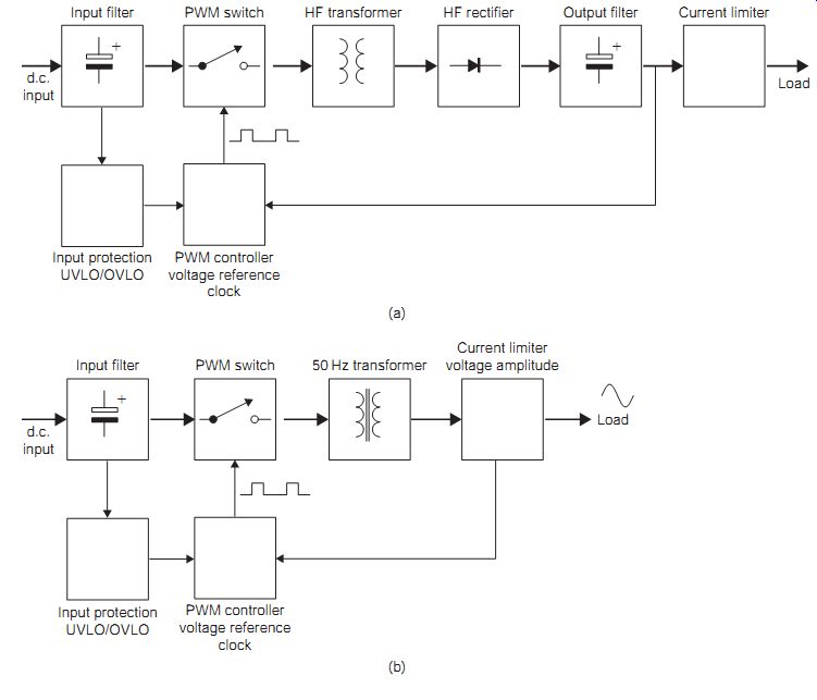
FIG. 12 Block diagram of: (a) d.c.-d.c. converter, and (b) an inverter
===
Inverters and converters
Although inverters are primarily designed to convert d.c. power into a.c. power, they have some features in common with converters, which are used to transform d.c. energy from a low-voltage level into d.c. at a higher voltage or d.c. of reverse polarity. The block diagram of FIG. 12 shows some of these common features. An oscillator, usually running at an ultrasonic frequency (typically around 20 kHz), is powered from a d.c. source. This oscillator drives a transformer either to provide an a.c. output in the case of an inverter, or to power a rectifier/smoothing circuit for converter applications. It is important to note that in each case the total output power must be lower than that supplied from the d.c. source owing to the energy losses in the transformer, etc. Using a rectifier bridge and smoothing or regulation in conjunction with an inverter produces a converter. Typical applications include producing d.c. at a higher or lower voltage or inverting polarity, so that a _5 V input can provide a -5 or -12 V output.
Many low-power, up to about 300 W, mains inverter designs are based on the use of an audio amplifier driving a mains transformer secondary with a 50 Hz sine wave so that the output from what would have been the mains primary is a 240 V r.m.s. sine wave at 50 Hz. Such systems typically use a full load drive current of 15-25 A r.m.s. from a 12 V source such as a car battery. Higher power inverters tend to be switch mode designs with a 50 Hz sine wave modulating the much higher frequency drive signal. This greatly reduces the power dissipation, as efficiencies approaching 85% can be achieved and much lighter and smaller ferrite transformers can be used.
FIG. 13 Typical line interference filters: (a) capacitor hf bypass,
(b) differential low-pass filter, and (c) common-mode low-pass filter
Interference reduction
When using mains-powered equipment it is important that the minimum of noise and interference generated should be fed back into the mains. This is particularly important where data-processing equipment is operating in close proximity to high-current industrial plant. Care is also needed where linear circuits are operating at low signal levels. Power supplies of the SMPS or oscillator types in particular should have their inputs well filtered to prevent pollution of the mains supply. For some linear circuits, the frequency of operation of the SMPS may have to be carefully chosen to avoid interference.
Interference can be continuous (as for SMPS) or transient (as when switching a supply on or off), and both radio frequency and transient suppression will be needed for most types of power supply.
Typical filter circuits and component values are shown in FIG. 13 (a-c). Inductors and capacitors used in these applications should have ad equate working voltage and/or current ratings under fault conditions. The characteristics of such filters are low pass, with zero attenuation at 50 Hz and at least 30 dB over the frequency range 150 kHz to 50 MHz. Data processing equipment is particularly susceptible to mains-borne interference. Data may be corrupted by the high voltage transients induced from inductive loads on the mains supplies. Fortunately, this problem is fairly easily solved by wiring devices called varistors across each pair of the mains supply wiring.
Varistors are particularly useful for transient suppression. These components are usually manufactured using zinc oxide or silicon carbide, with the former often being preferred because of its faster response. A varistor has a high resistance below some critical voltage, but above this, it rapidly con ducts to short-circuit any large overvoltage condition. The working voltages of these devices, which can be used for both a.c. and d.c., range from about 60 V up to about 650 V.
Mains power outlets and mains lead plugs are now available for low-power (less than about 2 kW) applications. These contain both filters and surge suppressors. They are particularly suited to the mains supplies for minicomputer and microcomputer installations.
Power supply units and other circuits that operate at high dissipation will usually contain safety-critical components. These are typically resistors with specified dissipation characteristics or capacitors that are constructed to avoid dangerous breakdown, and such critical components are usually marked as such on circuit diagrams.
The important point about such components is that they must be replaced, if found to be faulty, with the identical type of part, never with an ordinary component that seems to offer similar characteristics. Since a breakdown of such a component compromises safe use of the equipment, anyone replacing such a component with an ordinary one could be held responsible for the consequences of equipment breakdown.
QUIZ:
1. If a bridge rectifier is driven from an a.c. source, with peak voltage V' ac, what is the peak voltage across each diode?
(a) 2 V' ac
(b) 1.414 V' ac
(c) V' ac
(d) 0.5 V' ac.
2. A mains power supply uses a 24 V transformer and bridge rectifier, with a 10 000 µF smoothing capacitor.
If the output current is 1 A, what is the approximate output ripple voltage?
(a) 1 Vpp
(b) 0.7 Vpp
(c) 0.31 Vpp
(d) 0.1 Vpp.
3. In the previous question the mains frequency is 50 Hz. What is the ripple frequency?
(a) 25 Hz
(b) 50 Hz
(c) 100 Hz
(d) 200 Hz.
4. A shunt regulator circuit using a Zener diode is required to provide a load with a current of 5 mA at 6.8 V, when the input voltage can vary between 9 and 12 V (10 NiCd cells in series). What series resistor is required if the Zener requires a current of at least 5 mA for regulation?
(a) 470 O
(b) 220 O
(c) 180 O
(d) 160 O.
5. In question 4, what is the maximum power dissipated in the Zener diode?
(a) 34 mW
(b) 68 mW
(c) 126 mW
(d) 160 mW.
6. A series amplified Zener regulator supplies 5 V to a load at a current of 1 A, what is the dissipation in the pass transistor if the unregulated supply delivers 8.4 V at 1 A?
(a) 1 W
(b) 3.4 W
(c) 5 W
(d) 8.4 W