AMAZON multi-meters discounts AMAZON oscilloscope discounts
Revision
The bipolar junction transistor (BJT) and the field-effect transistor (FET) both control the current flow at their output terminals (collector and drain, respectively), and in both cases this current at the output can be controlled by the voltage at the input.
The ratio (Change in current at output/Change in voltage at input), with a constant supply voltage, is called the mutual conductance of the particular bipolar transistor or FET to which it applies. Its symbol is g_m. The values of mutual conductance obtainable from bipolar transistors are much greater than are those from FETs. In the mutual conductance graph shown in FIG. 1, for instance, a 30 mV input wave gives a 1 mA current flow at the output. The mutual conductance, gm, is therefore 1/0.03 _ 33.3 mA/V. Metal oxide semi conductor field-effect transistor (MOSFET) circuits are used for small-signal amplifiers mainly in integrated circuit (IC) form, although power MOSFETs are found in hi-fi amplifiers. The examples here are mainly for BJT circuits.
===
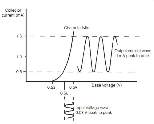
FIG. 1 Mutual conductance graph
with input and output waves indicated
===
The value of gm for a BJT depends mainly on the steady value of collector current, Ic, and is approximately 40 x Ic mA/V for any silicon transistor. If the collector load is Rc, then the gain is 40 x Ic x Rc.
Gain can be maximized by raising either the steady collector current or the collector load resistance, or both.
The method of operation for signal amplification is as follows. A signal voltage, alternating from one peak of voltage to the other, at the input produces a signal current, alternating from one peak of current to the other, at the output. To convert this signal current into a signal voltage again, a load is connected between the output terminal and the supply voltage. In a d.c. or an audio amplifier, a resistor can be used as the load, but for intermediate frequency (IF) or radio frequency (RF) amplifier circuits a tuned circuit (which behaves like a resistor at its tuned frequency) is used instead.
When the connection is in the common-emitter (CE) mode, the use of a load resistor causes the output voltage to be inverted compared to the input voltage. For example, a higher steady voltage at the input causes a greater current flow at the output. A larger voltage is therefore dropped across the load resistor, which causes the output steady voltage to be lower.
Any amplifying stage can give current gain, voltage gain and power gain, and the amounts of gain that can be obtained depend on the way in which the circuits are connected. FIG. 2 shows the three possible amplifying connections of a single transistor, with their relative gain values (bias components not shown).
===
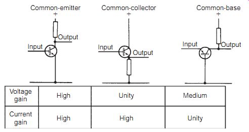
FIG. 2 Amplifying connections of a single transistor
==
Note that circuits using active devices such as bipolar transistors or FETs give power gain. The amount of this gain is calculated by multiplying voltage gain by current gain. Passive devices such as transformers can provide voltage gain or current gain, but not power gain. The additional power is supplied by the d.c. supply to the transistor.
The behavior of an amplifier can be clearly read from a graph of its output voltage or current plotted against its input voltage or current (for given values of load resistance and supply voltage). For example, the transfer characteristic of a small bipolar transistor is shown in FIG. 3. An input current wave of 50 µA peak-to-peak (p-p) produces an output current wave of 4 mA p-p. The current gain hfe of the transistor under these conditions is thus:
Collector current swing / Base current swing
= 4 mA/50uA =8
(Note that 4 mA _ 4000 µA.)
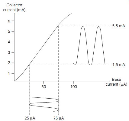
FIG. 3 Transfer characteristics of a small bipolar transistor
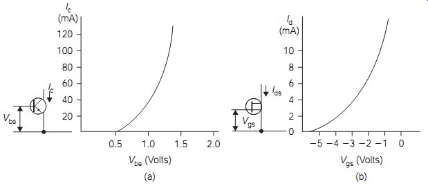
FIG. 4 Mutual characteristics of (a) a typical bipolar transistor,
and (b) a typical junction FET.
The current wave that is produced is in this case an exact copy of the input wave, because the part of the graph that represents the values of input and output current is a straight line. Because a straight-line characteristic produces a perfect copy, such an amplifier is called a linear amplifier. If the input signal had been greater, with peak values 0 and 100 µA, the output signal would not have been a perfect copy of the input wave because these values of input would make use of the part of the characteristic that is not a section of a straight line. A transistor working in linear conditions is also said to be working in class A (see later).
FIG. 4 shows the plots of the output current/input voltage characteristics of (a) a bipolar transistor and (b) a junction field-effect transistor (JFET). The curved shape of these characteristics shows that reasonably good linear amplification is possible only if a small part of the characteristic is selected for use. It is not, for example, possible to use an input voltage of less than 0.6 V for the bipolar transistor.
Another way of looking at transistor or FET action is by drawing the output characteristic. In the illustration of FIG. 5 each line is the graph of Ic plotted against Vc for a given base current Ib. The difference in spacing shows that amplification will be non-linear. In other words, if the output characteristic lines are drawn for equal changes in input voltage or current, the unequal spacing of the lines indicates that the transfer characteristic must be curved, producing non-linear effects. Such effects produce distortion, meaning that the shape of the signal wave will be altered.
===
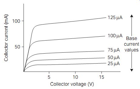
FIG. 5 Typical output characteristic
===
Bias
The mutual characteristics of the bipolar transistor shown in FIG. 4(a) made it clear that if such a transistor is to be used as a linear amplifier, the output current must never cut off, nor must the output voltage be allowed to reach zero (its bottomed condition).
Ideally, when no signal input is applied, output current should be exactly half-way between these two conditions. This can be achieved by biasing, by supplying a steady d.c. input which ensures a correct level of current flow at the output. A correctly biased amplifier will always deliver a larger undistorted signal than will an incorrectly biased one.
A correctly biased amplifier operating in such conditions, with the output current flowing for the whole of the input cycle, is said to be operating under class A conditions.
===
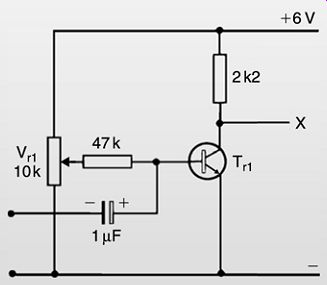
EXPERIMENT 1
Connect up the circuit shown in FIG. 6, in which Tr1 can be any medium-current silicon NPN transistor such as 2N3053, 2N1711, 2N2219 or BFY60. Set the signal generator to deliver a signal of ...
===
Bias circuits
Three types of bias circuit are illustrated in FIG. 7. The simplest uses a single resistor connected between the supply voltage and the base of the transistor (FIG. 7a). This type of bias is not used for linear amplifier stages because it is difficult to find a suitable value of bias resistor and the bias is greatly affected by changes in transistor characteristics caused, for example, by changes in temperature.
The circuit shown in FIG. 7(b) represents a considerable improvement, because the bias resistor is returned to the collector of the transistor rather than to the fixed voltage supply line. This small change makes the bias self-adjusting because of d.c. negative feedback, and the bias is now said to be stabilized.
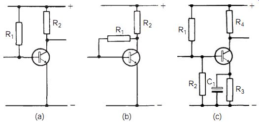
FIG. 7 Bias systems: (a) simple, (b) current feedback, and (c) fixed
base voltage type
The third bias circuit, shown in FIG. 7(c), is the most commonly used of all for discrete transistor amplifier circuits, either BJT or FET. The negative feedback system of biasing is the main (and usually the only)
method of biasing IC amplifiers (see later in this section). A pair of resistors is connected as a potential divider to set the voltage at the base terminal, and a resistor placed in series with the emitter controls the emitter current flow by d.c. negative feedback. Note that the emitter current is practically equal to the collector current flow (Ic= Ie + Ib, but Ib is very small).
In this type of circuit, the replacement of one transistor by another has little effect on the level of steady bias voltage at the collector, and changes caused by altering temperature similarly have very little effect. This biasing arrangement is therefore ideal for use in mass-produced circuits which must behave correctly even when fitted with transistors having a wide range of values of hfe.
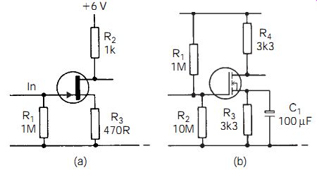
FIG. 8 Biasing circuit for: (a) junction FET, and (b) MOSFET
FIG. 8 illustrates the bias method (a) which is used for a FET in the depletion mode, and the circuit (b) commonly used for MOSFET biasing.
For correct bias, the voltage of the gate for the FET types illustrated here should be negative with respect to the source voltage or, to put it another way, the source voltage must be positive with respect to the gate voltage. In this circuit the positive voltage is obtained from the voltage drop across the resistor R3 in series with the source. The gate voltage of the JFET is kept at earth (ground level, or zero volts) by the resistor R1, which needs to have a very large value since no current flows in the gate circuit. The MOSFET circuit uses a potential divider (R1 and R2) to maintain a steady voltage on the gate, and the source is biased by the current flowing in R3. The calculations for the biasing of a FET are considerably simpler than for the biasing of a bipolar transistor.
Bias failure
Bias failure can be caused by either open-circuit or short-circuit bias components. In any of the circuits shown in FIG. 7, if a short-circuit develops across the resistor R1, the large bias current that will flow in consequence will cause the collector voltage to bottom, and may burn out the base-emitter junction. If the base-emitter junction thus becomes open-circuit, collector voltage will rise to supply voltage, so that the same fault can be the cause of either symptom. If R1 becomes open-circuit, there is no bias supply and the collector voltage cuts off, so that collector voltage equals supply voltage.
In the case of the circuit in FIG. 7(c), faults in resistors R2 and R3 can also affect the bias. Table 1 summarizes the possible faults and their effects.
===
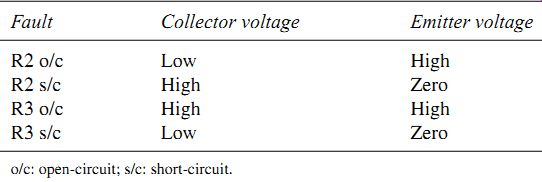
Table 1 Bias faults and their effects
===
Gain and bandwidth
The voltage gain (G) of an amplifier is defined as:
G = Signal voltage at output/Signal voltage at input
...with both signal voltages measured in the same way (either both r.m.s. or both p-p). This quantity G is an important measure of the efficiency of the amplifier and is often expressed in decibels by means of the equation: dB _ 20 log G.
Example: Find the gain of an amplifier in which a 30 mV p-p input signal produces a 2 V p-p output signal.
Solution: Insert the data in the equation G = (Signal voltage at output/Signal voltage at input), so that G = 2000/30 = 66.7. Note that the 2 V must be converted into 2000 mV, so that both input and output signals are quoted in the same units. Expressing the same answer in decibels, G =20 log 66.7 = 36.5 dB.
A decrease in gain from 66.7 to 60 might seem significant, but the same decrease expressed in decibels is only from 36.5 dB to 35.5 dB, a change of 1 dB, which is the smallest change of gain that can be detected by the ear when the amplifier is in use. Measurements of gain expressed in decibels can therefore show whether changes of gain are significant or not. Figures of voltage gain by themselves are often misleading for this purpose.
One very useful figure is the gain-bandwidth product, which is the result of multiplying gain by the frequency bandwidth (between the 3 dB points; see the following section). This is often quoted for transistors to allow estimation of the maximum possible bandwidth or the gain at different band widths. No amount of circuit tricks can increase the basic gain-bandwidth product of a transistor, a point that must be kept in mind when one transistor is substituted for another.
Frequency response
Voltage amplifiers do not have the same value of gain at all signal frequencies.
The circuit of FIG. 9 shows the components in a single-stage transistor amplifier that determine frequency response. (C4 is shown dotted because it consists of stray capacitances and is not an actual physical component.)
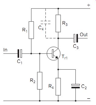
FIG. 9 Components that affect frequency response
In the circuit, C1 prevents d.c. from the signal source from affecting the bias at the base of the transistor, and C3 prevents d.c. from its collector from affecting the next stage. The circuit can therefore provide no voltage gain for d.c., and the amount of gain it can give at low a.c. frequencies is inevitably limited by the action of the capacitors C1 and C3. Gain for low frequencies will also be affected by C2, because this capacitor bypasses the negative feedback action of R4 for a.c. signals only.
At the high end of the frequency scale, the stray capacitances that are present at the collector of the transistor and in any circuit connected through C3 are represented by C4 connected across the load resistor. These strays act to bypass high-frequency signals, so that gain decreases at these frequencies also. Only in the medium range of signal frequencies most commonly used is the gain given by this circuit configuration constant. This constant value is often referred to as mid-range gain.
Note that raising the collector load resistance will provide more gain (if the steady bias current is not reduced), but will decrease the bandwidth.
A typical curve of gain (in decibels) plotted against frequency for such an amplifier is shown in FIG. 10. In this frequency-response graph, note that the frequency scale is logarithmic, so that 10-fold frequency steps occupy equal lengths of horizontal scale. This type of scale is necessary to show the full frequency range of an amplifier, and it normally plots gain in decibels.
==
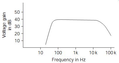
FIG. 10 Typical curve of gain plotted against frequency, for an untuned amplifier
===
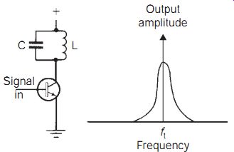
FIG. 11 Using a tuned circuit as a load and the typical output/ frequency graph shape
===
Note that these gain/frequency graphs apply only to sine-wave signals.
The response of any amplifier to sudden steps in voltage (transients) is affected by the slew rate of the amplifier, a topic that will be dealt with later, under the heading of Operational amplifiers.
When a tuned circuit is used as the output load of an amplifier (FIG. 11), the shape of the gain/frequency graph becomes more peaked. The reason is that the tuned circuit presents a high resistance to the signal at the frequency of resonance (fr). At resonance, this resistance has a value of L/CR ohms, where L is in henries, C in farads, and R is the resistance of the coil expressed in ohms. This value, L/CR, is called the dynamic resistance of the tuned circuit.
At all other frequencies, the load has a considerably lower value of resistance and acts instead like an impedance, with the result that voltage and current become out of phase with one another.
The gain of a tuned amplifier at the resonant (tuned) frequency is often controlled by an automatic gain control (AGC) voltage. This voltage is applied at the base (or gate of a MOSFET), either opposing or adding to the existing d.c. bias. Reverse AGC uses a d.c. bias voltage that reduces normal bias current, while forward AGC uses a bias voltage that increases the normal bias current. The type of AGC used depends on the type of transistor and the circuit of which it is a component.
To give forward AGC, a resistor is included in series with the load, but bypassed by a capacitor, so that signal current does not flow through it, and the transistor is so designed that its gain is much lower at low collector voltages. Increasing the bias current then lowers collector voltage and decreases the gain.
Most transistors, however, give greater gain at higher bias currents (given unchanged collector voltage), and so need to use reverse AGC.
==
EXPERIMENT 2
Use a single-stage transistor amplifier (designed so that the upper 3 dB point it not too high, for easy measurement), along with a signal generator, attenuator and oscilloscope to measure the lower and upper 3 dB frequencies. Measure the gain at the middle of the range (i.e. halfway between the lower and the upper 3 dB points) and calculate the gain-bandwidth. Make sure that the input is low enough to avoid noticeable signal distortion at the output. After making your measurements, increase the signal input until the output becomes distorted (not a sine wave). Sketch the output wave shape.
==
For an audio amplifier, the lower and upper 3 dB points (f1 and f2) are quoted, so that such an amplifier can be described as being, for example, 3 dB down at 17 Hz and at 35 kHz. For a tuned amplifier we usually quote the tuned frequency and bandwidth; for example, a bandwidth of 10 kHz centered on 470 kHz.
Table 2 lists faults that have predictable effects, especially on gain and bandwidth.
=====
Table 2: Amplifier faults
Fault | Effects
Emitter bypass capacitor o/c | Reduced gain, increased bandwidth
Collector load resistor too low | Low gain, increased bandwidth, d.c. voltage too high
Under-biased transistor | Gain reduced, signal distortion at output
====
Multiple-stage amplification
For most amplifier applications a single transistor is not enough to provide sufficient gain, and several stages of amplification are needed. When an amplifier contains several stages, its total gain, Gt , is given by the equation Gt = G1 x G2 x G3, where G1, G2 and G3 are the gains of the individual stages.
In decibels, this becomes: Total gain = dB1 + dB2 + dB3, giving the total gain in decibels. Note that the decibel figures of gain are added, whereas the voltage (or current, or power) figures have to be multiplied. This is because logarithms are used in the construction of the decibel figure, and addition of logarithms is equivalent to multiplication of ordinary figures.
The coupling together of separate amplifying stages involves transferring the output signal from one stage to the input of the next stage. This can be done in several ways, as described below and illustrated in FIG. 12 (from which details of all biasing arrangements have been omitted for the sake of clarity). The aim is to transfer the maximum amount of signal from one stage to the next.
===
Bias
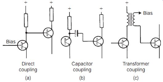
FIG. 12 Coupling amplifying stages: Bias Direct coupling Capacitor coupling
Transformer coupling (a) (b) (c)
===
Direct coupling involves connecting the output of one transistor to the input of the next, using only resistors or other components that will pass d.c.
The result is that both d.c. and a.c. signals will be coupled. A d.c.-coupled amplifier by definition amplifies d.c. signals, so that a small change in the steady base voltage of the first stage will cause a large change in the steady collector voltage of the next. In all d.c.-coupled stages, particular attention needs to be paid to bias. A negative feedback biasing system (see later) is usually required.
Capacitor coupling makes use of a capacitor placed in series between the output terminal of one stage and the input terminal of the next. The effect is that a.c. signals only can be coupled in this way, because d.c. levels cannot be transmitted through a capacitor. When amplifiers need a low -3 dB point when input frequency is only a few hertz, large values of capacitance will be required.
Transformer coupling makes use of current signals flowing in the primary winding of a transformer connected into the collector circuit of a transistor to induce voltage signals in the secondary winding, which in turn is connected to the base of the next transistor. Once again, only a.c. signals can be so coupled; and a well-designed transformer will be needed if signals of only a few hertz are to be coupled. Note that the gain/frequency graph of a transformer-coupled amplifier can show unexpected peaks or dips caused by resonances. For that reason, transformer-coupled amplifiers are seldom used when an even response is of importance.
Negative feedback
Negative feedback can be used in amplifier circuits either to stabilize bias ( d.c. feedback) or to stabilize gain (a.c. feedback), or both. The conventional bias circuit illustrated earlier is a form of d.c. negative feedback, and where stages are directly coupled (as in operational amplifiers; see later), d.c. feedback over several stages will be needed to stabilize bias. Fault-finding bias problems can be very difficult in such circuits because every component in the feedback path has an effect on bias. For the moment, however, we shall concentrate on the use of a.c. feedback.
Although it is possible to design single amplifier stages with fairly exact values of voltage gain (it is, for example, quite possible to design a single stage amplifier with a voltage gain of exactly 29 times, if that should hap pen to be wanted), it is less easy to design multistage amplifiers that will give the precise voltage gain required. The reason is that the input and output resistances of transistors vary considerably, depending on the varying hfe values of individual transistors, and that in any form of signal coupling the output resistance of one transistor forms a voltage divider with the input resistance of the next, so attenuating the signal.
The point is simply illustrated in FIG. 13, in which R1 symbolizes the output resistance of the first transistor and R2 the input resistance of the second.
===
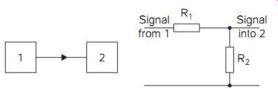
FIG. 13 Attenuation of a signal when coupled from one stage to another
===
A more useful way of designing an amplifier for a specified figure of gain is to aim for one which has much too large a value of voltage gain, and then to use negative feedback to reduce this gain to the required figure. Negative feedback means taking a fraction of the output signal and applying it to the input of the amplifier in antiphase. One advantage of using negative feed back is that it is often possible to calculate the gain of the complete amplifier without knowing any of the individual transistor gains or resistances.
Very often the gain of the amplifier is simply the ratio of two values of fixed resistors. Some feedback methods are shown in FIG. 14, illustrating how the feedback signal can be added to the input signal.
===
Feedback Input
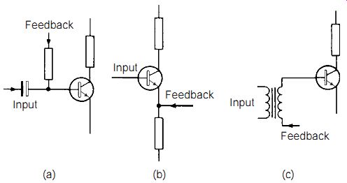
FIG. 14 Some feedback methods, omitting bias and supply components. (a) Shunt feedback to base, (b) series feedback to emitter, (c) series feedback using a transformer
===
For negative feedback to be useful, the gain of the amplifier without feedback (called the open-loop gain) must be much greater (100 times or more) than the gain of the amplifier when feedback is applied (the closed loop gain). When this situation exists, the feedback factor, (Closed-loop gain/Open-loop gain), becomes important, because distortion and noise generated in the transistors or other components within the amplifier will be reduced by exactly the same ratio. If, for example, closed-loop gain is 100 and open-loop gain is 10 000, then the feedback factor becomes 100/10 000, which is 1/100. This means that the distortion will be reduced to l/100th of its value in the open-loop amplifier.
Bandwidth, in contrast, will be increased by the inverse of the factor, which is 100 times in this example, on the assumption that there is nothing else that will limit bandwidth in any other way. You cannot, for example, expect negative feedback to make the bandwidth of an amplifier greater than the bandwidth that the transistor(s) will handle.
Note that negative feedback cannot improve the performance of an amplifier for pulse waveforms if the slew rate of the amplifier is being exceeded. This topic will be dealt with later as part of the limitations of operational amplifiers.
Experiment 3:
Test and diagnose a fault in a feedback amplifier.
Operational amplifiers
Operational amplifiers (commonly known as op-amps) were originally developed to perform the equivalent of mathematical operations in analog computers. Until integrated circuits were invented, however, their use in discrete form was very limited. Once mass production of integrated circuits started, op-amps were found to have many very useful properties for other applications. As a result, op-amps are now found in a very wide variety of equipment.
Integrated circuit op-amps are multistage differential amplifier units with direct coupling and very large values of gain. A differential amplifier is one that has two inputs, and it is the difference between the inputs that is amplified. The open-loop gain is the amount of gain that would be obtained by using the IC as an amplifier without feedback, but this amount is so large (usually 100 dB or more, corresponding to voltage gain of 100 000 or more) as to be unusable. Integrated circuit amplifiers are always used with negative feedback, and since direct coupling is normally used, the feedback is used both to establish bias and to establish signal gain. The advantages are:
• increased reliability due to a construction that leads to fewer interconnections to develop dry joints
• reduced size compared with their discrete-component counterparts
• reduced costs with volume production
• faster operation or better high-frequency response due to shorter signal path lengths
• IC fabrication gives a better control over the spread or variation of device parameters
• reduced assembly time due to fewer soldered joints.
Since the final performance of the circuit can be closely controlled by using negative feedback, the overall design of circuits is simpler.
A typical op-amp example, now quite old, is the 741. The remainder of this section will describe the operation of the IC version of this circuit.
The ideal op-amp would have the following characteristics:
• very high input resistance
• very low output resistance
• very high voltage gain, open-loop
• very wide bandwidth.
Table 3 shows typical characteristics for a 741 op-amp. You can see that the first three of the above requirements are easily met, while the bandwidth, although small by audio standards, is wide enough for the signals that the 741 was designed to handle, signals ranging from d.c. to a few hundred hertz.
===

Table 3
741 op-amp characteristics Input 1M Open-loop 100 dB Max. supply 18 V resistance gain voltage
Output 150R Bandwidth 1 kHz @ 60 dB Max. load 10 mA resistance gain current
===
The gain-frequency response of a typical op-amp is shown in FIG. 15.
Remember that by using negative feedback the stage gain of an amplifier is reduced, but at the same time its bandwidth is increased. This is due to the fact that the amplifier's gain bandwidth product is a constant. This feature of being able to trade gain for bandwidth is probably the most important feature of the op-amp and forms one of the design steps in the production of a practical amplifier, but care is needed because there are limits imposed by slew rate, as we shall see.
===
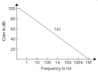
FIG. 15 Typical op-amp gain-frequency graph
===
The frequency range of an op-amp depends on two factors, the gain bandwidth product for small signals, and the slew rate for large signals.
The gain-bandwidth product is the quantity G x B, with G equal to voltage gain (not in dB) and B the bandwidth upper limit in hertz. For the 741, the GB factor is typically 1 MHz, so that, in theory, a bandwidth of 1 MHz can be obtained when the voltage gain is unity, a bandwidth of 100 kHz can be attained at a gain of 10, a bandwidth of 10 kHz at a gain of 100 times, and so on. This trade-off is usable only for small signals, and cannot necessarily be applied to all types of op-amp. Large amplitude signals are further limited by the slew rate of the circuits within the amplifier.
The slew rate of an amplifier is the value of change of output voltage per unit time: Slew rate = (Maximum voltage charge/Time taken), and the units are usually volts per microsecond. Because this rate cannot be exceeded for a given design of op-amp, the bandwidth of the op-amp for large signals, sometimes called the power bandwidth, is less than that for small signals.
The slew rate limitation cannot be corrected by the use of negative feedback; in fact, negative feedback acts to increase distortion when the slew rate limiting action starts, because the effect of the feedback is to increase the rate of change of voltage at the input of the amplifier whenever the rate is limited at the output. This accelerates the overloading of the amplifier, and can change what might be a temporary distortion into a longer lasting overload condition.
Slew rate limiting arises because of internal stray capacitances which must be charged and discharged by the current flowing in the transistors inside the IC, so that improvement is obtainable only by redesigning the internal circuitry. The 741 has a slew rate of about 0.5 V/µs, corresponding to a power bandwidth of about 6.6 kHz for 12 V peak sine-wave signals. The slew rate limitation makes op-amps unsuitable for applications that require fast-rising pulses, so a 741 should not be used as a signal source or feed (interface) with digital circuitry, particularly transistor-transistor logic (TTL) circuitry, unless a Schmitt trigger stage is also used. Higher slew rates are obtainable with more modern designs of op-amp; for example, the Fairchild LS201 achieves a slew rate of 10 V/µs.
The circuit symbol for an op-amp is illustrated in FIG. 16(a). Two power supplies are needed (although single supply lines can also be used by modifying the circuits). The dual supply is balanced about earth. The op-amp has two inputs, labeled (+) and (-), and a single output. The internal circuit is that of a balanced amplifier, so the output voltage is an amplified copy of the voltage difference between the two inputs. The (+) sign at one input indicates that feedback from the output to this input will be in phase, positive. The (-) sign at the other input indicates that feedback to this input will be out of phase, negative.
===
FIG. 16 (a) Op-amp symbol, and (b) basic phase-inverting amplifier circuit
===
FIG. 17 Op-amp circuits: (a) offset adjustment, (b) follower circuit, and (c) follower with gain
===
The voltage gain, open-loop, is some 10^5 (100 dB) or more. Since the internal circuit is completely d.c. coupled, both d.c. and a.c. negative feed back will be needed for linear amplifier applications.
An op-amp, unless the bias is stabilized, will suffer from drift and off set. Consider an op-amp with equal positive and negative power supplies.
If both inputs are at precisely the same zero-voltage level, you would expect the output also to be at zero (ground) level. In fact, it will not be, and the difference between input levels needed to obtain a zero output is called the offset. It might be possible to apply inputs that ensured a steady output (even if not zero), but in such conditions the output voltage would vary with temperature and time, the effect called drift. The problems of offset and drift are dealt with by using d.c. feedback bias circuits. See later for more details of drift and offset in practical circuits.
The diagram of FIG. 16(b) illustrates a basic phase-inverting amplifier circuit. Balanced power supplies are used, with the (+) input earthed and the (-) input connected to the output by a resistor Rf, which provides negative feedback of both d.c. and signal voltages. Rin serves to increase the input resistance. This inverting voltage amplifier circuit is the most common application for an op-amp.
Although the (-) input is not actually connected to earth, its voltage (either d.c. or signal) is earth voltage, and it is said for this reason to be a virtual earth. What happens is this. The (+) input is earthed, and any voltage difference between the inputs is amplified. Suppose, for example, that the (-) input is at 0.1 mV below earth voltage. This 0.1 mV will be amplified by 10^5 , giving a +10 V output (note the phase change). This voltage then drives current through Rf to increase the voltage at the (-) input until it equals the voltage at the (+) input.
Similarly, a 0.1 mV positive voltage at the (-) input would cause the output to swing to -10 V, again causing the input to return to zero. Two points should be noted:
• The voltage gain is so high that the assumption that the (-) input is at zero voltage is justified.
• Any unbalance in the internal circuit will cause an offset voltage at the input, so that the (-) input may need to be at a very small positive or negative voltage to maintain the output at zero (the input offset voltage).
This input offset can be reduced in the type 741 by adding the offset balancing resistor shown in the circuit of FIG. 17(a), in which the small figures are the IC pin numbers. The size of the offset voltage will, however, vary as the temperature of the IC varies, so that some compensation may be needed in circuits such as high-gain d.c. amplifiers, in which offset can be troublesome. This is known as the input offset voltage temperature drift, usually abbreviated to drift. The offset is not a problem when large amounts of d.c. negative feedback are used.
Owing to the virtual earth at the (-) input of the basic phase-inverting circuit, the circuit input resistance becomes equal to Rin. The figure for stage gain is simply the ratio Rf/Rin. To minimize the effects of temperature drift, the resistor R2 is made equal to the parallel combination of Rf and Rin; that is,
[...]
Again due to the virtual earth, several input signals can be applied to the (-) input through resistors. This forms the basis of the summing amplifier, where the input signals are added.
FIG. 17(b) shows a type of non-inverting circuit of the general type known as a follower. In this circuit the signal input is applied to the (+) input, whose d.c. value is normally fixed at earth voltage by R1. The feedback resistor R2 ensures that the (-) input is a virtual earth. A signal coming into the input will now produce an identical signal, in phase, at the output. The input resistance of the circuit is extremely high, the output resistance very low, and the circuit is used mainly to obtain these characteristics (like the emitter-follower transistor amplifier).
Unlike the familiar emitter-follower, this type of circuit can be modified to produce voltage gain, as shown in FIG. 17(c). Such a circuit should only be used when the signal input is of small amplitude, because the effect of the feedback is to make the input signal a common-mode signal, and the amplitude of common-mode signals needs to be kept below a specified value in most op-amp designs. The gain in the example is given by:
==
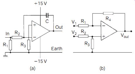
FIG. 18 Op-amp circuits: (a) integrator, and (b) differential amplifier
==
The characteristics of the op-amp make it possible to build integrating and differentiating circuits that give much better performance than can be obtained using only passive components.
FIG. 18(a) shows a simple op-amp integrator which functions also as a low-pass filter. The time constant CR2 seconds should be approximately five times the periodic time t of the input signal. A fully practical circuit, however, must also include some method of setting the output voltage to zero before the circuit is used, particularly if the d.c. level of the output is important. If the integrator is to be used for a.c. only, a bias resistor (such as R1) will serve to prevent drift.
If C and R2 of the integrator example are interchanged and their time constant is approximately one-fifth of the periodic time t, the circuit becomes a differentiator. The output waveform then depends on the rate of change of the input signal. For input signals of a different shape, the differentiator acts as a high-pass filter.
When an op-amp is operated in the differential mode as drawn in FIG. 18(b) (with bias omitted), its output, Vout , is proportional to the difference between the two inputs, V1 and V2. The polarity of Vout depends on which input is the larger. If V1 is the greater, then Vout is negative.
FIG. 19 shows positive feedback being used in an op-amp circuit.
This has the effect of providing a Schmitt trigger action with hysteresis. If we imagine the input voltage starting low, then with input voltage rising, the output will suddenly switch over (high). As the input voltage falls, the output voltage will switch back again, but not at the same voltage as caused the switch in the other direction.
FIG. 19 Op-amp providing Schmitt trigger action (power supplies omitted)
Op-amps can thus be used in many roles, the following being typical:
• as differential amplifiers, having exceptionally good common-mode rejection ratios, and with response down to d.c.
• as amplifiers for audio frequencies whose gain is controlled entirely by the values of the feedback components
• as high-pass and low-pass active filters
• as integrators and differentiators for the shaping of signal waveforms
• as sensitive switching circuits, triggered by the very small size of the differential input voltage needed to switch the output from one level to another
• as comparators, providing an output which is an amplified version of the voltage difference between two signal inputs (a.c. or d.c.). This application can be extended to provide a Schmitt trigger action with hysteresis.
[Test and diagnose a fault in an operational amplifier circuit.]
Power amplifiers
Both voltage amplifiers and current amplifiers play important parts in electronic circuits, but not all of them are capable of supplying some types of load. For instance, a voltage amplifier with a gain of 100 times may be well able to feed a 10 V signal into a 10 K load resistance, but quite incapable of feeding even a 1 V signal into a 10 ohm load. A current amplifier with a gain of 1000 may be excellent for amplifying a 1 µA signal into a 1 mA signal, but unable to convert a 1 mA signal at 10 V into a 1 A signal at the same voltage.
The missing factor common to both these examples is power. A signal of 1 A (r.m.s.) at 10 V (r.m.s.) represents a power output of 10 W, and the small transistors that are used for voltage or current amplification cannot handle such levels of power without overheating.
Transistors intended to pass large currents at voltage levels of more than a volt or so must have the following characteristics:
• low output resistance
• good ability to dissipate heat.
A low output resistance is necessary because a transistor with a high output resistance will dissipate too much power when large currents flow through it.
Low resistance is achieved by making the area of the junctions much larger than is normal for a small-signal transistor. The ability to dissipate heat is necessary so that the electrical energy that is converted into heat in the transistor can be easily removed. If it were not, the temperature of the transistor (at its collector-base junction) would keep rising until the junctions were permanently destroyed.
Given suitable transistors with large junction areas and good heat conductivity to the metal case, the problem of power amplification becomes one of using suitable circuits and of dissipating the heat from the transistor.
In practice, most power amplifier stages are required to provide mainly current gain, since the voltage gain can be obtained from low-current stages before the power amplifier stage. The power amplifier stage can therefore have very low voltage gain or even attenuate the voltage level.
Heat sinks
Heat sinks take the form of finned metal clips, blocks or sheets which act as convectors passing heat from the body of a transistor into the air. Good contact between the body of the transistor and the heat sink is essential, and silicone grease (also called heat-sink grease) greatly assists in this contact.
Many types of power transistor have their metal cases connected to the collector terminal. It is therefore necessary to insulate them from their heat sinks. This is done by using thin mica washers between the transistor and its heat sink, with insulating bushes inserted on the fixing bolts. Mica is an electrical insulator and a heat insulator, but for a thin washer the heat conductivity can be reasonably good. Heat-sink grease should always be smeared on both sides of all such washers.
Classes of bias
Several different methods exist for biasing transistors that are to be used in power output stages. Class A and class B are the names used for two types of commonly used biasing systems for audio, and class C is used for RF transmitter amplifiers.
The transistor in a class A stage is biased so that the collector voltage is never bottomed, nor is current flow ever cut off. Output current flows for the whole of the input cycle. It is the bias system that is used for linear voltage amplifiers. Class A operation of a transistor ensures good linearity, but suffers from two disadvantages:
• A large current flows through the transistor at all times, so that the transistor needs to dissipate a considerable amount of power.
• This loss of power in the transistor inevitably means that less power is available for dissipation in the load, and a class A stage can seldom be more than about 30% efficient, meaning that the a.c. power can seldom be more than 30% of the d.c. power.
Even in an ideal class A amplifier, with the load and amplifier output resistances matched, only some 50% of the available power would be delivered to the load, with the remaining 50% being dissipated by the amplifier in the form of heat. When the resistances are mismatched, the power transfer ratio is even lower.
In a class B amplifier (FIG. 20), the power transistor conducts for only one-half of the duration of the input sine wave. A single transistor is therefore unusable unless the other half of the wave can be obtained in some other way. At radio frequencies this can be done by making use of a load which is a resonant circuit (called a tank circuit). The tank circuit is made to oscillate by the conduction of the transistor, and the action of the resonant circuit continues the oscillation during the period when the transistor is cut off.
This principle can only be applied, however, if the signal to be amplified is of fairly high frequency. This is because the values of inductance and capacitance needed to produce resonance at, say, audio frequencies would be too large to be practical, and because a load of such a size would in any case restrict the bandwidth too much.
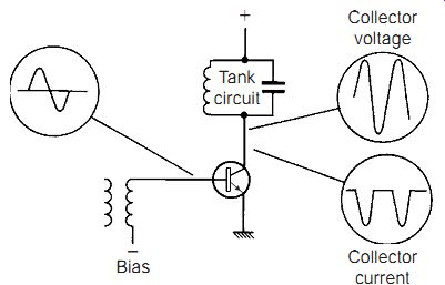
FIG. 20 Class B radio-frequency amplifier
An alternative method, which is used at audio and other low frequencies, is to use two transistors, each conducting on different halves of the input wave. Such an arrangement is called a push-pull circuit (FIG. 21). Push-pull circuits can be used in class A amplification, and are essential for use in class B audio amplifiers.
Input 1 Input 2 Signal output Bias
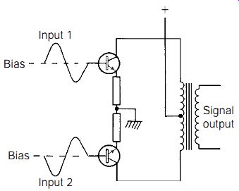
FIG. 21 Simple push-pull circuit using a transformer to combine the
antiphase outputs from the transistors Class B stages have the following
advantages over class A:
• Very little steady bias current flows in them, so that the amplifier has only a negligible amount of power to dissipate when no signal is applied.
• Their theoretical maximum efficiency is 78.4%, and practical amplifiers can achieve efficiencies of between 50 and 60%. This means that more power is dissipated in the load itself, and less wasted as heat by the transistors.
The disadvantages of Class B compared to Class A are that:
• The supply current changes as the signal amplitude changes, so that a regulated supply is often needed.
• More signal distortion is caused, especially at that part of the signal where one transistor cuts off and the other starts to conduct. This part of the signal is called the cross-over region.
The circuit of FIG. 22(a) illustrates a single-transistor power amplifier biased in class A. Because no d.c. can be allowed to flow in the load (which is in this case a loudspeaker), a transformer is used to couple the signal from the transistor to the load.
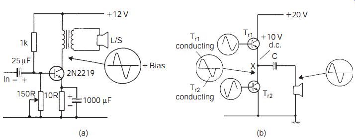
FIG. 22 (a) Simple class A stage, and (b) the single-ended push-pull
circuit
With no signal input, the steady current through the transistor is about 50 mA and the supply voltage is 12 V. Because of the low resistance of the primary winding of the transformer, the voltage at the collector of the transistor is about equal to the supply voltage.
When a signal is applied, the collector voltage swings below supply voltage on one peak of the signal and the same distance above the supply voltage on the other peak of the signal. Because of this transformer action the average voltage at the collector of the transistor remains at supply voltage when a signal is present.
In a class A stage of this type the current taken from the supply is constant whether a signal is present or not. Any variation in current flow from no-signal to full-signal conditions indicates that some non-linearity, and therefore distortion, must be present.
A circuit type that is often used for class B amplifiers is illustrated in FIG. 22(b). It is known as the single-ended push-pull or totem pole circuit. Two power transistors are connected in series, with their mid connection (point X in the figure) coupled through a capacitor to the load, which may typically be a loudspeaker, the field coils of a television receiver or the armature of a servomotor. During the positive half of the signal cycle Tr1 conducts, so that the output signal drives current through the load from X to ground. During the negative half of the cycle, Tr1 is cut off and Tr2 conducts, so that the current now flows in the opposite direction, through the load and Tr2.
The coupling capacitor C forms an essential part of the circuit. When there is no signal input, C is charged to about half supply voltage, i.e. the voltage at point X. The voltage swing at this point X, from full supply voltage in one direction to ground or zero voltage in the other, thus becomes at the load a voltage swing of the same amplitude centered around zero volts.
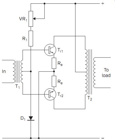
FIG. 23 Class A push-pull circuit
Bias and feedback
Class A output stages need a bias system that will keep the standing quiescent current (i.e. the d.c. current with no signal input) flowing through them almost constant, despite the large temperature changes caused by the standing current. One common method is to use a silicon diode as part of the bias network. The diode should be a junction diode attached to the same heat sink as the power transistor(s).
As a silicon junction is heated, the junction voltage (about 0.6 V at low temperatures) that is needed for correct bias becomes less. A fixed-voltage bias supply composed of resistors would therefore overbias the transistor as the temperature increased. A silicon diode compensates for the change in the base-emitter voltage of the transistor, since the forward voltage of the diode is also reduced as its temperature rises.
The class A push-pull stage in FIG. 23 uses two silicon transistors coupled to the load by a transformer. The input signal is also coupled to the stage by a transformer, which ensures that both transistors obtain the correct phase of signal. The use of a second transformer in such a circuit is often undesirable because it reduces the bandwidth and makes the amplifier less stable if negative feedback is used (because of the unpredictable changes of phase that occur in a transformer at extremes of frequency). A phase splitter stage that uses transistors rather than a transformer can be used. Such a phase-splitter can use a transistor with equal loads in collector and emitter, or a long-tailed pair circuit with unbalanced input and balanced output.
The bias current for this circuit is taken to the centre-tap of the secondary winding of the phase-splitter (or driver) transformer T1, and some additional stability is obtained by using the negative feedback resistors Re in the emitter leads. Any increase in the bias current of the power transistors will cause the emitter voltage of both transistors to rise, so reducing the voltage between base and emitter and thereby giving back-bias to the input.
In both the circuits that have been described so far the bias is adjusted so that the correct amount of steady bias current flows in the output stage. To adjust this bias current in the single-transistor stage requires breaking the collector circuit to connect in a current meter, and then adjusting a potentiometer so as to give the correct current reading. The push-pull circuit can be set by measuring the voltage across the emitter resistors, Re, and by adjusting VR1 to give the correct value of voltage at these points.
A more elaborate circuit using the class AB complementary stage is shown in FIG. 24. In class AB, each amplifier is biased to a value lying between those appropriate for either class A or class B. The output current in each stage thus flows for slightly more than half of each input cycle. The effect is to minimize the cross-over distortion that occurs in class B operation when both transistors are non-conducting.
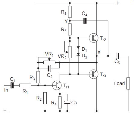
FIG. 24 Complementary class AB output stage of the totem-pole type
with driving stage and feedback connections
In this circuit, both a.c. and d.c. feedback loops are used. The d.c. feed back is used to keep the steady bias current at its correct low value, and the a.c. feedback is used to correct the distortions caused by class AB operation, in particular the cross-over distortion.
Two bias-adjusting settings are needed in this circuit. The potentiometer VR1 sets the value of the bias current in Tr1, so that the amount of current flowing through resistors R2, R3 and VR2 is controlled. The potentiometer is adjusted so that the voltage at point X is exactly half the supply voltage when there is no signal input. Potentiometer VR2 controls the amount of current passing through the output transistors.
This type of output circuit is called a complementary stage, because it uses complementary transistors, one NPN and one PNP type, both connected as emitter followers. With the emitters of both Tr2 and Tr3 connected to the voltage at point X, both output transistors are almost cut off when no signal is present. When VR2 is correctly adjusted, the voltage drop between points A and B is just enough to give the output transistors a small standing bias current (2-20 mA) to ensure that they never cut off together. The value of this steady current is usually set low, to keep cross-over distortion to a minimum. The actual value will be that recommended by the manufacturers. A current meter must be used to check the value of bias current.
Another name for this circuit is the Lin circuit, named after its inventor.
You can see that there are two a.c. feedback loops in this amplifier.
Negative feedback, to improve linearity, is taken through C2, and positive feedback is taken through C4 to point Y. This positive feedback, sometimes called bootstrapping, cannot cause oscillation in this circuit because the feedback signal is always of smaller amplitude than is the normal input signal at that point (an emitter follower has a voltage gain slightly lower than unity). It has, however, the desirable effect of decreasing the amount of signal amplitude that is needed at the input to Tr2.
Impedance matching
The ideal method of delivering power to a load would be to use transistors which had a very low resistance, so that most of the power (I^2 R) was dissipated in the load. Most audio amplifiers today make use of such transistors to drive 8 ohm loudspeaker loads.
For some purposes, however, transistors that have higher resistance must be used or loads that have very low resistance must be driven, and a trans former must be used to match the differing impedances. In public address systems, for example, where loudspeakers are placed at considerable distances from the amplifier, it is normal to use high-voltage signals (100 V) at low currents so as to avoid I^2 R losses in the lines. In such cases, the 8 ohm loudspeakers must be coupled to the lines through transformers.
To provide the maximum transfer of power, the turns ratio, N, of the transformer must be:
N = √ [Output impedance of amplifier/Impedance of load]
Faults in output stages
Faults in output stages are usually caused by overdissipation of power, which in turn can be caused by overloading or overheating. An output stage can be overloaded, when capacitor coupling is used, by connecting a load having too low a resistance. The usual result is to burn out the output transistor(s).
In most class AB totem-pole circuits, even the most momentary short circuit at the output (caused, for example, by faulty connections) will cause the transistor that is connected to the positive supply line (Tr2 in FIG. 24) to burn out if a signal is being amplified.
Excessive bias currents can often be traced to the failure of a diode in the bias chain, or to a burnout of the biasing potentiometer in a totem-pole circuit.
Unexpected clipping of the output can be caused by failure of the boot strap capacitor (C4 in FIG. 24), or by a fault in the bias resistors which has caused the voltage at point X to drift up or down.
Integrated circuit power amplifiers are now widely used, replacing power stages that use separate (discrete) transistors. Unlike op-amps, however, power amplifier ICs take no standardized form, although many use the same scheme of connections. FIG. 25 shows a circuit diagram (courtesy of RS Components Ltd) for the TDA2030 power amplifier used with a single 15 V power supply. The IC is manufactured on a steel tab which can be bolted to a heat sink for efficient cooling. Although this is now an old variety of IC, the principles are similar, and this age of component is likely to appear in equipment brought in for servicing.
===
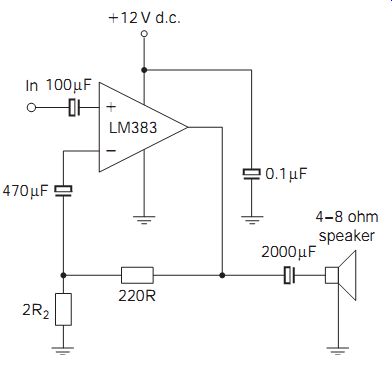
FIG. 25 An IC power amplifier circuit (National Semiconductor Inc.) using the LM383 IC
===
The circuit is very similar to that of a non-inverting op-amp voltage amplifier, but the practical layout of the circuit has to be designed so that the decoupling capacitors (C2 and C3) are very close to the IC. The electrolytic capacitor C3 needs to be bypassed by a plastic dielectric capacitor because the impedance of an electrolytic capacitor rises at the higher frequencies. At these frequencies, C2 performs the decoupling in place of C3. The series circuit of R6 and C6 is designed to maintain stability and is called a Zobel network; it is also widely used in discrete transistor amplifiers. This circuit will deliver up to 13 W of audio output into the 4 ohm loudspeaker.
Note that the circuits used in hi-fi amplifiers are usually of a specialized nature, and many use power MOSFETs in the output stages. Some types can be serviced, using information from the manufacturers, but others should be returned to the manufacturer for servicing, particularly if there has been a failure of any critical part. For example, failure of one power MOSFET will require replacement with a matching unit, and few servicing workshops will have equipment for precisely measuring power MOSFET parameters.
QUIZ
1. Increasing the value of the load resistance on a single-stage voltage amplifier will:
(a) increase the bias current
(b) decrease the bias current
(c) increase the gain
(d) increase the bandwidth.
2. Feedback of signal from the collector of a transistor directly to its base would cause:
(a) reduced gain
(b) more distortion
(c) oscillation
(d) reduced bandwidth.
3. A transformerless push-pull output stage might use:
(a) a stabilized power supply
(b) a phase splitter
(c) a Lin circuit
(d) high-resistance transistors.
4. A transistor amplifier is to be used at d.c. and very low frequencies. It cannot therefore use:
(a) negative feedback
(b) capacitor coupling
(c) a differential circuit
(d) balanced power supplies.
5. An ideal op-amp would have (among other things):
(a) very high output impedance
(b) very high input impedance
(c) very low gain
(d) very low common-mode rejection ratio.
6. At a virtual earth point you would expect to find:
(a) negligible d.c. voltage
(b) negligible feedback
(c) negligible offset voltage
(d) negligible a.c. voltage.