AMAZON multi-meters discounts AMAZON oscilloscope discounts
Positive feedback
Oscillators are critical to many systems: they act as clock sources for digital systems, carrier signal sources for radio transmitters, and sweep generators for television and oscilloscopes. Oscillators are usually built from amplifier stages and filter (delay) stages, using feedback to sustain the signal.
Negative feedback is achieved by subtracting a fraction of the output signal from the input signal of an amplifier. In practice, this is done by adding back the feedback signal in antiphase, so that feedback from an output which is in antiphase to an input is always negative unless some change of phase occurs in the circuit used to connect the output to the input (see later, under Oscillators for low frequencies).
If a signal which is in phase with the input is fed back, the feedback is positive. Positive feedback takes place when a fraction of the output signal is added to the signal at the input of an amplifier, so increasing the amplitude of the input signal. The result of positive feedback is higher gain (although at the cost of more noise and distortion) if the amount of feedback is small.
If the amount of feedback is large, the result is oscillation.
An amplifier will oscillate when both of the conditions below are met:
• The feedback is positive at some frequency.
• The voltage gain of the amplifier is greater than the attenuation of the feedback.
For example, if 1/50th of the output signal of an amplifier is fed back in phase, oscillation will take place if the gain (without feedback) of the amplifier is more than 50 times, and if the feedback is still in phase.
Oscillator feedback circuits are arranged so that only one frequency (called the fundamental) of oscillation is obtained. This can be done by ensuring that:
• the feedback is in phase at only one frequency
• the amplifier gain exceeds feedback loop attenuation at one frequency only, or
• the amplifier switches off entirely between timed conducting periods.
Oscillator circuits are of two types. Sine-wave oscillators use the first two methods above for ensuring constant frequency operation. Aperiodic (or untuned) oscillators, such as multivibrators, make use of the third method.
Oscillators are equivalent to amplifiers which provide their own inputs.
They also convert the d.c. energy from the power supply into a.c. Some oscillator circuits operate in class C conditions. Even if the transistors start off with some bias current flowing, the action of the oscillator will turn off the bias for quite a large proportion of the complete waveform, making the transistor operate in class C once it is oscillating. The reason for this will be clearer as you read through this section; it arises because a tuned circuit connected to an oscillator will continue to oscillate for a short time even when the transistor is no longer conducting. Aperiodic oscillators all operate in class C.
Sine-wave oscillators
A sine-wave oscillator consists of an amplifier, a positive feedback loop and a tuned circuit which ensures that oscillation occurs at a single definite frequency. In addition, there must be some method of stabilizing the amplitude of the oscillations so that the oscillation neither stops nor builds up to such an amplitude that the wave becomes distorted by reason of bottoming or cut-off.
The most common types of sine wave oscillator are those which operate at radio frequencies, such as are used in the local oscillators for superhet receivers, which use LC tuned circuits to determine the oscillating frequency.
Like most oscillator circuits, the Hartley oscillator exists in several forms, but the circuit illustrated in FIG. 1(a) is a much-used type. The tuned circuit L1C2 has its coil tapped to feed a fraction of the output signal back through C4 to the emitter of Q1. Since an output at the emitter is always in phase with the output at the collector, this feedback signal is positive. The base voltage of Tr1 is fixed by the values of the resistors R1 and R2, with C1 acting as an a.c. bypass capacitor.
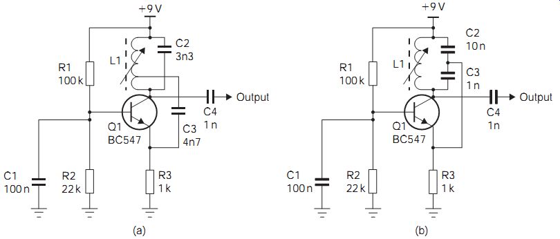
FIG. 1 Radio frequency LC oscillators: (a) Hartley, and (b) Colpitts
The amplitude of the oscillation is limited at the emitter because the transistor will cut off if the emitter voltage rises to a value more than about 0.5 V below base voltage. The distortion of the waveshape caused by this limiting effect is smoothed out by the flywheel effect of the tuned (or tank) circuit L1C2, which produces a sine-wave voltage at the resonant frequency even when the current waveform is not a perfect sine wave.
Irrespective of how its feedback is arranged, the Hartley oscillator can always be recognized by its use of a tapped coil. Its frequency of oscillation, as is the case with all oscillators using LC tuned circuits, is given by the formula:
f = 1/2pi √LC
Faults that can cause failure in an oscillator of this type include the following:
• bias failure caused by breakdown of R1, R2 or R3
• a faulty bypass capacitor
• a leaky or open-circuit coupling capacitor C4
• faults in either C2 or L1.
C2 should be a high Q, low loss part, typically polystyrene or multilayer ceramic using a high Q dielectric (C0G or NP0). In some older equipment silver-mica type capacitors were used, but these are now mostly obsolete and are not available in surface-mounted versions. Some low Q capacitors (X7R or Y5V dielectric) will not permit oscillation because of losses, meaning that the capacitor dissipates so much power that the loop gain falls below unity.
More often, lossy capacitors degrade the frequency stability of the oscillator.
The Colpitts oscillator (FIG. 1b) is basically similar to the Hartley oscillator. Instead of using a tapped coil, however, the Colpitts oscillator uses the combination of C2 and C3 to tap off a fraction of the output voltage to feed back into the base. The latter is biased and bypassed in the same way as in the Hartley circuit.
The same remarks about circuit operation, and about the several possible circuit configurations, apply to the Colpitts as to the Hartley oscillator, but the formula for determining the frequency of oscillation is slightly different.
Because the capacitors C2 and C3 are in series, it is the series combination C_ (in which l/C' = 1/C2 +1/C3) that tunes L1 to give the output frequency.
The formula must therefore use the value of C' rather than C2 or C3.
The oscilloscope is the most certain way of checking that an oscillator circuit is working, and also of measuring the frequency. Another check is to measure the current drawn by an oscillating circuit, which will be much larger than normal if the circuit is not oscillating (because the oscillator operates in class C when oscillating, requiring less bias current).
[[ Construct the Colpitts oscillator of FIG. 1(b). The inductor should be approximately 50 turns of 28 swg wire on a 10 mm ferrite core, or a 50-200 µH fixed inductor may be used. Use an oscilloscope to measure the signal at the collector of Q1. Measure the frequency of oscillation, adjust the power supply voltage to 12 V and measure the frequency of oscillation again. Warm the circuit gently with a hair dryer: what happens to the frequency of oscillation? ]]
Tuned-load oscillators (FIG. 2) have a tuned circuit as the load of the transistor and use another component for feedback. These oscillators are essentially variants of the Hartley oscillator described previously.
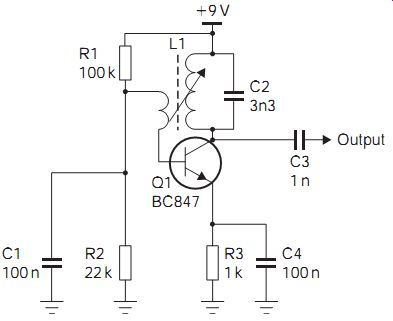
FIG. 2 Tuned load oscillator
Remember that the output of a single-transistor common-emitter amplifier is always phase inverted, so that another inversion must be carried out if feedback is to be taken from the collector to the base. One way of achieving this is to use a coupling winding on the same former or close to the collector inductor, connected to give a phase inversion. Amplitude limiting is carried out in this circuit by the bottoming and cut-off action, and the output is smoothed into a sine wave by the resonant oscillations of the tuned circuit.
Failure of this type of oscillator circuit can be caused by the bypass capacitor C4 going open-circuit, as well as by any of the biasing faults that can cause the Hartley oscillator to fail.
Crystal oscillators make use of a quartz crystal in place of a tuned circuit, to give much greater frequency stability than can be achieved under the same conditions by any LC circuit. Crystal resonators can easily achieve loaded Q values in excess of 10 000, compared with a good LC resonator with a loaded Q of 100.
There is a great variety of crystal oscillator circuits, some of which use the crystal as if it were a series LC circuit, with others using it as part of a parallel LC circuit in which the crystal replaces the inductor. FIG. 3 illustrates a form of Colpitts oscillator, but with the crystal providing the frequency-determining feedback path and some of the 180º phase shift between collector and base. The choke L1 acts as the collector load across which an output signal is developed and also contributes to the phase shift.
In normal use, crystal oscillators are extremely reliable, but excessive signal current flowing through the crystal can cause it to break down and fail. The usual comments concerning bias and decoupling components also apply here. Oscillators of the same type and performance can also make use of surface acoustic wave (SAW) filters to determine frequency.
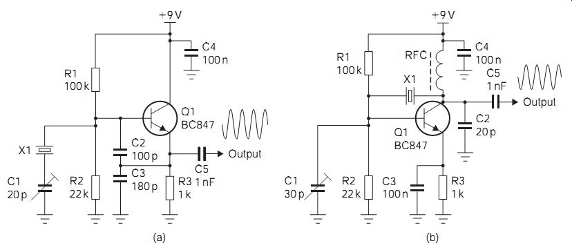
FIG. 3 Crystal oscillators: (a) Colpitts, and (b) Pierce
Note that all the circuits for sine-wave oscillators can be constructed with metal oxide semiconductor field-effect transistors (MOSFETs) in place of bipolar transistors. The use of MOSFETs has several advantages, particularly where crystal oscillators are concerned, because no input current is required at the gate of a MOSFET. However, MOSFETs are inherently noisier than bipolar transistors, so in high-performance oscillators their use may not be desirable; this is one of the few remaining applications where junction field-effect transistors (JFETs) can have an advantage.
FIG. 4 (a) Phase-shift oscillator, and (b) thermistor-stabilized Wien bridge circuit
Oscillators for low frequencies
Oscillators that are required to operate at low frequencies cannot use LC tuned circuits because of the impractically large size of inductor that would be needed. An alternative construction is the RC oscillator, and FIG. 4(a) shows the basic outline of one type, known as the phase-shift oscillator or divider-chain oscillator.
Every RC potential divider must attenuate and shift the phase of the signal at the collector of the transistor. If the total phase shift at a given frequency is 180º, the signal fed back to the base will be in phase with the signal at the collector and the circuit will oscillate.
The output waveform will not, however, be a sine wave unless the gain of the amplifier can be so controlled that it is only just enough to sustain the oscillation. All RC oscillators therefore require an amplitude-stabilizing circuit, which is usually provided by a negative feedback network. This net work usually includes a component such as a thermistor whose resistance decreases as the voltage across it increases.
In this way, an increase in signal amplitude causes an increase in the amount of negative feedback, which in turn causes the amplifier gain to decrease, so correcting the amplitude of oscillation. Failure in this feedback network will either stop oscillation or cause severe distortion of the output waveform.
Another type of RC oscillator is shown in FIG. 4(b). This type of oscillator is known as the Wien bridge. Note that the circuit uses feedback to the non-inverting (in-phase) input of the amplifier.
All RC oscillator circuits require amplitude stabilization if they are to pro duce sine waves of good quality, but they are capable of providing very low distortion figures (in the order of only 0.01%) by good design. The outline example of a Wien bridge oscillator circuit with provision for amplitude stabilization by a thermistor is illustrated in FIG. 5(b). The amplifier is a 741 integrated circuit (IC). A practical circuit would need to contain some setting to allow for adjustment of the feedback so that the thermistor could hold the amount of feedback at a level that would only just permit oscillation.
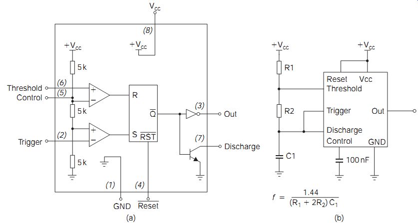
FIG. 5 (a) Simplified internal schematic for the 555 timer, and (b)
astable 555 circuit
A distorted output from an RC oscillator, or zero output, is nearly always caused by failure of a component in the amplitude-stabilizing circuit. Lack of output can also be due to a sudden loss of gain, such as could be caused by bias failure or by the failure of a decoupling capacitor.
[[ Construct the phase shift oscillator shown in FIG. 4(a). Use 220 k resistors for R1, R2 and R3, and 1 nF capacitors for C1, C2 and C3.
Adjust R5 so that the circuit just oscillates. Use an oscilloscope to monitor the output waveform at the collector of Q1. Sketch the wave form as R5 is adjusted. ]]
The 555 timer integrated circuit
The 555 timer is an IC that is widely used as an oscillator or as a generator of time delays. The timing depends on the addition of external components (a resistor and a capacitor), and one very considerable advantage of using the IC is that the time delays or waveforms that it produces are well stabilized against changes in the d.c. supply voltage. As with other ICs, we shall ignore the internal circuitry (other than a block diagram) and concentrate on what the chip does (FIG. 5).
The chip pin connections for the usual eight-pin dual in line (DIL) form of the chip are shown in FIG. 5(a), using pins 1 and 8 for earth and supply positive, respectively. The output is from pin 3, and the other pins are used to determine the action of the chip. Of these, pins 2, 6 and 7 are particularly important. Pin 7 provides a discharge current for a capacitor that is used for timing, and pin 6 is a switch input that will switch over the output of the circuit as its voltage level changes. For most uses of the chip, these pins are connected to a CR circuit, whose charge and discharge deter mine the time delay or the wave-time of the output.
An astable pulse generator circuit is illustrated in FIG. 5(b). Pin 6 is used to discharge the capacitor C1 and is connected to the triggering pin 2.
This ensures that the circuit will trigger over to discharge the capacitor when the voltage level reaches two-thirds of supply voltage, and will trigger back to allow the capacitor to charge when the voltage level reaches one-third of supply voltage. The frequency of the output can be adjusted by using a 100 K variable in place of R2 and, if needed, by using switched values of capacitance C1.
For the astable circuit illustrated, the waveform timings are given approximately by the following formulae:
Charge time: 0.7 (R1 + R2)C1 Discharge time: 0.7 R2C1 Periodic time: 0.7 (R1 _+ 2R2)C1 Frequency: 1.44/(R1+ 2R2)C1
[[ Construct an astable oscillator using a 555 timer IC. Using the circuit and formulae for frequency given in FIG. 5(b), select components that will give frequencies of 1 Hz, 1 kHz and 100 kHz, measure the output frequency of your circuit and comment on the component selection. Measure the supply current for each frequency. ]]
The voltage-controlled oscillator (VCO) is usually a standard LC oscillator circuit whose output frequency can be controlled by an input voltage applied at one terminal. One way of implementing this is to use an astable circuit in which the rate of charge and discharge is controlled by a transistor rather than a resistor. For higher frequencies, the VCO is usually implemented by using a varactor diode (FIG. 6) as part of the tuned circuit of an oscillator. Typically, a Colpitts circuit is used. The voltage control function allows the oscillator's output frequency to be controlled, either to make a frequency modulation (FM) modulator or by using a feedback control system to lock its frequency to a multiple of another frequency, using a phase-locked loop (PLL).
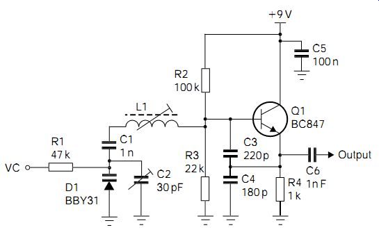
FIG. 6 Voltage-controlled oscillator
The PLL is an important circuit which forms the basis of many important functions in consumer, industrial and other electronic systems. PLLs are used in television receivers to synchronize the local colour decoder, as well as in synthesized tuners to select the channel frequency.
FIG. 7 shows the block diagram of the 4046, a common complementary metal-oxide semiconductor (CMOS) PLL IC. The heart of the circuit is an RC VCO circuit. The oscillator output is compared with that of an input signal, by one of several phase comparator circuits. If the difference between the VCO frequency and input signal frequency is within a certain range, the capture range of the loop, the loop locks and the oscillator frequency is pulled towards that of the input signal by the d.c. voltage generated by the phase detector.
===
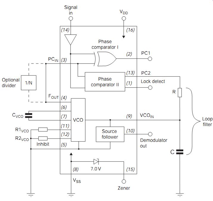
FIG. 7 Block diagram of the 4046 PLL IC
====
The 4046 can be used simply as a precision VCO whose frequency is set by the values of the resistors R1 and R2 and capacitor C1, as well as the voltage on pin 9 (FIG. 7). The output frequency is available at pin 4, the rest of the IC being disabled by connecting pins 3 and 14 to VSS and leaving pins 1, 2 and 13 unconnected. Alternatively, the PLL part of the 4046 can be used with an external VCO, the internal VCO being disabled by pulling the VCO inhibit pin, pin 5, high.
One common use of the 4046 is as an FM or frequency shift keying (FSK) detector. The internal oscillator frequency and tuning slope can be set over a wide range, and the bandwidth over which the internal oscillator will lock to the frequency of the incoming signal can be set by the choice of phase comparator and loop filter components. In this way the VCO can be made to track an incoming FSK or FM signal, with the original modulating signal being reproduced at the demodulate output pin, pin 10.
Using a divider circuit between pins 4 and 3 of the 4046 allows frequency multiplication by locking the VCO output divided by N to the input signal; for example, if the input to the PLL is a crystal-controlled square wave, the timing components can be set so that the output frequency is at N times the frequency of the crystal (provided that this does not exceed the frequency range of the VCO). The output frequency selected in this way will be perfectly locked in phase to the crystal frequency.
Such an arrangement is used in frequency-synthesizer circuits, since it can combine the versatility of the variable-frequency LC oscillator with the stability of crystal control. Component values for the loop filter, which determines how quickly the loop will lock and how the loop will follow a changing frequency input signal, can be calculated from the manufacturer's data sheet. These calculations are dependent on the phase detector being used and the exact details of the application.
A major advantage of PLL circuits is that they make it possible to regenerate a signal that is practically lost in noise. Provided the input signal amplitude is enough to drive the PLL (only about 180 mV is needed for the 4046 when operated from a 5 V supply), any input frequency that is within the capture range will be locked in, and the output will be a waveform of that frequency which is free from both noise and interference.
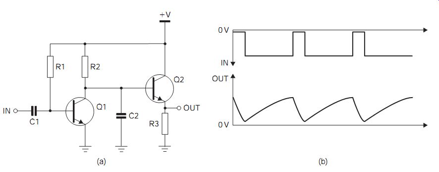
FIG. 8 (a) Simple timebase or sweep circuit, and (b) waveforms
Sawtooth generators
The action of an integrating circuit to convert a square wave into a wave with sloping sides makes it the basis for oscillator circuits that generate a sawtooth waveform used for time-bases. A simple timebase circuit is shown in FIG. 8. While Q1 is conducting, the voltage at its collector is very low and C2 is discharged. A negative-going pulse arriving (from an asymmetric astable multivibrator, for example) at the base of Q1 will cut off Q2, and C2 starts to charge through R2. This integrating action generates a slow-rising waveform which forms the sweep part of the sawtooth.
As the trailing edge of the pulse reaches its base, Q1 is switched on again.
C2 rapidly discharges through Q1 and causes the rapid flyback at the end of the sweep waveform. Q2 is an emitter-follower acting as a buffer stage to prevent the waveform across C2 from being affected by the input resistance of circuits to which the sawtooth is coupled.
In such a simple circuit, the waveform across the capacitor will, in practice, be approximately a straight line if C2 is allowed to charge only to a small fraction of the supply voltage. Thereafter, the waveform will tend to bend over towards the horizontal. To prevent this, it is important to make the time constant R2C2 much longer than the duration of the square pulse applied to the base of Q1.
Timebase circuits normally use considerably more elaborate methods than that shown in FIG. 8, with the object of ensuring that the sweep voltage remains linear. One type of sawtooth generator uses constant-current circuits to replace R2. Another, the Miller timebase, uses negative feedback to keep the sweep waveform more truly linear.
The Miller integrator is a circuit based on the application of negative feedback through a capacitor. In the circuit of FIG. 9, C1 (the Miller capacitor) is connected between the collector and the base of a transistor.
A rise of positive voltage at the input large enough to start the transistor con ducting would, if C1 were not there, cause a large negative change in voltage at the collector. Negative feedback through C1, however, prevents the voltage at the base of Q1 from rising more rapidly than the rate at which C1 can charge through R1.
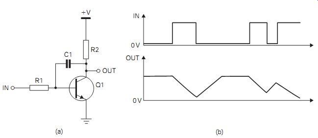
FIG. 9 (a) Basic Miller integrator circuit, and (b) idealized waveforms
This charging rate does not follow the usual exponential shape (while the transistor is conducting) because of the feedback through C1, and a good linear sweep waveform is obtained. The principal application of the Miller integrator is in timebase circuits for oscilloscopes. If the gain of the transistor is high, the sweep waveform can be made very linear indeed.
A complete Miller timebase circuit for an oscilloscope is made consider ably more elaborate than the basic circuit shown by the addition of other circuits whose purposes are (a) to discharge the Miller capacitor more rap idly (so obtaining rapid sweep flyback), and (b) to switch the input voltage at the times required to generate the timebase waveform.
QUIZ:
__1 What type of sine-wave oscillator uses a tapped inductor to provide the positive feedback required for oscillation?
(a) Clap
(b) Colpitts
(c) Hartley
(d) Pierce.
__2 What type of capacitor is usually used in the tuned circuits of oscillators?
(a) electrolytic
(b) low loss
(c) high voltage
(d) surface mount.
__3 An LC oscillator uses a 100 µH inductor.
What value of capacitor is required to tune it to 1.8 MHz?
(a) 16 pF
(b) 22 pF
(c) 47 pF
(d) 78 pF.
__4 An RC phase-shift oscillator uses three identical RC stages in the feedback circuit. What phase shift is required in each stage?
(a) 30º
(b) 60º
(c) 90º
(d) 120º.
__5 A timebase circuit uses a Miller integrator to produce the sweep signal for an oscilloscope. If the timebase circuit uses a bipolar junction transistor (BJT), where is the integrator capacitor connected?
(a) collector-emitter
(b) base-emitter
(c) collector-base
(d) base-positive supply