AMAZON multi-meters discounts AMAZON oscilloscope discounts
Part 4
Goals:
1. Demonstrate an understanding of logic families and their terms used in their specifications
2. Demonstrate an understanding of time division multiplex (TDM)
3. Demonstrate an understanding of sequential logic
4. Demonstrate an understanding of common fault types and an understanding of faultfinding procedures and test equipment.
Logic families and terminology
Digital logic devices may be members of families of standardized types, or they may be tailor-made for a particular application. At one time, digital circuitry was composed almost entirely of standard functions, that is gates, latches, dividers, etc., making replacement easy. Manufacturing cost and volume requirements tended to drive towards the use of the minimum parts count and hence application-specific integrated circuits (ASICs) that are made specifically to carry out all, or at least a large part of the required circuit functions. These ASICs are often hard to obtain as replacement parts, and are obsolete as soon as production of the products in which they are used ceases. Once the ASICs for a particular circuit are no longer available from the manufacturer, the repair of equipment that used the ASIC is no longer economically possible.
In recent years the emergence of very complex and powerful field programmable gate array (FPGA) chips has the begun to change the balance back in favor of repair and maintainability. This is because the FPGA chip can be reprogrammed relatively easily, and the parts are generally avail able from distributors. The use of reprogrammable technology has allowed manufacturers to reduce inventory because it is the software that defines the function of the FPGA and so a single FPGA may be used with different software in several products. Another advantage is that the manufacturer can make enhancements to the product in production without either waiting for new chips or scrapping the ones already in stock. Upgrades can even be performed in the field, often requiring just a laptop and an interface cable.
Despite the large-scale adoption of ASICs and FPGA, a large number of digital chips are still used that are manufactured in huge numbers and from many suppliers. It is important to be able to recognize and replace these devices. The four main features of a chip that is one of a standard family are:
• its type number
• the type of packaging
• the pin numbering and allocation
• the type of output.
Digital logic devices need to be provided with regulated supply voltages.
Almost universally now, a single positive regulated supply of +3.3 V or +5 V is used, with an earth (zero voltage) return, but a few chips may need both regulated positive and negative supplies and/or different voltages in addition to the earth connection. The supply current can range from a few nanoamps for some types of complementary metal-oxide semiconductor (CMOS) chip to several milliamps for the older transistor-transistor logic (TTL) types.
Microprocessors and complex programmable logic devices often use +3.3 V for their input-output interfaces and a lower voltage, such as 1.8 V, for the core logic. This is mostly to reduce the power consumption, and hence heat dissipation.
All digital devices specify an acceptable range for input and output signal voltage. Because of the development of logic chip types starting with TTL (see later), it has been customary to design other types of digital circuitry to use the same levels (TTL levels). These are:
• high level: +2.2 V to +5.5 V
• low level: 0 V to +0.8 V.
Threshold level is another important term that relates to the changeover from level 0 to 1 or from level 1 to 0. If we consider an integrated circuit (IC) that operates with TTL signals whose nominal voltage levels are 0 V and +5 V, the signals that are acceptable at an input need not be exactly at these levels; they will normally conform to the high and low range illustrated above. The values of +0.8 V and +2 V are the threshold levels, and any input between these levels is indeterminate; you cannot be sure what the output will be for an input that is in the threshold range. Digital circuitry must therefore be designed so that these intermediate levels exist only for a very short time during the change from 0 to 1 or 1 to 0.
The noise margin of a digital circuit is the amplitude of an unwanted input pulse that will just make the device switch over. This refers mainly to an input at the 0 level. For example, if the maximum possible input voltage level to guarantee logic level 0 is 0.8 V, and the specified maximum output representing a logic 0 is 0.4 V, then a positive-going noise pulse of greater than 0.4 V peak amplitude may be enough to cause the gate to switch over.
This value of 0.4 V is the noise margin (FIG. 1). It is more accurately described as the noise margin for logic 0, but since the noise margin for logic 1 is usually larger, this is the value that is normally quoted.
Noise margins are improved if digital circuits can be operated from higher voltages, so that the typical input levels of 0 V and +15 V that are used by the 4000 series of CMOS chips permit a much larger noise margin. The usual TTL type of circuit, however, is restricted to a +5 V supply, and noise problems are reduced by using a well-stabilized power supply with decoupling at each chip, and by using low-impedance inputs.
Modern microprocessor and allied chips often use metal oxide semi conductor (MOS) circuitry with a 1.45 V core supply used for processing actions, but using a 3.3 V level for (high) output. This reduces the dissipation within the microprocessor, but maintains a reasonably large noise margin at the output.
The input current of a device will be quoted at both signal levels. For TTL families, the input current at level 1 is very low, but the input current for logic 0 is substantial, several milliamps in the older designs. High-speed CMOS logic chips have input currents in the order of 1 µA, while some special-purpose low-power CMOS logic chips have very low input current figures in the order of 10 pA (10^-12 A) for either level of input. The output current range is usually between 1 and 5 mA for standard devices, but may be significantly more for high-speed gates or larger special-purpose output buffers.
===
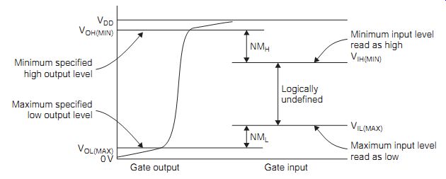
FIG. 1
Threshold levels and noise margin
===
Rise and fall times are the times needed to change input voltage levels from one threshold voltage level to the other, and are in the order of nanoseconds or picoseconds. A more important figure is propagation delay, which is the time between changing the input level and obtaining a corresponding change at the output. These times are in the order of 5 ns for most of the standard families of chips, but times measured in picoseconds (10^-12 s) are required for some purposes, notably fast ethernet (gigabit ethernet) and optical network components, as well as fast analog-to-digital (A-D) conversion.
Power dissipation for a chip can be high, several hundred milliwatts, for bipolar types, but for CMOS types it is low, typically several 100 µW, other than large-scale chips. For many digital circuits, the power dissipation of the standard logic chips is of little importance because so many circuits use fast microprocessor and memory chips dissipating tens of watts or more, so that the cooling requirements are fixed by the needs of these other chips.
Nevertheless, a packed logic board that uses only normal standard chip families may dissipate enough heat to require fan-assisted cooling.
The absolute maximum ratings for a logic chip define the levels that must not be exceeded, even for short periods. Any breakdown of regulation of a power supply will cause the absolute maximum voltage supply rating to be exceeded, so power supplies must contain some form of overvoltage cut off that will operate in the event of failure of regulation. Another common hazard is excessive input, because an input voltage may be obtained from some external circuit. Although MOS chips are protected by diodes to guard against damage from electrostatic voltages, these protection diodes are not capable of passing the more substantial currents that would pass in the event of a failure of power regulation in a unit that fed signal into a logic circuit.
Two terms that are very important to the operation of digital circuits are source and sink, applied to the current levels at an input or output of a digital IC. When we say that an output can source 15 mA, for example, we mean that the output can provide this maximum amount of current to whatever is connected to it. The connections will be either the inputs of other digital ICs, discrete circuits, or other loads such as micromotors.
The ability to sink current at an output means being able to allow inward current flow without an unacceptable change in voltage level. If we say that the input of an IC can accept a sink of 1 mA, for example, we mean that 1 mA can flow out of the input, and this current will flow to earth through the output terminal of the IC that drives this input, without causing the voltage at that point to rise unacceptably.
This leads to the term fan-out. The fan-out of a digital IC means the number of standard gate inputs that can be reliably driven from the out put. For example, if a gate output can sink or supply 16 mA, and its input requires sinking of 1.6 mA, then one output can be connected to as many as 10 inputs without compromising the ability of the circuit to operate.
Input connection is important for logic devices. No input must ever be left floating (disconnected) because this can lead to unexpected output changes, particularly at high clock rates when stray coupling can produce input voltages. The old TTL chips could be operated at slow clock rates, with an input left open-circuit, because the input to an emitter automatically ensured that the input level was at logic 1, but later types, and MOS chips in particular, must always have all inputs connected either to the output of another chip, or to one or other logic level through a resistor.
-------------
Experiment 1
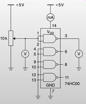
[... varying the input to the gate from 0 V to 5 V. Plot a graph of the
output voltage and supply current against the changing input voltage.
Repeat the experiment with a 74LS00 device, if one is available. Comment
on the difference in results. What would you check if replacing a faulty
7400 with 74HC00 device in a piece of equipment?]
----------
Device lettering and numbering
The two main logic families of devices are TTL and MOS, but there are several important subdivisions in each group. Originally, TTL meant a circuit in which each input was to the emitter of an IC transistor, with an output from a collector. A TTL circuit is designed to operate with a +5 V stabilized supply. Any voltage level above about 2.4 V at the input will be taken as being at logic level 1, and any voltage less than about 0.8 V at the input will be taken as being at logic level 0.
For example, FIG. 3 shows a circuit diagram that approximates to the internal circuitry of a TTL gate of the original 74 family, whose type numbers start at 7400 and continue into five- and six-figure numbers. The input stage consists of a transistor which has been formed with two (or more) emitters. This is comparatively simple to carry out when an IC is being formed, and 15 or more emitters can be formed on a single base of a transistor. The output stage makes use of the familiar totem-pole type of circuit, and the stages between these two will implement the gate action. They need not concern us here.
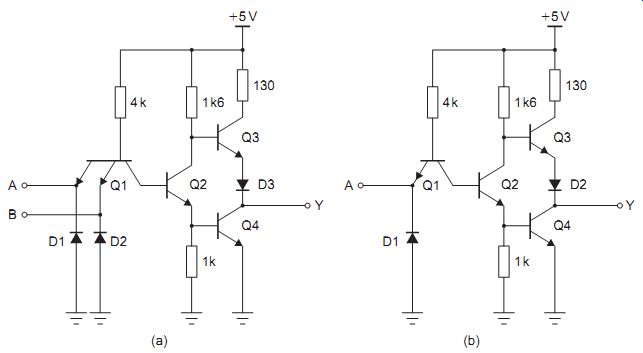
FIG. 3 Typical circuitry for: (a) standard TTL NAND gate, and (b) inverter
This type of IC family is now termed standard TTL, and is almost obsolete. The input impedance is low, so that an input current of about -1.6 mA must pass to an input to make the input transistor conduct. The output stage can sink or source a current of up to 16 mA, so that the maximum fan-out is 10.
Bearing these quantities in mind, we can now look at the operation of the typical standard TTL circuit in detail. The collector of the input transistor Q1 (FIG. 3a) is connected directly to the base of Q2. When both inputs, A and B, are connected to logic 1, always +5 V, no current will flow between the base and either emitter, since the base voltage is also +5 V connected via the 4 k resistor. The base-collector junction of Q1 forward biased current flows into the base of the following transistor Q2, which is thus turned on. In this condition, the top output transistor will be cut off, the base pulled low by the collector of Q2, and the output Y will be low because Q4 is conducting, turned on by Q2 emitter pulling its base up.
Now, if either one of the emitters is connected to logic 0, current will flow through the base of Q1 to the emitter which has been connected to logic 0. Because this current is large enough to saturate the transistor, the collector voltage will be low, and no current will flow into the base of Q2, which will now be cut off. In this condition current flows through the 1 k6 resistor into the base of Q3, causing this transistor to conduct and thus pulling the output Y up to the +5 V line, via D3. Q4 is cut off, its base tied to 0 V by the 1k resistor.
Since the output at Y is low only when both inputs are at logic 1, the action is that of a NAND gate, and the use of Q4 to connect the output 0 V ensures that comparatively large currents can pass from the terminal Y to the 0 V line without raising the voltage level of the output above the guar anteed low-level voltage. Remember that when a transistor is saturated, its collector-emitter voltage is low, typically 0.2 V, and does not rise appreciably when current flows. Ohm's law is not obeyed by a transistor junction because the internal resistance changes as current changes.
Standard TTL chips carry a guarantee that a current of up to 16 mA can be sunk at the output when Q4 is conducting. Because the current that Q3 can pass is limited by the value of the 130 ohm collector resistor within the IC, the maximum current that can be sourced when Q3 is conducting is limited to about 1 mA.
The input currents flow only from the emitters that are connected to logic level 0, and this is a maximum current of 1.6 mA per emitter. Since the maximum current (guaranteed) that can be sunk at an output is 16 mA, 10 times the maximum low-level input current for a guaranteed logic 0 level, this fixes the fan-out of a circuit of this type at 10.
All members of the 74 family of standard TTL chips use inputs that are transistor emitters, so that they pass current at logic level 0 and no current at logic level 1. The propagation delay, which is the time between changing the level at the input and finding a change at the output, is in the range of 11-22 ns (1 ns = 10^-9 s). The power dissipated per gate under average switching conditions is 10 mW, and the typical maximum operating frequency is around 35 MHz.
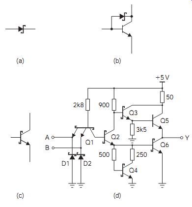
[FIG. 4 (a) Schottky diode symbol, (b) arrangement of Schottky diode and transistor, (c) Schottky transistor symbol, and (d) Schottky clamped TTL NAND gate]
At the time of writing, standard TTL chips are manufactured only for replacement purposes, although hundreds of millions of standard TTL chips are still in use. Another type of TTL circuit, the low-power Schottky transistor-transistor logic (LSTTL), largely replaced the standard variety because of the twin advantages of high speed of operation and lower power dissipation. The Schottky chips are identified by the use of LS in the type numbers, so that type 7400 is an standard TTL NAND gate, but 74LS00 is a low-power Schottky NAND gate. A faster version of Schottky clamped TTL is also available, designated 74S00, for example.
Low propagation delays that are obtained in standard TTL by using large currents inevitably lead to larger chip dissipation, because the current is flowing through the integrated components which are all part of the IC. The LS range of TTL ICs avoids this difficulty by using a different principle, relying on the use of Schottky diodes, components that can be made easily in IC form.
The Schottky diode, whose symbol is illustrated in FIG. 4(a), is formed by evaporating aluminum onto silicon, and its remarkable feature is its very low forward voltage when it is conducting, in the order of 0.3 V. This feature is used in two ways. One application is to carry out the logic action using the diodes in circuits similar to those used in the early diode transistor logic (DTL) ICs. The other use is in preventing the transistors in the circuit from saturating. A transistor is saturated when it is fully conducting, with the base passing more current than is needed to make the collector circuit con duct fully, since the collector current is limited by the value of collector load resistor. In this state, the collector-to-emitter voltage will be low, about 0.2 V, compared with the 0.6 V which will exist between the base and the collector.
When a transistor is saturated, there is a comparatively large amount of slow-moving charge in the base layer, and when the transistor is switched off by connecting the base terminal to the voltage level of the emitter, this stored charge will permit current to flow between the collector and the emitter for a time which can be as long as a microsecond, until the charge is neutralized. This restricts the speed at which a switching circuit can be operated, but if the transistors in switching circuits are not allowed to saturate, a very considerable increase in switching speed is possible. This can not, however, be achieved by normal biasing methods, particularly within an IC. Another advantage of using Schottky junctions is that they operate using majority carriers, so that the storage effect does not apply.
FIG. 4(d) shows the typical circuit of a NAND gate of the 74S family which uses Schottky transistors for logic, and also Schottky diodes for the input protection (D1 and D2) The Schottky connection within the transistor is between the base and the collector (FIG. 4b), so that when the transistor collector voltage approaches the saturation value, current from the base circuit is diverted by the Schottky diode into the collector circuit. This prevents the base current from reaching the value that would cause saturation. The Schottky symbol is shown on the transistor base (FIG. 4c) to make it clear that the Schottky diode structure exists within the transistor. The transistor circuit that is used within these Schottky TTL ICs is designed to make use of current stabilizers in addition to other methods of preventing saturation. Schottky clamped TTL gates designated 74S are much faster than their standard TTL counterparts, but this comes at the expense of increased power dissipation; for this reason, a low-power version was introduced, the 74LS series.
The 74LS series operates at the same voltage levels as the standard TTL 74 series, but the maximum output current is 8 mA and the input current at logic level 0 is +0.4 mA, one-quarter of the standard TTL current, so that the fan-out is 20. The propagation delay is in the range 9-15 ns, appreciably lower than that of standard TTL, and the average power per gate is about 2 mW. The typical switching frequency is 40 MHz.
Although most of the gates of the 74, 74S and 74LS series of TTL digital ICs make use of the totem-pole type of output circuit which has been illustrated, a few gates use open-collector outputs. This means that the phase-splitter and one-half of the output stage is missing, so that the out put terminal of such a gate is simply the collector terminal of a transistor.
If this gate is to be used in normal logic circuit applications, a load resistor, connected between the output and the +5 V supply line, must be added externally. Such outputs are used only in a few circuits where the outputs of several gates are connected, and the open-collector construction prevents a burnout when one transistor is at a high output and another connected to it is at a low output.
CMOS gate circuits
The most common semiconductor technology in current use is that of metal oxide semiconductor field-effect transistors (MOSFETs). Three types of IC can be manufactured using P- and N-channel field-effect transistors (FETs). PMOS ICs use P-channel FETs exclusively, NMOS ICs use N-channel FETs exclusively, and CMOS (C meaning complementary) ICs make use of both P- and N-channel FETs in a single circuit. PMOS methods were initially used for manufacturing microprocessors and similar chips, but were superseded by NMOS. Fast versions of CMOS are used in laptop computers.
One family of CMOS devices uses the 4xxx type of number, illustrated later, but the most common types currently in use follow the 74xx type of numbering, with lettering to distinguish the types, such as 74HC, 74HCT and 74AHC.
A typical CMOS NAND circuit, like that of one gate of the CD4011A or 74HC00 quad NAND IC is shown in FIG. 5(b). In this circuit, M1 and M2 are both P-channel types, whereas M3 and M4 are N-channel types.
The P-channel FETs will be switched into conduction by a logic 0 input at their gates, since their sources are connected to the positive supply.
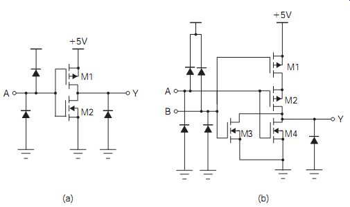
FIG. 5 (a) Typical CMOS inverter, and (b) NAND gate.
The N-channel FETs will be switched into conduction by a logic 1 input at their gates, because their sources are connected to the 0 voltage line.
With either or both gate inputs at logic 0, the P-channel FETs will con duct, keeping the output high. Only when both inputs are high can both N-channel FETs conduct, and thus connect the output to the logic 0 level.
The action is therefore that of a NAND gate. A NOR gate can be created using the same set of components by connecting the N-channel FETs in parallel and the P-channel FETs in series.
The 4000 series CMOS ICs can operate with a wide range of supply voltages, typically 3-15 V, and with very small currents flowing, 5 µA or less. The logic 0 and 1 voltages are normally very much closer to the supply voltage levels than is possible with older bipolar designs of the TTL, ECL or I2L types. For example, using a +5 V supply, a logic 1 voltage of +4.95 V and a logic 0 voltage of 0.05 V can be obtained. This makes for much better noise margins than can be achieved with either standard TTL or LSTTL devices.
The input current is always negligibly small because the inputs are connected to MOSFET gates, and the output currents of unbuffered gates are typically about 0.5 mA maximum. The fan-out figure for low-frequency operations can be very large, 100 or more, but the value decreases as the frequency of operation is increased. This is because the small currents that are available at the output must be capable of charging and discharging the capacitance at the input of each gate that is connected to the output. This requirement for charging and discharging stray capacitances also increases the total dissipation of the IC as the frequency of operation is increased.
A simple gate, for example, which has a dissipation of 1 µW at a frequency of switching of 1 kHz, may have a dissipation of 0.1 mW at an operating frequency of 1 MHz. This factor limits the operating speed of the earlier types of CMOS circuit, and leads to these types (the 4000 series) being used in low speed applications rather than for high-speed machine control or computing applications. They are widely used where speed is not of primary importance.
The very high insulation resistance of the gates makes them very susceptible to damage from electrostatic charges, and modern CMOS ICs are manufactured with a network of diodes connected to the inputs and outputs (FIG. 5), which will conduct whenever the voltage between gate and source or gate and drain becomes excessive. These diodes will typically protect a device for static voltages of up to 4 kV, but if higher voltages are likely to be encountered stringent earthing precautions must be taken. For example, operators may be required to use metal wrist straps that are earthed, and work on a conducting earthed surface. The safest way to work with CMOS devices is to earth all pins together until they are inserted into place and connected.
Note that walking along a nylon carpet can generate voltage levels in excess of 16 kV.
The original 4000 CMOS family of ICs typically used a 7 µm metal gate CMOS process which gave an absolute maximum supply voltage of about 18 V, although in operation the supply should be kept below about 15 V. Numbered from 4000 upwards, most of the standard functions were in the 40XX range, with some more complex ICs in the 45XX range. The numbers are suffixed with the letters B and UB; these suffixes indicate buffered and unbuffered devices, respectively. Buffered CMOS devices use a larger output stage to buffer the logic function, providing a higher current output. Since each stage is an inverter, a buffered device uses a chain of two inverter stages following the logic gate, and this adds to the propagation delay of the device.
The newer families of CMOS, based on a silicon gate process, used the numbering of TTL devices, with the letters HC, AC or LV, etc., so that a 74HC00 is a CMOS gate equivalent to the 7400 or 74LS00 in action, but with greatly reduced power consumption. These CMOS equivalents can be used, subject to some caution on their characteristics, as replacements for older bipolar standard TTL and LSTTL devices.
===
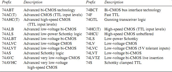
Table 1 Some 74 series logic families commonly available in 2006
Prefix Description Prefix Description 74ABT Advanced bi-CMOS technology 74BCT Bi-CMOS bus interface technology 74AC(T) Advanced CMOS (TTL input levels) 74F Fast TTL 74AHC(T) Advanced high-speed CMOS 74GTL Gunning transceiver logic
(TTL input levels) 74ALB Advanced low-voltage bi-CMOS 74HC(T) High-speed CMOS (TTL input levels) 74ALS Advanced low-power Schottky logic 74HCU High-speed CMOS unbuffered 74ALBT Advanced low-voltage bi-CMOS 74LS Low-power Schottky 74ALVC Advanced low-voltage CMOS 74LV Low-voltage CMOS 74ALVT Advanced low-voltage bi-CMOS 74LVC Low-voltage CMOS (5 V tolerant inputs) 74AS Advanced Schottky logic 74LVT Low-voltage bi-CMOS 74AVC Advanced very low-voltage CMOS 74LVTZ Low-voltage bi-CMOS live insertion 74AVHC Advanced very low-voltage 74S Schottky clamped TTL high-speed CMOS
===
The older 4000B series have typical propagation delays of 125-250 ns, power dissipation per gate of 0.6 µW and a typical switching frequency of 5 MHz. The unbuffered UB family features propagation delays of 90-180 ns and slightly higher typical frequency ratings. The 74HC family comprises direct replacements for 74LS types, with propagation times of 8-15 ns, power dissipation of 1 µW and typical frequency of 40 MHz. The 74HCT is very similar, but with slightly longer propagation delays; the T indicates that the input thresholds are set to match TTL levels rather than standard CMOS levels, i.e. they are fixed voltages rather than being a proportion of the supply voltage.
One of the more recent CMOS families is designated 74AC, with propagation delays of, typically, 5 ns, power dissipation of 1 µW and a typical frequency of 100 MHz. The 74LV family is optimized for very low supply voltages in the range 1.0-3.6 V; these devices are often used as 'translators' between low voltage microprocessors, e.g. 2.7 V, and standard 5 V logic systems.
The lettering used for more recent 74-series logic chip families can be con fusing, although the most common types have already been listed. Table 1 shows a more comprehensive list of known types in the year 2006. The quest for higher speed and lower dissipation continues, however, and several of the types in this list may become obsolete, with new types being introduced, during the lifetime of this guide.
===
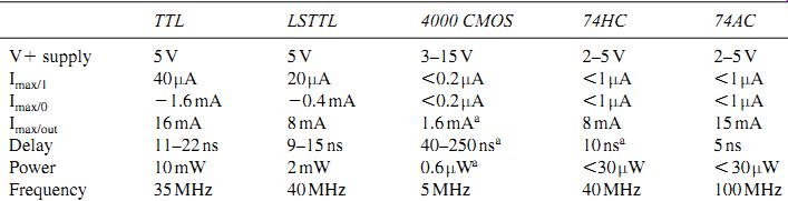
Table 2 Summary of logic family characteristics
Frequency 35 MHz 40 MHz 5 MHz 40 MHz 100 MHz V_ supply: normal positive supply voltage level; Imax/1: maximum input current for logic level 1; Imax/0: maximum input current for logic level 0; Imax/out: maximum output current; Delay: propagation delay in nanoseconds (a low delay means a fast device); Power: no-signal power dissipation per gate in mW or µW; Frequency: typical operating frequency.
===
Table 2 shows a comparison of the most common families of devices that use either the 7400 or the 4000 type numbers.
Some circuits, notably computer boards, feature chips that are described as having tri-state outputs. This does not mean that they use three logic states, only that the chip can be isolated from inputs and output by not applying an enabling pulse. The purpose of this is to allow a set of chips to be permanently connected to the same set of input and output lines, selecting which chips are in use by their enabling inputs. Tri-state logic chips are therefore extensively used in any circuits that make use of bus lines to connect different portions of the circuitry.
The packaging of the standard families of logic gate circuits is usually either plastic dual in line (DIL), for pin through hole parts, or small outline (SO) surface mount package. Leadless ceramic chip carrier (LCC) pack ages are available for high-reliability applications.
Gates are usually packaged in groups of four or six in a 14- or 16-pin package. Single gate chips are also available in surface-mount packages, either SOT23 or SC70; for example, the 74HC1GU04 is a single inverter in a SOT23 package. Such devices are commonly used in mobile devices to modify or buffer the output from an ASIC, etc.
The standard 14- and 16-pin logic ICs have two pins reserved for earth (pin 7 or 8) and V+ (pin 14 or 16). The conventional way to show pin allocations is a diagram that shows the top view of the chip with logic gate symbols and connections drawn in as illustrated in FIG. 6.
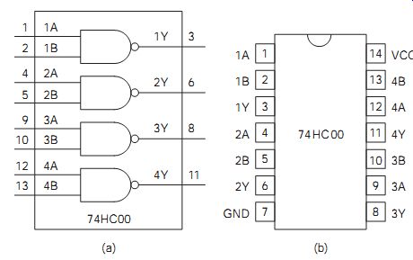
FIG. 6 Typical pin-out diagram for a logic chip.
QUIZ:
__1 How is the noise margin of a logic family defined?
(a) VOH - VOL
(b) greater of VDD - VOH and VOL - GND
(c) smaller of VIL - VOL and VOH - VIH
(d) VIH - VIL.
__2 A logic family has an input current of 1.6 mA and an output current of 8 mA. What is the fan-out of the family?
(a) 8
(b) 5
(c) 20
(d) 10.
__3 What parameter causes the main limit on fan-out of CMOS logic in high-speed applications?
(a) d.c. input current
(b) output current
(c) input capacitance
(d) power supply voltage.
__4 How are CMOS circuit inputs protected from electrostatic discharge damage?
(a) bipolar input stages
(b) low power supply voltage
(c) using both NMOS and PMOS transistors
(d) input protection diodes.
__5 Which common logic family can be used over a 3-15 V supply range?
(a) 74LS TTL
(b) 4000 CMOS
(c) 74HC CMOS
(d) standard TTL