AMAZON multi-meters discounts AMAZON oscilloscope discounts
Sequential logic circuits are those whose outputs depend not only on the current inputs, but also on the order that the inputs change. This means that the output depends on past as well as present inputs, so these circuits have 'memory' and are a very important building block for many complex systems, such as counters, timers and computers.
A flip-flop is a circuit of the bistable type. Integrated circuit (IC) flip-flops tend to be of complex designs that would be uneconomical to manufacture with discrete components. The simplest flip-flop is the R-S type.
The simple R-S flip-flop changes state when either of the inputs becomes, or is set to, zero. Most digital circuits require flip-flops that change state only when forced to do so by means of a pulse, called a clock pulse, arriving at a separate input. In a set of such clocked flip-flops, all the flip-flops in a circuit can be made to change state at the same time.
Clocking has the advantage that so long as the inputs can be guaranteed stable by the time the clock pulse arrives, the order that the inputs change in, or changes of state at the inputs at any other time, have no effect on the output. Between clock pulses, the output remains as it was when set by the last clock pulse.
The edge-triggered D-type flip-flop has inputs of data (D), clock (CLK), preset () PRE and clear () PRE ; with outputs of Q (main output) and Q# or Q, the inverse of the Q output. This flip-flop is triggered on the leading edge of the clock pulse. The logic value on the D (data) input is then transferred to the Q output, thus delaying the data by the period of one clock pulse. The truth table is illustrated in Table 1.
===
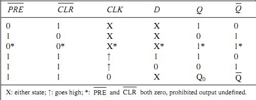
Table 1 D-type flip-flop truth table
===
Reference to the truth table shows the action of the preset and clear inputs to set the initial output states of the device. When () PRE = 0, Q is set to 1 and when CLR = 0, Q is set to 0. The states of both CLK and D are irrelevant (X) at this moment in time because () PRE and CLR override them. Only when PRE CLR __1 will the clock pulse transfer the data, and even then only as the clock pulse reaches a high value.
The state where PRE CLR __ 0 represents an unstable condition in a D-type flip-flop, and is prohibited.
The D-type latch (FIG. 1), sometimes called a transparent latch, is very similar to a D-type flip-flop, except it is level rather than edge triggered; that is, the outputs follow the inputs while the CLK pin is high and are held or latched at the last state once the clock pin goes low. When latched, the output value at the Q terminal remains at its previous setting, regardless of the input at D, until a clock pulse is applied. A latch is a very valuable component of digital circuits because it performs a form of memory action. The output ports of microcontrollers, for example, use a latch to hold the output data until it needs to be changed by the program.
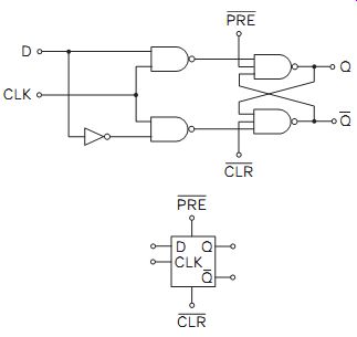
FIG. 1 Schematic and symbol for D-type latch
The J-K flip-flop, which also contains steering logic to avoid the output problem of the R-S flip-flop at R = 0, S= 0, also has a greater range of output controls, as shown by Table 2. This type of flip-flop has three signal inputs labeled S (set) and R (reset) (or sometimes preset and clear) which work independently of the clock pulses, and the usual two outputs Q and Q# (with Q# always the inverse of Q for any combination of inputs). The J and K inputs are programming inputs that determine what will hap pen when a clock pulse is applied.
If the complementary outputs of the J-K device change state before the end of a clock pulse, then because of the internal feedback, the inputs will also change. This can cause the device to oscillate until the end of the pulse and leave the output in an indeterminate state.
===
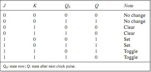
Table 2 State table for a J-K flip-flop J K Q0 Q Note
===
To avoid this race condition, the clock pulse duration should be small compared with the propagation delay. For high-speed operation, this is avoided by using a master-slave device as shown in FIG. 2, where the NAND logic gates act as switches. The state table is the same as for the simple J-K device.
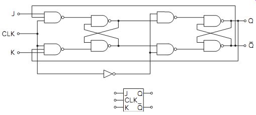
FIG. 2 Master-slave J-K flip-flop and symbol
Data is transferred in two stages on both edges of the clock pulse. On the positive edge, the input gates are enabled and allow the data to be loaded into the master flip-flop. At this time the output logic gates are open-circuit.
On the negative pulse edge, the switch states reverse, the master is isolated from the input and the data is transferred to the slave stage to provide the output. The master-slave design is preferred in most applications.
The binary counting action occurs when both J and K inputs are taken to logic 1 [ +5 V in the case of transistor-transistor logic (TTL) circuits]. Two clock pulses arriving at the clock terminal give rise to one pulse at the Q out put, while a pulse of inverse polarity will simultaneously reach the Q# output.
• Clock pulse inputs to digital circuits must have short rise and fall times, and the inputs to gates should never be slow-changing waveforms. The reason for this is that the gain of these circuits, considered as amplifiers, is very large, so that a slow-changing waveform at the inputs can momentarily bias the circuit in a linear mode, allowing it to amplify noise signals present in the circuit, which appear as a burst of pulses or oscillations. Oscillation can cause multiple counts and erratic operation.
• Logic circuits designed to tolerate slowly changing inputs use a Schmitt trigger input stage which uses hysteresis to reinforce the switching action and reduce the possibility of oscillation.
[[ Experiment 1
Connect the circuit shown in FIG. 3 using a 74HC74 IC on a breadboard. The 74HC74 contains two D-type flip-flops. Apply clock pulses either from a slow pulse generator or from a debounced switch (see Section 15), and observe the output indicator light-emitting diodes (LEDs). Now connect the clock terminal (pin 11 of the second flip-flop in the package) to the Q output (pin 5 of the first flip-flop), and reapply the slow clock pulses. Observe the indicators. Remember that no input pin may ever be left unconnected.
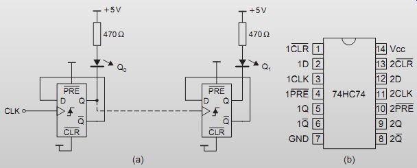
FIG. 3 Circuit for practical: (a) connections, and (b) pinout of
74HC74 IC ]]
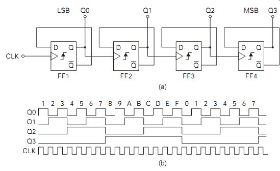
FIG. 4 Ripple or asynchronous counter: (a) circuit, and (b) counter
waveforms
A fundamental feature of all clocked bistable devices is that they can be used to divide the input number of clock pulses by two. Thus, for every two clock-pulse inputs, the Q output changes once. This concept forms the basis of electronic binary counters, an example of which is shown in FIG. 4.
The pulse sequence to be counted is the input to FF1, whose Q output now provides the clock for the next stage, and so on. This is an asynchronous counter. A count input to the first stage thus ripples through the circuit from one flip-flop to the next, which is why a counter of this type is often called a ripple or a ripple-through counter. Note that the output count should be read from right to left, because the most significant bit (MSB) is, by convention, shown on the right of the drawing. A chain of n flip-flops will, connected in this way, produce a counter that divides the number of input pulses by a maximum of 2n.
The ripple counter waveforms are shown in FIG. 4(b). Since the Q output is fed back to the D input, the Q output toggles, or changes, on the rising edge of every clock cycle.
FIG. 4 Ripple or asynchronous counter: (a) circuit, and (b) counter
waveforms.
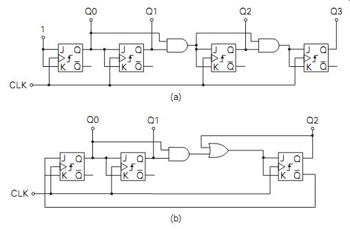
FIG. 5 (a) Synchronous 4-bit binary counter, and (b) synchronous
divide by 5 counter.
Ripple counters are unsuitable for applications such as timers where their output value needs to be decoded, because the delays incurred by the ripple progressing through the counter mean that the parallel decode output can have false-positive states. Although these are often only very short lived, of the order of tens of nanoseconds, the result can be to trigger erroneously the decoding logic. For this reason synchronous counters are always used where decoding of the count is required. Ripple counters are useful for frequency division, as in clock scaling and similar applications.
If the design of the counter is changed so that all the flip-flops are clocked at the same time (synchronously), the propagation delay is reduced to that of a single flip-flop, thus eliminating the race hazard and making it possible to decode the count successfully. For TTL counters, the maximum count frequency is about 50 MHz, compared with about 25 MHz for a 4000 CMOS counter. 74HC high-speed CMOS counters can operate at much higher speeds.
Synchronous counters can be constructed using J-K flip-flops and gates, and a typical circuit for a synchronous 4-bit counter is shown in FIG. 5(a). The J-K flip-flop changes state (toggles) only when J= K= 1 at the time of a clock pulse. The toggle action in this circuit is controlled via the Q outputs and the AND gates. Before any bistable can toggle, all the earlier bistable Qs must be at logic 1. Because J and K inputs of the least significant bit (LSB) flip-flop are connected to logic 1 it toggles on every clock pulse.
The second only toggles while the Q output of the first is high, the third while both the first and second flip-flops have high Q outputs, and so on.
You may need to divide by a number N which is not a power of 2; for example, to divide by 5 for part of a denary counter (FIG. 5b). A counter that carries out a division by N is called a modulo-N counter. There are several methods of designing such a counter. The state machine method defines the valid counts or states and then logic is designed to achieve the correct progression from each state to the next. FIG. 5(b) shows a divide by 5 circuit that is made in this way. Another design method that can be used for such counters is that of an interrupted count, meaning that the counter contains sufficient flip-flips for a longer count, but is interrupted after the count of N and reset to zero. This requires decoding logic for the value of N. Another method is the dual modulus counter. This is a counter that divides by N for part of the time and by M for the rest of the time. This allows average fractional counts and is often used in PLL frequency synthesizers.
To construct an interrupted count counter n flip-flops are needed, such that n is the smallest number for which 2n > N. A decoder circuit detects when a count of N has been reached so that the circuit can be reset to zero.
For a decimal counter n = 4, because 2^4= 16, which is the nearest number greater than 10. Denary 10 is 1010 in binary, so the feedback must detect this pattern to reset the counter to zero.
Integrated circuit counters
A count from zero to nine, followed by resetting, however it is achieved, is the basis of BCD counters, in which each counter unit (a set of four flip-flops) is used for one column of a denary number. BCD counting allows for the display of a count number to be simply decoded in denary rather than in binary, so BCD counters are preferred for any application in which a count is to be displayed rather than simply used.
BCD counters are available in IC form in the 74 series, and the simplest unit is the 7490. This is one of the very few IC counters that is classed as asynchronous, and is designed mainly for use with displays. The design is a split counter with one scale of two (a single flip-flop) and one scale of five which uses three flip-flops connected as a synchronous counter. For decade counting, the output of one unit is connected to the clock input of the other, so that the overall action is asynchronous. Because of the asynchronous action, the Q outputs will not change simultaneously, and this can give rise to spikes on the outputs. These are unimportant if the output is used to operate a display, since the display does not store the spike output, but it makes a counter of this type unsuitable if the outputs are connected to latches.
The pinout for the 7490 is shown in FIG. 6(a). The pins labeled MR1 and MR2 are reset inputs; which must both be taken to logic 1 to reset the counter, since they are inputs to a NAND gate. The inputs MS1 and MS2 are similarly used to set the most significant and least significant flip-flops to 1 (setting the count at 1001, denary 9). Table 3 shows how the MR and MS inputs control the action.
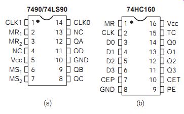
FIG. 6 (a) Pinout for 7490, and (b) pinout for 74HC160. Table 3
Use table for the 7490 type of ripple counter chip.
The counter is clocked by the trailing edge of the clock pulse. The maximum ripple delay, from the clock pulse input to the Q3 output, is in the order of 100 ns for standard TTL, but around 50 ns for the LS version of the chip.
For decade counting with synchronous counters we would normally make use of an integrated unit such as the 74HC160 type, whose pinout is shown in FIG. 6(b). This is not so simple as the 7490, considered earlier. To start with, this is a totally synchronous counter, and its internal flip-flops are triggered at the leading edge of the clock, with the outputs also changing at this time. The counter is fully pre-settable, meaning that the count number can be preset at any stage so that a count from, for example, 3 to 9 rather than 0 to 9 can be carried out if necessary. Only an up-count is available, and the counter allows a hold state in addition to its presetting state, making it fully programmable.
The MR input is a reset input that is active when taken low. Using an RC network to delay the rise of the MR input at power-up can reset the counter, before counting begins. This is often necessary because in any device that consists of a set of flip-flops, application of power will cause some flip-flops to set to a 1 output, while others to reset to a 0 output. In some applications a counter cannot therefore be used immediately power has been applied; it must be reset before any counting pulses are applied. The reset action, as usual, is completely asynchronous and this is reflected in the table by the X, which means 1 or 0 (the don't care state). The CP pin takes the clock pulse input, and the arrows in the table are a reminder that the changes take place on the leading (0 to 1) transition of the clock pulse, which should have a short rise time.
The CEP and CET inputs are normally high for counting, but taking either or both to level 0 will cause the count output to hold its existing state.
This action must not be used while the clock pulse input is low, only after the leading edge of the clock pulse when the clock input has settled to a high state. The PE pin is used for parallel loading of the flip-flops, allowing a number to be preset before counting starts or restarts. FIG. 7 shows a typical sequence of reset, load, count and hold (count inhibit) actions.
Parallel loading is enabled when the PE pin voltage is taken to 0, and in this state each Q output will take the state of its corresponding D input.
FIG. 8 shows a five-decade counter (to a count of 99999) which makes use of these units, connecting them together so that synchronous counting is preserved. Note that synchronous decade counters can be connected to each other in an asynchronous way, with the output of a counter driving the clock of the next, but the circuit shown here preserves fully synchronous action, using one counter to gate the following counters.
Suppose that we want to count in scales other than 8-4-2-1 binary or BCD. The gating methods that are used for synchronous counters allow for any counting system to be used, and design of the state machine is carried out making use of state tables to show what J and K entries are required, and diagrams called Karnaugh maps to show what gating can achieve this.
Karnaugh maps allow the designer to evaluate graphically the simplest representation of a function; however, in practice they have been largely superseded by computer-based design tools.
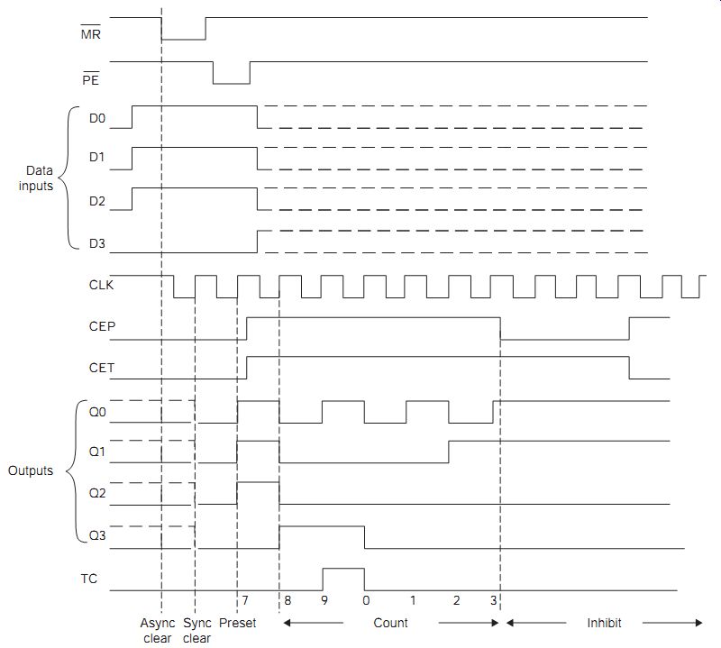
FIG. 7 Typical operating sequence of the 74160 counter, reset counter,
preset with 7, count, inhibit
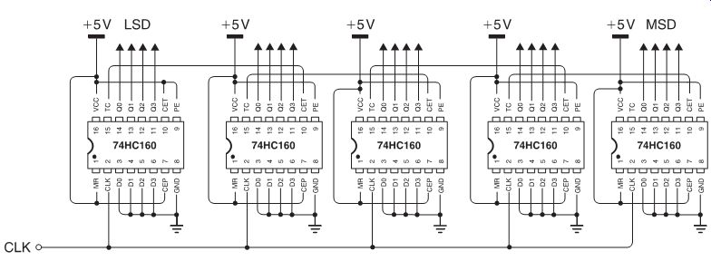
FIG. 8 Five-decade counter using 74HC160 chips, drawn as it might
be built.
A binary count can be achieved to any count number by repeating a basic design. This is not necessarily true of other types; using Karnaugh maps, a practical limit of four stages is reasonable. Typically, complex counting systems would be implemented in a microcontroller, application-specific integrated circuit (ASIC) or field programmable gate array (FPGA), and design software would be used to determine the required states and their implementation.
[ EXPERIMENT 2: Assemble and test modulo-n (where n is any whole number) counters, both synchronous and asynchronous. Use ICs such as 74LS74, 74LS112, 74LS193 and 74LS390.]
Shift registers
A register is formed by interconnecting a number of bi-stables in a similar way to a counter. Each bistable forms a memory cell for one bit of information. The data may be input in serial or parallel form and read out in a similar manner, depending on the method of interconnection. There are thus four basic forms of shift register:
• serial in, serial out (SISO)
• serial in, parallel out (SIPO)
• parallel in, parallel out (PIPO)
• parallel in, serial out (PISO).
Some IC implementations are shift registers of one form only, while others are more universal, with the mode of data transfers controlled by the logic values of separate control lines. The general principle is explained using FIG. 9, where a simple basic register is formed from D-type flip-flops (R-S flip-flops may also be used). Remember that the logic value on the D input is transferred to the Q output on the next clock pulse. In this example, each data value input thus ripples through the register in a manner similar to the counter.
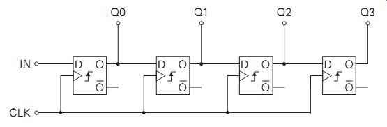
FIG. 9 Simple 4-bit shift register
The functions performed by shift registers include:
• multiplication and division (SISO)
• delay line (SISO)
• temporary data store or buffer (PIPO)
• data conversion; serial to parallel and vice versa (SIPO and PISO)
• serial input-parallel output shift register.
FIG. 10 shows the simplified internal schematic of the 74HC194, a universal version of a 4-bit shift register based on D-type flip-flops with AND-OR control logic. This provides for synchronous parallel data loading with serial and parallel output, and control of shift direction.
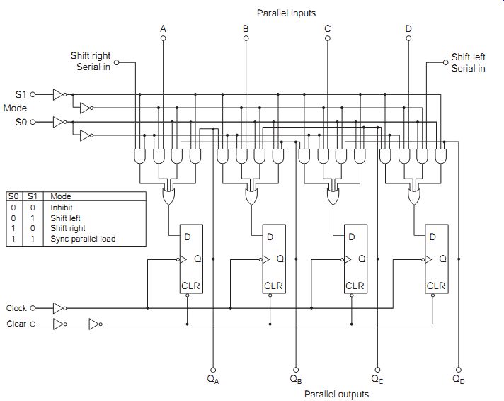
FIG. 10 Simplified schematic of the 74HC194 4-bit universal shift
register
The function of shift register is controlled by two mode select inputs S0 and S1, which determine the direction of shift and synchronous parallel load, or inhibit the shift register when both lines are low. The mode inputs drive a 4 to 1 multiplexer in each stage, consisting of four three-input AND gates and a four-input OR gate. This allows the state of the mode lines S0 and S1 to determine where the D input bit of the flip-flop comes from. With the S0 line set to logic 1 and the S1 line set to logic 0 the leftmost AND gate of each group is enabled. This carries the shift right bit to each stage.
Setting S0 and S1 both high selects the next AND gate, which enables the parallel input, so that on the next clock pulse the parallel input is synchronously latched. Similarly, when S0 is set low and S1 set high the third AND gate from the left of each group is enabled and the shift left bit passed to the D flip-flop. When both S0 and S1 are low, the rightmost AND gate is enabled and the output of the stage is fed back to its input, meaning that clock pulses do not cause any change in the register state.
[[ EXPERIMENT 3: Using ICs such as the 74HC194 (FIG. 11), assemble and test shift registers of each basic type. Once you have tried the various operations, use two shift registers to transfer parallel data via a serial link.
How many connections do you need between the two shift registers?
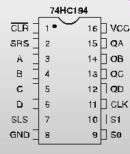
FIG. 11 Pinout of the 74HC194 4-bit universal shift register ]]
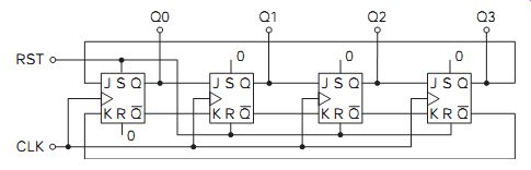
FIG. 12 Straight-ring counter circuit using a SIPO register. The
register must be set up with one 1 bit, since it cannot count if all outputs
are zero.
Ring counters
A shift register shifts the bits one place on each clock, so if a right shifting shift register is loaded with 1000 and clocked three times the result will be 0001. This assumes that it loads zeros to the LSB from the left. This can be viewed as counting in powers of 2; that is, it was loaded with 20 and after the first clock the output was 21, then 22 and finally 23 after three clocks. If the output of the last stage is fed back to the input of the first one, as illustrated in FIG. 12, it will cycle through these powers of two continuously.
FIG. 12 shows a set of four flip-flops connected in the usual Q to J, Q to K shift register mode, with a reset arrangement that resets all but the LSB flip-flop, setting a logic 1 into the LSB. After resetting, each clock pulse will then circulate that 1 by one place to the right and so back to the first flip-flop again. Such a counter can be very useful for sequencing because the other method of using a conventional binary counter and decoding logic requires many more gates to implement.
Ring counters can be set up to count arbitrary integer numbers of clock pulses. Simply by setting the number of stages, a seven-stage ring can be used to divide the clock signal by 7, giving a single high pulse out once for every seven clock pulses. Such counters can also be very much faster than conventional synchronous counters.
A disadvantage of the ring counter for dividing is that the output pulse is typically nothing like 50% duty cycle. One way around this problem, which also halves the number of flip-flops required, is to use a switch-tailed ring counter. As the name suggests, this is simply a ring counter with an inversion in the feedback (FIG. 13).
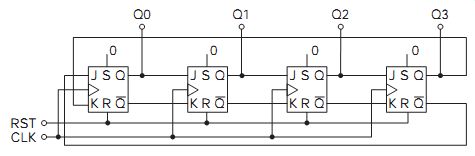
FIG. 13 Switch-tailed ring counter
The switch-tailed ring counter, also called the Johnson counter or twisted ring counter, has another advantage, in that the reset circuit is simpler: reset ting all the flip-flops is sufficient. FIG. 13 shows a four-stage counter, hence it is a mod-8 counter, the output going through one cycle for every eight input clocks.
The count of a Johnson counter is 2 x n, where n is the number of stages, rather than the 2n that can be achieved with true binary (8-4-2-1 or Gray)
counters. A four-stage Johnson counter will therefore give a scale of nine rather than the scale of 16 that a true binary counter can provide. The Johnson numbers always consist of a block of 1s and a block of 0s with no alternation of digits.
Ring counters of the type shown so far have a disadvantage that if, for some reason, whether a power glitch or other transient effect, they reach a number not in their designed sequence, they will count with the new pat tern without returning to the intended sequence, until reset. To avoid this lockout the feedback signal can be taken from the last two stages using an AND gate. This has the effect of removing patterns such as 101 from the sequence until the original sequence is recovered. A Johnson count for a four-stage counter is shown in Table 4 for the shift-register connections illustrated in FIG. 13.
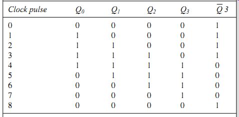
Table 4 Count table for four-stage Johnson counter
Apart from direct pulse counting, counter devices can perform many functions in industrial process control. Any transducer that can produce a pulse output can be used with a counter to automate an action on the basis of the number of counts received.
• Downward count: a downward count to zero is useful. This is used on some automatic coil-winding machines. The required number of turns to be wound on to a bobbin is first preset, and the machine set in motion. When the count reaches zero the machine automatically comes to a halt.
• Frequency: a counter can be used to measure the frequency of both unipolar ( d.c.) and bipolar (a.c.) waveforms by counting the number of cycles over a precisely controlled period. It can also be used to measure time if driven by a precisely known crystal frequency.
• Timekeeping: this is the basis of the digital watch or clock. In radar or sonar systems a transmitted pulse is reflected from an object and some of the energy returned to the source. The time delay can be measured and since the velocity of radio or sound waves is known, the time can be converted into distance.
• Velocity: two photocell/light source pairs can be set up a known fixed distance apart. The time taken for an object to pass between them can be measured and the distance/time computed to give the velocity.
Earlier, we saw that switches produce multiple output pulses, called con tact bounce, when switched. This is the reason for debouncing circuits.
[[ Experiment 4: Use a counter circuit and a switch without a debouncing circuit to show how many pulses that switch bounce causes. Try a variety of different switches. ]]
FIG. 14 shows a typical counting device designed to measure frequency. A crystal-controlled oscillator's output frequency is divided down to produce an accurate time gating signal. In practice, the frequency is chosen to be high enough to provide the maximum count or minimum time ranges to meet the user demand.
In the case shown, the crystal frequency is 32.768 kHz which, when divided by 215 , provides a time gate of 1 s. The input signal is converted into a square wave by a suitable circuit and then used to clock the counters. The displayed count then represents the unknown frequency in cycles per second or hertz.
This circuit uses several different types of counter that have been covered in the preceding pages. The oscillator and first divider is a single IC 74HC4060. This contains a divide by 2^14 ripple counter and provides a 2 Hz output to the 74HC4017, which is a mod-10 Johnson ring counter and is used to generate a sequence of control signals.
The COUNT signal is a 1 s wide positive pulse from the Q0 output of the 74HC4017, which enables the counters for exactly 1 s, in this case synchronous BCD counters. The Q2 output of the 74HC4017 is inverted to provide the active low LATCH signal for the 74HC4511 display drivers, which latches the count so that it can be displayed. The RESET signal is also inverted to drive the active low MR pin of the 74HC160 counter. The counters are reset ready for the next count, but the display continues to display the value that has been latched. The circuit updates once every 10 s, which is the time taken for the Johnson counter to go through a complete cycle.
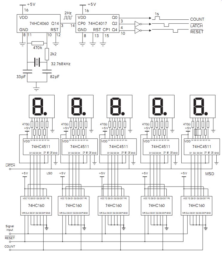
FIG. 14 Simple five-digit frequency counter circuit
QUIZ:
__1 How is a transparent latch different from a D-type flip-flop?
(a) it is edge triggered
(b) it is level triggered
(c) it does not have a preset input
(d) it does not have a Q output.
__2 How does the master-slave J-K flip-flop help in high-speed logic design?
(a) it minimizes propagation delay between stages
(b) J input connects directly to Q and K to Q of the previous stage
(c) is faster because it is clocked internally on both edges of the clock signal
(d) it avoids race conditions from the output to the input.
__3 Why should ripple counters be avoided in decoded applications?
(a) they are inefficient
(b) race conditions exist as the count ripples through (c) they count in binary only
(d) they use more stages to count than a Johnson counter.
__4 What sort of shift register can be used for converting parallel data to serial stream?
(a) SIPO
(b) SISO
(c) PISO
(d) FIFO.
__5 What is the main advantage of ring counters over binary ones when used as dividers?
(a) they can divide by arbitrary integer values more quickly
(b) they can be made from shift registers
(c) they can count up as well as down
(d) they have 50% duty cycle output