AMAZON multi-meters discounts AMAZON oscilloscope discounts
5. PRELIMINARY CONSIDERATIONS FOR ARTWORK CONSTRUCTION
In preparing to construct the artwork master, several considerations need to be noted to avoid improper tape arrangements. These considerations are:
1. A separate terminal pad must be provided, with its center on grid, for each component lead to be soldered to the conductor pattern. In cases in which large conductor areas are used instead of individual conductor pads, each component lead must still be provided with its own access hole.
2. Whenever possible, conductor paths should be along the vertical and horizontal lines of the grid system. However, irregular paths are acceptable only if they simplify the conductor pattern.
3. Attention should be focused on the conductor width and spacing. The cross-sectional area of the conductor path is determined in part by the amount of current it will be expected to handle. As discussed in Section 10, once the foil thickness has been selected, the minimum conductor width allowable is determined as outlined in Sec. 3 with the use of TABLE 7. Once this width has been established, the spacing between conductors must next be determined. TABLE 1 lists recommended conductor spacings for boards that will not be encapsulated (sealed) when completed. These spacings indicated are minimum for a wide range of ac or dc voltages and take into consideration the dielectric breakdown voltage characteristics. These characteristics refer to that voltage at which flashover (arc) among conductor paths occurs. For optimum circuit reliability, the components should be positioned in such a manner that the conductor width and spacing are not less than the minimums specified throughout the entire conductor pattern. In this phase of layout, the design must not be compromised. Once these minimum values have been determined, any reduction in either one for the purpose of preferred component repositioning for convenience or for the sake of appearance is unacceptable.
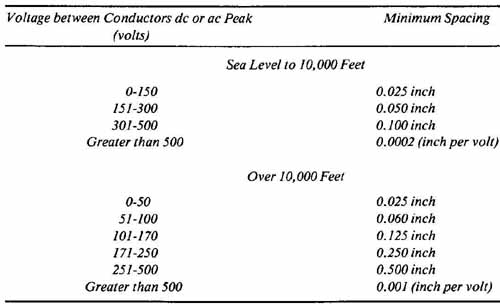
TABLE 1 Recommended Minimum Conductor Spacing
An example that illustrates the use of Tables 10.7 and 1 for the purpose of selecting an appropriate conductor width and spacing follows.
Example: Assume the following specifications:
Maximum continuous current: 1.6 amperes
Maximum voltage: 36 volts
TABLE 7 shows that a conductor width of 0.030 inch will safely handle 1.9 amperes using 1-ounce copper foil. This width allows an acceptable margin of safety. The spacing for the specified voltage requirements can be determined from TABLE 1, which shows that the minimum spacing for a 0- to 150-volt range is 0.025 inch. Therefore, no conductor path on the finished board can be closer to any other path than this minimum. The solution to this problem, therefore, is:
Conductor width: 0.03 1 inch
Conductor spacing: 0.025 inch
Notice that these specifications apply to the finished pc board. A 4: 1 taped artwork master would therefore employ 0.125-inch tape width with a minimum spacing between conductor paths of 0.100 inch. A 2: 1 taped artwork master would require a 0.062-inch tape width and 0.05-inch minimum spacing in order to achieve the desired results.
4. Finally, terminal area shapes and conductor path configurations must be evaluated so that only recommended artwork forms will be employed. FIG. 11 shows various terminal shapes and path layouts with the preferred pattern configurations, along with those that should be avoided. The use of those configurations that are not recommended may introduce problems such as undesirable voltage distribution along ground paths, nonuniform solder flow onto the conductor pattern (especially at terminal areas), and weakening of the foil bond.
6. TAPED ARTWORK CONSTRUCTION
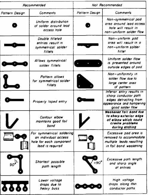
FIG. 11 Recommended pattern configurations.
To begin constructing the artwork master for a single-sided board, a sheet of polyester is placed over the component and conductor pattern drawings previously constructed and is firmly taped to the drawing board. This pad master will become the support for the taped artwork.
With a scalpel or other sharp instrument, the terminal pads (teardrops) are peeled from their protective paper backing and transferred to the polyester sheet. These aids should be positioned by using the underlying conductor pat tern drawing and centered with the aid of the grid system intercepts of the component layout. The entry of the teardrops should be oriented to align with their associated conductor path direction ( FIG. 12a). A single-entry teardrop will properly accommodate only one termination of a path with a filleted entry. If another conductor is terminated at the same terminal pad, it is necessary to provide an additional filleted entry. FIG. 12b shows an un-filleted conductor termination. FIG. 12c shows one method of obtaining a second filleted entry by overlapping two single-entry teardrops. When this method of filleting is used, tape buildup results. This is undesirable since it may yield poor line definition during the photographic reduction process. The preferred method is to use the proper double-entry teardrops, as shown in FIG. 12d. The technique of overlapping is necessary only if conductor path entry angles are other than 90 or 180 degrees apart. These angles are standard with the double-entry teardrops, as shown in FIG. 10.
FIG. 12 Methods of conductor filleting: (a) entry alignment; (b) unfilleted conductor entry; (c) both entries properly filleted by overlapping single-entry teardrops; (d) precut double-entry teardrops are preferred.
Complex device outlines, such as those for transistors, integrated circuits, or connector patterns, are next transferred to the pad master, as indicated by the component and conductor layout drawings. The positioning of these group units is accomplished by the technique shown in FIG. 13a and b. These group units must be firmly pressed into place once positioned to ensure that the entire adhesive backing makes positive contact with the surface of the pad master. The pad master for the complementary-symmetry amplifier board completed to this point is shown in FIG. 14.
With all device outlines and terminal pads properly positioned, the conductor paths can next be formed. The end of the tape is positioned to overlap the entry of the terminal pad and pressed firmly into place. As it is unrolled, the tape is guided along the conductor path and pressed down securely against the pad master until the desired termination point is reached ( FIG. 15a). The conductor layout and the grid system are used as guides for positioning the tape. The tape width should be positioned approximately over the single lines representing conductive paths on the component layout drawing viewed through the pad master. During this procedure, minor changes in tape direction or spacing can be made from the plan originally laid out in the component layout drawing if necessary ( FIG. 15b). A sufficient amount of tape should be unrolled to reach between termination points. Once the tape has been positioned and pressed into place, the index finger should be firmly run over the entire length of tape a second time to affix it securely to the pad master and to ensure an even surface. Once the second termination point is reached, the tape is cut. (Caution: Do not attempt to cut down through the tape with the scalpel. In stead, the blade is rested flat against the tape and positioned along the in tended cut. The tape is then pulled back over the blade edge. This technique is shown in FIG. 1 5c. This eliminates the possibility of cutting through both the tape and terminal pad, which would result in an open circuit in the conductor pattern at that point.)
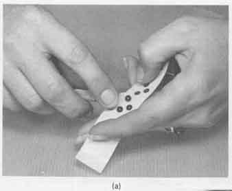
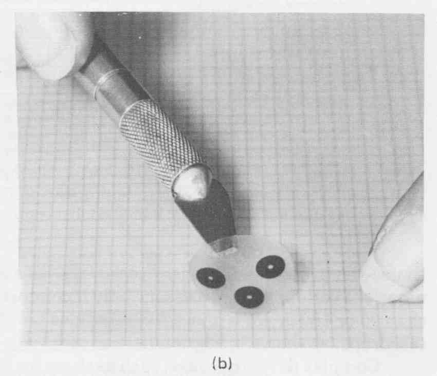
FIG. 13 Recommended method of positioning group units: (a) a knife
is used to re move unit from backing; (b) hold unit on blade to guide
into desired position. Courtesy of Bishop Graphics Inc., Westlake, Village,
Calif.
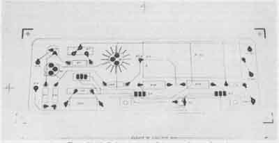
FIG. 14 Pad master with all device outlines and teardrops positioned.
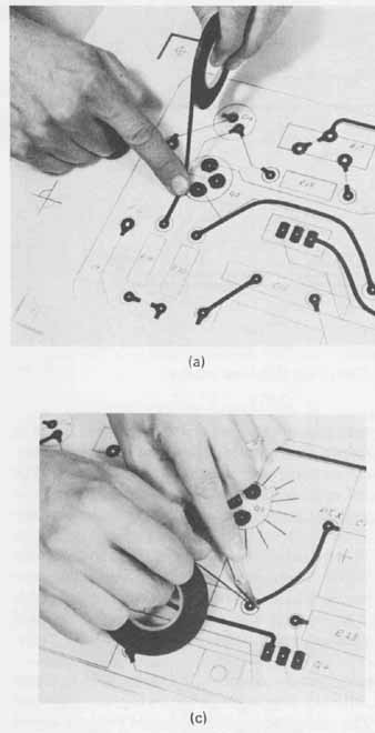
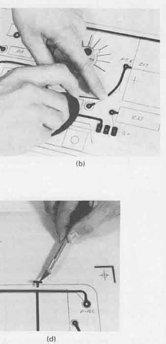
FIG. 15 Taping techniques: (a) tape should overlap teardrop entry;
(b) minor conductor repositioning for improved contour; (c) proper knife
placement for tape cutting; (d) tee to fillet conductors at right angles.
When a conductor path changes direction with a sweeping bend, the tape is formed to the desired contour by using the index finger of one hand to apply pressure and the other hand to uniformly guide the tape direction. When conductors intersect at right angles and fillets are desired, tees are positioned as shown in FIG. 15d. The pad master for the complementary. symmetry amplifier board with the conductor paths completed is shown in FIG. 16.
Upon completion of the conductor path taping, the routing should be checked with the schematic diagram to ensure that no errors have been made in the conductor patterns. These patterns must provide the exact electrical inter connections among the components as shown on the schematic diagram. The most efficient way to check the pad master with the schematic diagram is to have one technician read off the particular lead connections made by the conductor pattern and another technician check each corresponding connection on the schematic. A colored pencil aids in marking over the wiring and connections on the schematic as they are compared. These marks are essential in discovering errors in the pad master. Remember that any error not detected during this check will result in a corresponding error in the etched pattern. Continual checking for error through every phase of artwork development will ensure accurate results.
To complete the artwork master, border delineation marks, grid locators (targets) positioned in alignment with the points on the drawing, and artwork reduction dimensions are added. The completed artwork should contain keyed information if a marking mask is not to be used. (As will be seen later, a marking mask identifies completely all components on the insulated side of the board.) In addition, all components that might be positioned incorrectly on the pc board should be keyed similarly to the layout drawings. Finally, a descriptive identification number is positioned on the master.
Notice that all literal and numerical designations on FIG. 17 are reversed. The reason for this is that the original artwork master is generated fr7ii the component side of the board. Since a photographically reduced negative of this tape layout will be needed to process the foil side of the board, a physical reversal of this negative will be necessary, resulting in the proper orientation of literal and numerical designations as well as correct device lead and conductor patterns. FIG. 3 shows the foil side of the tone control circuit board being processed with the correct negative orientation. Reversed literal and numerical designations are available for keying pad masters generated from the component side of the pc board. An alternative and more economical method of keying is to apply dry transfers (discussed in Section 9) directly to the side of the pad master opposite to that of the taped conductor pattern.
The completed artwork masters for the amplifier’s power amplifier and power supply boards are shown in FIG.
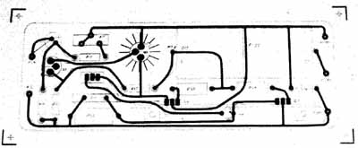
FIG. 16 Completed taped pad master.
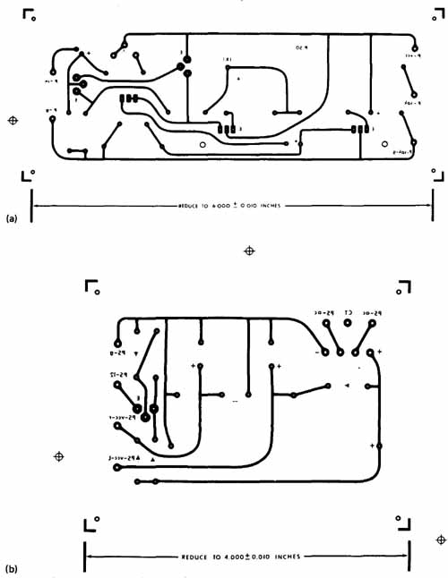
FIG. 17 Completed conductor pattern artwork masters: (a) power amplifier;
(b) power supply.
7. SILK-SCREEN SOLDER AND MARKING MASKS
The procedures and techniques thus far discussed for designing component lay outs, conductor pattern drawings, and pad master artwork represent the mini mum requirements for producing pc boards. To provide for more efficient soldering, a solder mask maybe employed.
FIG. 18 Power amplifier solder mask.
The artwork for the solder mask is prepared on a sheet of clear polyester taped to the pad master alone. Duplicate size solid donuts, as shown in FIG. 10, and device outlines are positioned on this polyester sheet directly over those areas on the underlying conductor pattern that will eventually be the soldered terminal pads on the processed board. Corresponding targets and board delineation marks must also be added to aid in all necessary artwork and board alignment. This solder mask artwork is a positive pad master.
To form the solder mask over a conductor pattern, a silk screen is necessary. The silk screen is prepared from a reduced negative of the positive pad master. The silk screen is then produced by using the techniques discussed briefly in Section 9 and to be considered in detail in Section 13. All the areas seen as clear on the positive solder mask artwork will be clear on the silk screen. The opaque terminal areas will be filled with the film gelatin when the screen is processed. The silk-screen solder mask must have the same reduction size as the conductor pattern artwork master. When the conductor side of the board is positioned under the silk screen, the application of an appropriate solder resist through the screen will coat all areas of the board, including the conductor pat tern with the resist except those terminal areas to be soldered.
The completed solder mask prepared from the power amplifier pad master is shown in FIG. Notice the targets positioned for alignment purposes.
The solder mask will protect the conductor side of the board during the soldering process. It is employed after the board has been etched. Only the ex posed terminal areas will allow solder to alloy with the conductor pattern and provide sound electrical and mechanical connections for component leads. A solder mask is utilized almost exclusively for automatic soldering methods such as dip and wave soldering (described in Section 15). Since only the terminal areas are exposed, less solder is required, thereby reducing weight and cost. Without the mask, the entire conductor pattern would be alloyed with the sol der.
A marking ask is employed to aid in component mask shows component outlines, positioning, and identification numbers. When processed into a silk screen, the mask will allow this information to be printed pc board. For the purpose of preparing marking masks, precut outlines of the type shown in FIG. 19 are used. To construct the marking mask, a piece of clear polyester is taped over the component lay out. With a scalpel, the component outlines are transferred to their appropriate positions. This procedure is shown in FIG. 20. Component identifications, such as R R C C Q etc., should be in accordance with the schematic diagram and are easily produced with the aid of dry transfers (see Section 9). The marking mask artwork’s grid locations and reduction scale should coincide with that of the master artwork.
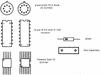
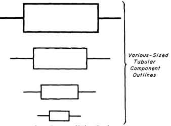
FIG. 19 Device and component outlines. Courtesy of Bishop Graphics,
Inc., Westlake Village, Calif.
The marking mask artwork is then processed into a silk screen with the screen becoming a negative marking mask. The application of a suitable epoxy paint will produce the desired information on the insulated side of the board. The completed marking mask for the power amplifier board is shown in FIG. 21. At this point, a differentiation between the information generated by a marking mask and the symbols produced from the conductor pattern pad master on the copper side of the pc board should be noted. As previously mentioned, the painted information on the insulated side of the board is used to simplify component assembly. The symbols on the foil side are for quick reference for testing purposes. However, as is often the case, the total information found on both sides of the board is helpful in identifying components and in rapidly locating test points.
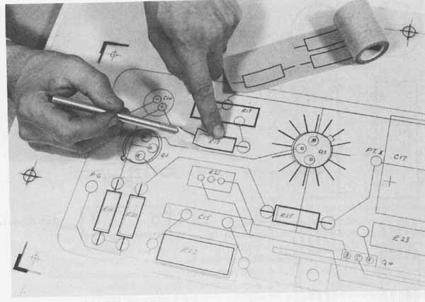
FIG. 20 Construction of marking mask pad master.
Because of the complexities and difficulties inherent in the design of printed circuits, a flow chart is provided in FIG. 22 to aid the technician by showing the logical sequence of procedures necessary to generate all the drawings and artwork for pc boards. Inspection of this flow chart will show that it is a complete sequential review of pc board design in outline form.
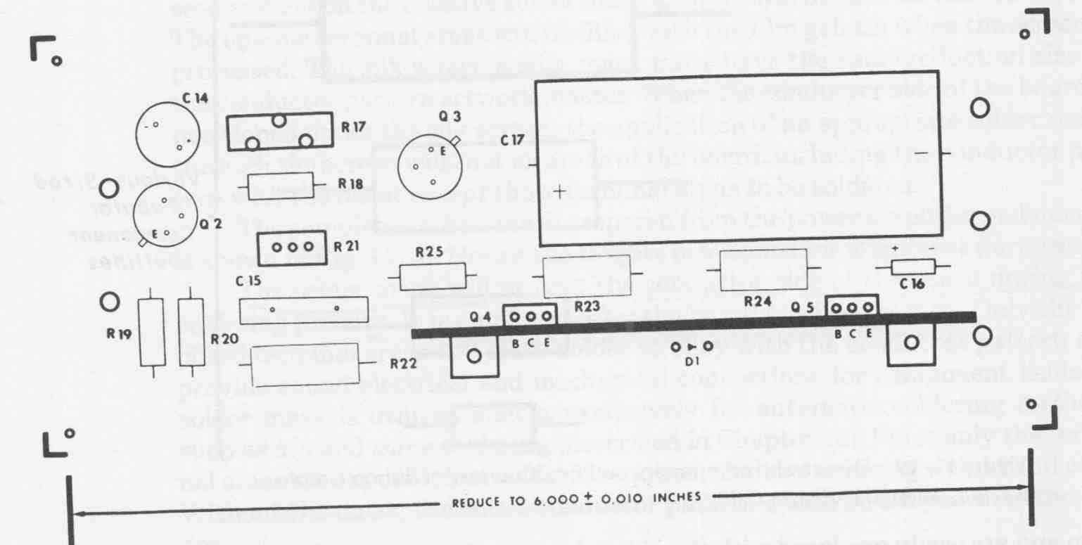
FIG. 21 Power amplifier marking mask.
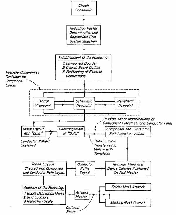
FIG. 22 Flow chart for printed Circuit layouts.
8. COMPUTER-AIDED DESIGN OF PRINTED CIRCUIT BOARDS
As electronic systems become more complex, there is a constant demand to package more parts into a smaller area, that is, to increase package density. This demand places more stringent requirements for narrower, more uniform conductor widths and spacings, smaller pad diameters and the accuracy of their positions, as well as closer layer-to-layer registration on both double-sided and multilayer designs.
As a result of these requirements, which place a high priority on quality at a faster production time, the move is away from manually taped artworks and toward the more accurate and rapid computer-aided design (CAD) systems. CAD systems are divided into two broad categories. The first type is the high- end workstation that supports large industry. This type consists of a dedicated minicomputer with large mass storage (memory) and high-speed processing capability and is used in conjunction with powerful CAD software packages. The second category of CAD systems is built around the popular personal computers and utilizes compatible software.
The basic building blocks of a typical CAD system consist of a computer (mini or personal) with a color monitor, a keyboard and/or mouse digitizer as an input peripheral, and a printer or plotter as an output peripheral. This hardware, together with an appropriate CAD software package, form a complete design system.
The design of a pc board begins with the design of the circuit schematic. From a library of standard electronic symbols, available in memory as part of the CAD software, the operator calls up a part, locates it on the monitor, and provides it with a reference designator (e.g., R All of the component and part symbols are called up, in turn, and positioned, labeled, and properly interconnected. This continues until the circuit schematic is complete, including all de tailed information such as pin identifications.
A net list is next generated by the CAD software from the completed circuit schematic. The net list is a detailed listing of all component interconnections derived from the circuit schematic. At this point, a hard-copy net list, a circuit schematic, and a parts list can be produced if required.
The CAD software package also includes a footprint library in which is stored the part or device body outlines, normally viewed from the component side, as well as terminal pad configurations. From this library, the operator calls up a part and positions its footprint within the board outline displayed on the monitor. This parts placement phase may be done solely by the operator or with the aid of the parts positioning program available in some software pack ages. The operator can interact with this program, stopping it when it is deemed necessary, and use his or her skills to optimize parts placement.
With all the parts in place, a check routine is run to compare all the parts with the net list generated previously. This check ensures that there are no parts missing or incorrect parts used.
The next phase in CAD layout is conductor path routing. This can be accomplished manually by the operator who positions the individual conductor paths together with their width and spacing as dictated by the circuit schematic and board requirements. Also available are various autorouter software programs which run as part of the CAD package. A typical approach to routing conductor paths is to use an autorouter software routine in conjunction with operator interaction. This interactive approach usually results in an optimum path layout.
The type of autorouting software selection depends on the type of boards to be designed. Simple double-sided circuits with moderate packaging densities can be brought to within 90 to 95% of completion with most autorouting pack ages that run on personal computers. These software packages are best suited for digital circuits. The 5 to 10% of the traces that the software package is un able to complete must be completed by the operator.
More complex designs, having high-density component packaging in double-sided or four-layer multilayer boards, require a maze type of autorouter if high completion rates are to be realized. Surface-mounted technology, discussed in Section 21, has resulted in extremely dense boards that require high-performance rip-up-type routers, which are best suited for high-end work station CAD systems. The layout shown in FIG. 23 was generated by a CAD system.
With all conductor paths completed, several check and verification routines are run. The conductor path design is first checked to confirm its agreement with the circuit schematic. In this way, any missing or incorrectly routed paths will be identified. Design specifications, such as conductor width and spacing, are then verified.
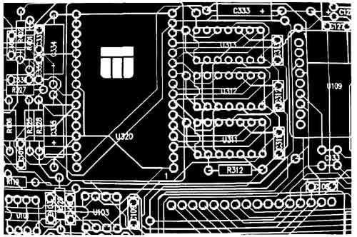
FIG. 23 CAD systems layout.
With the layout and checks completed, all the data is stored in memory. From this data, an entire document package can be developed. The minimum documents that any software package provides are the plots for each artwork layer. Then, depending on the type of software used, more documents can be generated. These include solder masks, component marking masks, assembly drawings, drill tapes, router tapes, and automatic insertion tapes.
With the generation of the vast amount of information available from the data base developed in the design phase, CAD systems have increased the quality of pc boards while reducing costs and decreasing turnaround time.
The next Section is devoted exclusively to the photographic processes required in producing a pc board from the drawings and artwork masters developed in this Section.
EXERCISES
A. Questions
1 For what reasons are artwork masters produced larger than actual size?
2 Explain the overlay method used for artwork master construction and state an advantage of this procedure.
3 What are grid locators used for, and how are they positioned?
4 What do corner brackets define?
5 What is a pad master, and how is it constructed?
6 What is the purpose of a solder mask?
7 What two types of drafting aids are used in the preparation of component layout drawings?
8 Why is the spacing between conductor paths a critical specification?
9 What is the purpose of a marking mask?
10 What feature in a CAD software package aids in parts positioning?
11 How much larger are the lead access hole diameters made for component assembly by automatic insertion than for manual insertion?
B. True or False
Choose T if the statement is true or F if any part of the statement is false.
1 Artwork masters should be constructed to a 1 : 1 scale to maintain required tolerances. T F
2 For 2: 1 scale reductions, 0.100-inch grid systems are standard. T F
3 The component border defines the location of the edges of the overall printed circuit board. T F
4 Conductor paths must not be drawn through component body outlines. T F
5 The component and conductor pattern layout allows both sides of the pc board to be viewed simultaneously. T F
6 Grid locators are positioned inside the board delineation marks. T F
7 A separate terminal pad must be provided for each component lead to be soldered to the conductor pattern. T F
8 The solder mask artwork is a negative pad master. T F
9 The width of the conductor path is determined by the amount of current it is to carry. F
10 The net list generated by a CAD software package provides component body outlines for ease in pc board layout. T F
11 Designing a pc board for automatic assembly uses the same criteria as those for manual component assembly. T F
C. Multiple Choice
Circle the correct answer for each statement.
1 Whenever possible, artwork masters should be constructed (two, four) times larger than actual size to maintain tolerances.
2 A 0.005-inch-thick Mylar grid system will exhibit a dimensional stability of ( ± 0.02 inch, ± 0.002 inch) in 48 inches.
3 The overall board outline is delineated by (corner brackets, grid locators) on an artwork master.
4 Literal and numerical designations are (right, reverse, reading on the foil side of a single-sided layout viewed from the component side.
5 The minimum spacing for a voltage of 150 volts dc between conductors at sea level is (a 0.125 inch, 0.025 inch).
6 Component body o programmed in a CAD software package are referred to as (net list, footprints).
D. Matching Columns
Match each item in column A to the most appropriate item in column B.
COLUMN A | COLUMN B
1. Precut component outlines 2. Donuts 3. Grid systems 4. Solder mask 5. Corner brackets 6. Keying 7. Teardrop |
a. Silk-screen artwork b. Overall board outline c. +, —, E, pin 1 d. 0.1-, 0.125-inch spacings e. Dolls f. Terminal pads g. Double entry |
E. Problems
1 Using the appropriate templates and poster paper, trace and cut 2: 1 and 4: 1 scale drafting aids (dolls) for all resistor and capacitor sizes determined and tabulated for Problem 3.4. Also construct dolls for transistors, diodes, and integrated circuits of the 8- and 10-pin TO-5 style, and the 14- and 16-pin dual-in-line configurations with reference to FIG. 3b.
FIG. 24
2 Referring to the 14-pin dual-in-line test jig configuration shown in FIG. 24, construct the test jig conductor pattern drawings to a 1: 1 scale and tape the artwork masters for the 8-pin TO-5, 16-pin dual-in-line, and TO-86 flatpack configurations. The conductor pattern for the TO-86 flatpack test jig is to be designed for soldered finger connections requiring the double 90-degree bend configuration shown in Fig. 14.27c. Each printed circuit board for the test jigs must be no larger than 3 by 4 inches. The pc boards are fabricated in Problem 13.2. Drilling terminal pads and installing terminal socket pins are performed in Problem 14.2. Tinning of the conductor pattern and soldering of terminals and socket pins are done in Problem 15.2. A test jig stand is constructed in Problem 23.4.
3 Draw the component layout and conductor pattern to a 2: 1 scale for the circuit diagram shown in FIG. 25a. This circuit is a seven-fixed- interval UJT timer. The pin arrangement of the timer selector switch used in this circuit and shown in FIG. 25b is identical to that of the 14-pin dual-in-line integrated circuits shown in Appendix II. L S and the battery are to be chassis-mounted. External connections may be made to any board edge. The component layout design must be confined within a 2 by 4 border. Choose a suitable chassis, indicating lamp, and battery and battery clip styles for the design. An optional design may be considered that uses individual chassis-mounted time-interval selector switches. The seven time intervals for the circuit range from approximately 5 to 35 seconds. The pc board is fabricated in Problem 13.4 and assembled and soldered in Problems 14.3 and 15.3, respectively. Installation of the pc board into the chassis fabricated in Problem 8.5, along with the mounting of the on-off switch, indicating lamp, and battery clip, is accomplished in Problem 23.5. All interconnections among the chassis-mounted components and hardware and the pc board are soldered in Problem 24.5.
Time Selector Switch (See FIG. 28 b)
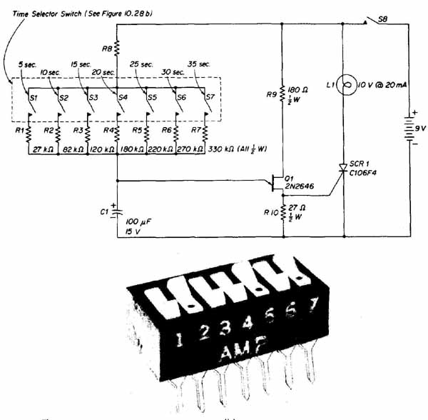
FIG. 25
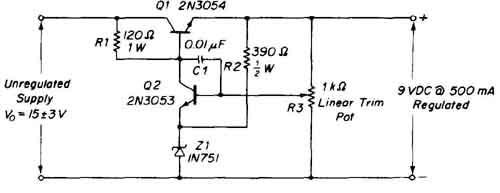
FIG. 26
4 Construct a 4: 1 scale component layout and conductor pattern for the series feedback regulator circuit shown in FIG. 26. All input and out put connections are to be located on one edge of the pc board and de signed for finger-type connection. The maximum size of the pc board is to be 3 by 3 inches. The printed circuit is fabricated in Problem 13.5 with component assembly and soldering performed in Problems 14.4 and 15.4, respectively.
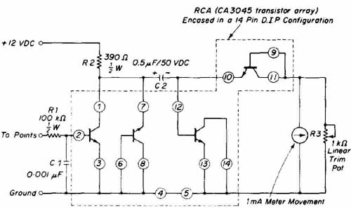
FIG. 27
5 Design 2: 1 scale component and conductor pattern layouts for the tachometer circuit given in FIG. 27. Maximum pc board size is to be 1 by 2 inches with provision for a suitable pc connector on one of the 2-inch sides of the board. Construct 2: 1 artwork masters and marking and solder mask layouts for this design. All components and external connections are to be identified and keyed where necessary. The silk screens are constructed in Problem 13.3 and employed in Problem 13.6. Printed circuit board component assembly and soldering are undertaken in Problems 14.5 and 15.5, respectively. The pc board and meter are mounted in Problem 23.6. The harness for interconnections is constructed in Problem 24.6. An optional double-sided circuit design may be considered for this problem.