AMAZON multi-meters discounts AMAZON oscilloscope discounts
<< cont. from part 1
5. HAND SOLDERING PRINTED CIRCUIT BOARDS
Of prime importance in soldering is that the surfaces to be joined are clean and void of oxides. For pc board soldering, this is especially true, for a poorly cleaned terminal area would prolong heating time excessively when soldering, which could upset the foil bond. The terminals should not only be cleaned but it is imperative that liquid flux be applied to all joints prior to soldering even if terminal areas have been tinned. The flux may be applied to the pc board by any of the methods discussed in Sec. 2. However, wiping is preferable in prototype work when a solder mask is to be employed, such as in the case of the amplifier’s pc boards. This method allows the flux to be selectively applied only to those terminal areas that are to be soldered. The pc board is first secured in a circuit board holder and tilted to a horizontal position. Liquid flux is then applied with a fine artist’s brush or toothpick onto the areas to be soldered.
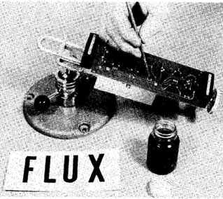
FIG. 6 Applying flux to PCB
This arrangement is shown in FIG. 6 for applying flux to the power supply board. When all the surfaces to be soldered have been coated with flux, soldering may begin.
To solder leads to pc boards, it is important that heat and solder be applied quickly and accurately. A small amount of solder is initially applied to the flat of the soldering iron tip (solder bridge) to promote rapid heat transfer to the joint ( FIG. 7a). The entire flat of the tip surface is then placed in contact with the terminal area and lead simultaneously. The more surface area of the tip contacting the terminal pad and lead, the more efficient the transfer of heat ( FIG. 7b). The joint is allowed to heat to the melting point of solder, usually taking from 1 to 2 seconds for most connections. Solder is then applied to the terminal pad and lead simultaneously and at a point on the opposite side of the lead from where the tip is contacting. The correct orientation of tip and solder is shown in FIG. 7c. As soon as the solder begins to flow, no more should b applied. Since solder follows heat flow, it will wet the entire connection and flow over the lead, forming a smooth contour of solder around the lead and terminal pad. The soldering iron is then removed and the joint allowed to cool. The joint must never be moved until the solder has completely solidified because an movement of the lead as it is cooling will prevent positive alloying from taking place. It is important to apply only a minimum amount of solder sufficient to ensure proper alloying. A properly formed solder joint is smooth and shiny in appearance. All surfaces must be completely wetted and the contour of the lead on the terminal pad clearly visible. A correctly soldered lead to a printed circuit terminal pad is shown in FIG. 8. A precaution should be mentioned here. When soldering the individual terminal pads, it is important to keep track of those leads that must be heat-sinked. Lead heat sinking is discussed in Sec. 14.4.
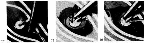
FIG. 7 Printed circuit board soldering: (a) forming a solder bridge;
(b) heating solder pad and lead; (c) solder application.
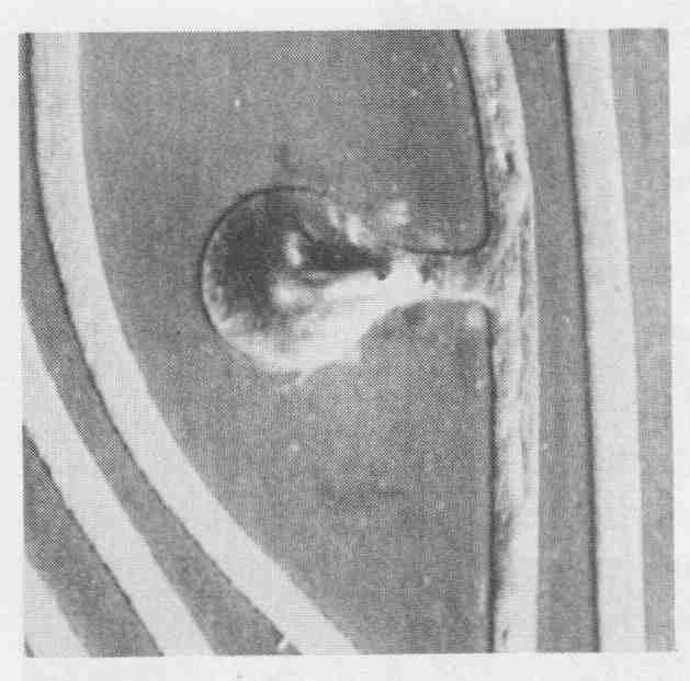
FIG. 8 Correctly soldered terminal.
Excess solder and contaminated flux residue on a tip must be removed before another solder joint is formed. Cleaning is accomplished quickly and easily by wiping the tip on a moist sponge. Soldering should never be attempted with a tip covered with excess solder or contaminants if quality results are to be expected.
Swaged terminals are soldered to pc boards in a similar manner to lead soldering, with one important exception. Since the terminal pad area for swaged terminals is larger than those used for lead connections, it is necessary to apply heat for a longer period of time. The flat area of the soldering tip is placed in contact with the swaged portion of the terminal and solder is applied to the terminal pad. When heated sufficiently the solder will completely wet the terminal pad and flow uniformly around the swaged terminal in the area where it contacts the copper foil.
Since many pc boards do not employ solder masks, and if conductor pat tern plating is not economically feasible, the technician may wish to tin the en tire conductor area of the board to retard oxidation. This can be done during the soldering operation. Flux is first applied to the entire board surface. A small amount of solder is applied to the flat of the tip and the tip is slowly drawn along the conductor path. A thin layer of solder will be deposited on the surface of the copper. Several passes may be necessary to completely tin a conductor path. This will prevent excessive solder from forming in addition to minimizing foil bond damage. For this technique, a soldering iron with a tip temperature of between 500 to 600°F (260 to 316°C) should be used. The application of solder via the soldering tip is restricted to tinning conductor patterns. This technique is never employed for making soldered connections.
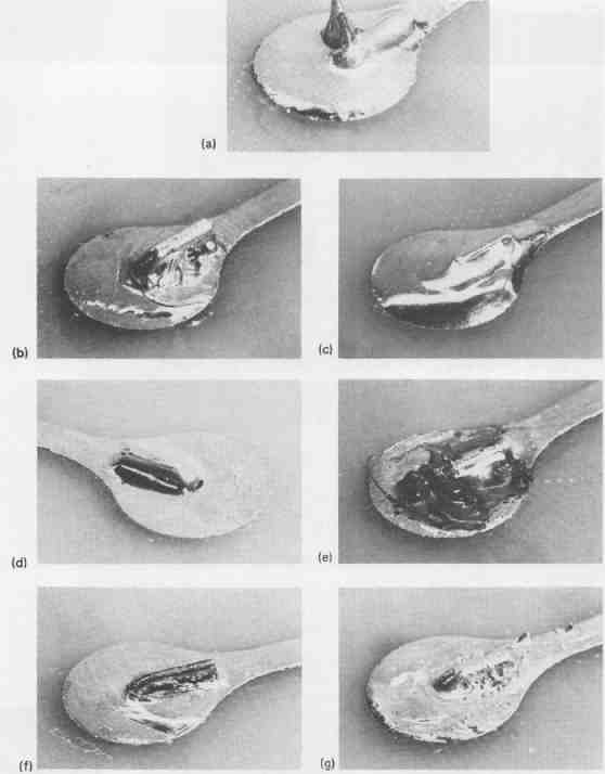
FIG. 9 Typical inferior solder connections: (a) solder peaking; (b)
incomplete wetting; (c) excessive solder; (d) cold solder joint; (e)
rosin joint; (1) fractured joint; (g) porous joint.
Properly soldered connections are uniform in appearance and their quality may be judged by visual inspection. Each solder joint may be inspected immediately upon soldering or after completion of the entire board. To aid in this inspection, a 5 x to 10 x magnifying glass may be used. Following is a list of deficiencies and their causes common to improperly soldered connections. These are shown in FIG. 9.
1. Solder peaking: characterized by a sharp point of solder protruding from a connection. Peaking is caused by the rapid removal of heat before the entire joint has had an opportunity to completely reach its soldering temperature. The solder follows the hot tip as it is removed from the connection, resulting in this peaking condition. Reheating the joint will correct this deficiency.
2. Incomplete wetting: occurs when portions of the soldered connections have not been alloyed with solder and are completely visible. This may be the result of both insufficient heat and solder. It may also be the result of contaminants on the soldering tip or terminal pad. Reheating the joint and applying additional solder will correct this fault if the condition is not caused by contaminants. In that case, de-soldering and cleaning are necessary before a new joint is attempted. The terminal pad can be cleaned with a sharpened pencil-style typewriter eraser. (De-soldering techniques are discussed in Sec. 15.6.)
3. Excessive solder: evident when the lead contour is not plainly visible. This is extremely undesirable since it prevents complete inspection of the alloying action of the solder, thus obscuring potential troubles. This condition can be rectified by removing some of the solder with the use of desoldering aids.
4. Cold solder joint: an inferior connection easily detected by its dull-gray, grainy appearance, or as a cluster of solder that has not properly wetted all the surfaces. This is the result of applying insufficient heat, which pre vents solder from alloying with the metal parts. Cold solder joints can generally be corrected by reheating the connections. If, however, the puddling of solder is caused by a connection that has not been thoroughly cleaned, it must be de-soldered and cleaned before it can be properly soldered.
5. Rosin joint: a joint in which a layer of flux residue is formed between the terminal pad and the solder. Since flux is an insulator, this condition could result in electrical discontinuity between the lead and the terminal pad. Rosin joints are the result of too short a heating time. The soldering iron tip must remain on the connection for a short time after the applied solder is withdrawn. This allows proper wetting action and causes all the flux to float to the surface with the captured oxides. This defect can be corrected by reapplying heat.
6. Fractured joint: characterized by the appearance of minute cracks in the solder. These cracks appear if the lead is moved before the solder has had an opportunity to completely solidify. This may be corrected by the reap plying of heat, if the lead will not again be moved during the cooling period. This problem of component and lead movement arises when a pc board is soldered with the components resting on a work surface. It is preferable to clamp the board by its edges in a circuit board holder, such as that shown in FIG. 6.
7. Porous joint: characterized by pinhole imperfections visible in the surface of the solder which is due to trapped gases caused by insufficient heating time, a period required to allow volatizing flux to escape. This fault can be remedied by reheating.
Flux residue remaining on the connection after soldering is undesirable. This residue presents a poor board appearance and contaminants suspended in this residue could cause troublesome electrical leakage paths. If more active fluxes must be used, their removal is doubly important to prevent corrosion. Flux removal can be accomplished by hand brushing, dipping, or with ultra sonic equipment.
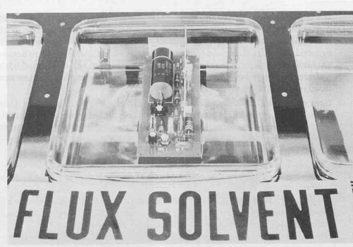
FIG. 10 Mild agitation for flux removal is accomplished by use of a rocker table.
Brushing with a stiff-bristle brush dipped in a flux solvent is often accept able but may not remove flux completely from inaccessible cavities characteristic of pc boards in which swaged eyelets and terminals are used. Dipping and mildly agitating the board in a solvent bath is preferable since it will improve solvent action in some areas that are not possible to reach by hand brushing ( FIG. 10). A more efficient means of flux residue removal, especially when activated fluxes are used, is to use an ultrasonic tank containing the flux solvent. Several minutes in this system ensures the most thorough cleaning.
FIG. 11 Hand-soldered amplifier boards.
For most electronic soldering applications, rosin flux residue is the type most generally encountered. Alcohol and trichiorethylene are excellent solvents for this residue. As in the case of most solvents, certain hazards present themselves. Alcohol is flammable and trichiorethylene should be used in a well ventilated area and kept away from the skin. Finally, the remaining solvent are quickly evaporated by the use of an oil- and moisture-free air hose. The seven pc boards for the amplifier, hand-soldered and using the techniques discussed in this section, are shown complete and ready for assembly to the main chassis in FIG. 11.
6. DE-SOLDERING PRINTED CIRCUIT BOARDS
When a lead is soldered to a terminal pad, it is difficult to remove without damaging the component or the terminal area. Several commercially available desoldering aids, however, simplify this task. These aids are the solder which desoldering bulb, solder sucker, dc-soldering tips, and extraction tools.
A solder wick is made of finely woven strands of tinned copper wire such as that used for shielding coaxial cable (see Section 24). This flattened wick is first dipped into a liquid flux to promote solderability. It is then placed over the terminal area and lead to be dc-soldered. This arrangement is shown in FIG. 12a. The soldering iron tip is placed in contact with the solder wick and pressed down against the connection. As the heat from the iron is transferred to the wick and connection, the solder will melt and flow in the direction of the heat transfer. The solder is thus trapped by the solder wick as it flows up through the weave. The result is shown in FIG. 12b. The solder can be completely removed from the joint with this method. The used portion of the wick is discarded. Solder wick is available in rolls for many dc-soldering applications. With the solder removed from the connection, the lead can be bent away from the terminal pad and the component easily withdrawn.
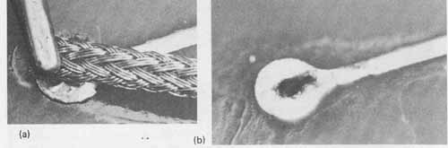
FIG. 12 DC-soldering technique employing solder wick: al position of
solder wick and soldering tip; (b) dc-soldered terminal pad.
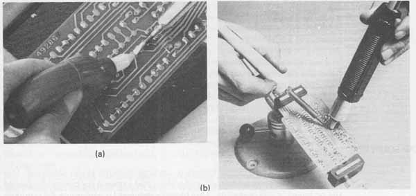
FIG. 13 DC-soldering equipment (a) dc-soldering bulb, courtesy of Ungar
Division of Eldon Industries, Inc.;(b) solder sucker.
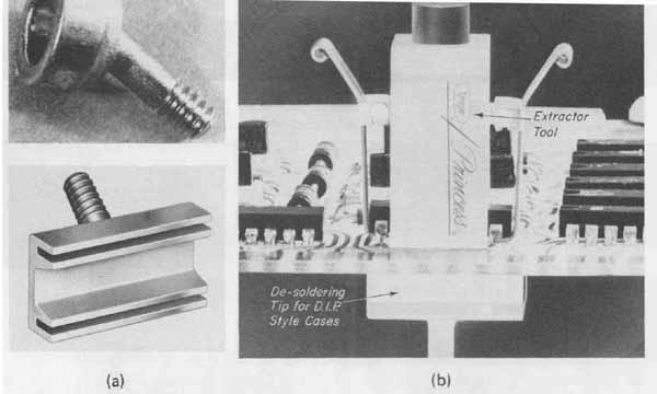
FIG. 14 Device de-soldering equipment: (a) de-soldering tips for TO-5
and DIP-style cases; (b) de-soldering DIP-style devices. Courtesy of
Ungar, Division of Eldon Industries, Inc.
The dc-soldering bulb and solder sucker, shown in FIG. 13, can also be used for removing excess solder or for dc-soldering component leads. Both tools have hollow Teflon tips with high heat resistance and will not scratch or mar delicate pc board conductors. The dc-soldering bulb, shown in FIG. 13a, is employed by depressing the bulb and then placing the hollow tip alongside the soldering iron tip on the joint. As the solder begins to melt, the bulb pressure is released. The liquid solder is drawn up into the bulb by the suction. Both tools are then removed from the connection for inspection. If solder remains, the process must be repeated. The solder-sucker shown in FIG. 13b is employed in basically the same manner except that the suction is produced by a spring-loaded piston. The piston handle is first pushed downward. The handle is then rotated to engage the release pin. As the solder begins to melt, the pin is disengaged and the solder is drawn up through the hollow tip as the piston snaps upward inside the tubular handle. Both tools are easily disassembled to remove the accumulated solder. These de-soldering tools do not generally remove sufficient solder on the first attempt to allow components to be removed, thus rendering the solder wick the preferable method.
For removing ICs, the previously discussed de-soldering aids would have to be used on each lead individually, making it a time-consuming process. De soldering tips specifically designed to simultaneously heat all the leads for removing devices quickly and easily are available for this purpose. De-soldering iron tips for TO cases and dual-in-line configuration ICs are shown in FIG. 14a.
The de-soldering tip is placed in contact with all the device leads simultaneously. As the leads are de-soldered from the foil side of the board, the device is removed from the component side with an extraction tool such as that shown in FIG. 1 4b. With this tool, the device is lifted away as the solder is melted. The remaining solder present on the terminal pad may obstruct the access holes and can be removed with any of the de-soldering aids discussed. The recommended type of extraction tool is one whose metal clamps grip the leads, thus providing some degree of heat sinking. It must be mentioned that lead heat sinking is just as important when de-soldering as it is during soldering to avoid damage.
7. DIP SOLDERING
One method of soldering pc boards in mass production is dip soldering. Dip soldering completely solders all connections and exposed copper conductors of the pc board in one operation. This process requires (1) solder pot (2) temperature control unit, (3) bar solder, (4) dross removal tool, (5) board holder, and (6) flux applicator. After the flux is applied to the conductor side, the board is floated on the surface of molten solder. An even coating of solder will be deposited onto the entire surface of the conductor pattern. Although this process appears basically simple, the preparation and implementation are somewhat involved.
The preparation of the surfaces to be soldered is critical if quality results are to be realized. Absolute cleanliness is essential. The use of solder masks presents the fewest problems in dip soldering since the exposed areas to be soldered are small and the possibility of solder bridging is eliminated. (Solder bridging is the undesired formation of solder between conductor paths.) Flux is applied to the surface just prior to soldering even if the conductor pattern has been tinned.
Flux may be applied, as previously mentioned, by either dipping, wiping, sponging, or spraying. The object is to apply a uniform layer of flux over the entire surface of the board. This layer should be kept to a minimum thickness to promote improved solderability. If excessive flux is applied, it will not completely decompose at temperatures below those of molten solder, resulting in the formation of gas pockets between the board and the surface of the solder. These gas pockets will cause an uneven wetting of solder. Because of these limitations, wiping with a brush is the most effective way of applying flux onto the board. When the flux has been applied, the board must be soldered immediately.
The specified tin-lead ratio for dip soldering is normally 60/40, which melts at approximately 370°F (188°C). Placing a pc board onto the surface of the molten solder will lower the solder’s temperature. Consequently, a guard temperature must be included to allow for this cooling. A guard temperature of between 50 and 70°F (10 to 21°C) is normally sufficient. This means that the solder pot temperature should be maintained between 420 and 440°F (216 to 227 °C) and accurately controlled. Although higher temperatures will hasten soldering, problems such as board warping and strain effects on the foil bond will be encountered. The exact temperature for optimum results for any particular system is best determined by trial and inspection.
As the solder pot is operated at elevated temperatures (above 370°F or 188°C), an oxidizing scum, referred to as dross, will form on the surface of the molten solder. If not removed, this dross will adhere to the areas to be soldered, resulting in cold solder joints. Just prior to floating the board onto the solder, the dross must be removed. This can be done by skimming the surface with a piece of aluminum mounted to an insulated handle ( FIG. 15a).
The board is placed in the pot and held firmly along its edges with tongs equipped with insulated handles. First one end of the board is lowered in direct contact with the solder at an angle of approximately 45 degrees with the surface. This procedure is shown in FIG. 15b. The board is then slowly tilted downward until the entire conductor pattern surface is contacting the molten solder. This technique of slowly tilting the board will force any gases generated during the flux decomposition period to escape from between the solder and board surface. With the board in complete contact with the surface of the solder, it is moved about the pot ( FIG. 15c) to allow uncontaminated solder to continually contact the conductor pattern. The soldering operation should take from 4 to 7 seconds, depending on the solder temperature and type and amount of flux used.
After the board has been allowed to remain in contact with the solder for the prescribed amount of time, it is slowly raised to a 45-degree angle before it is completely removed from the pot. This technique is intended to reduce the possibility of the formation of solder peaks (points of solder protruding from the conductor pattern). Visual inspection should be made to ensure that no solder bridges between closely spaced conductors have formed. Although solder cannot alloy with the insulating material, bridges may still form between closely spaced conductors. The resulting appearance should be a completely wetted conductor surface with a smooth, uniform coating of solder. Once the flux residues are removed, the board is completed. A properly soldered single- sided pc board is shown in FIG. 15d.
Dip soldering, owing to its reasonable setup costs, can be adapted equally well to prototype applications. However, the results are not uniformly consistent or predictable. Often, hand-soldering touch-up work may be necessary to achieve quality results.
Extreme caution must be exercised when dip soldering. This process requires continual safety precautions because of the ever-present danger inherent when working with molten metal. Protective glasses, gloves, and an apron should be worn to guard against solder splatter. Although a pronounced “sizzling” sound will be heard when the cool surface of the board first contacts the solder surface, this is normal and should not cause concern. This effect is the result of the rapid volatilization of the flux. To prevent serious personal injury from a violent solder eruption, all liquids should be kept away from the solder pot.
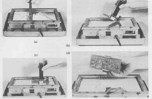
FIG. 15 Sequential method for dip soldering: (a) dross removal; (b)
initial board-entry angle; (c) board is moved about solder surface; (d)
soldered conductor pattern.
8. WAVE SOLDERING
A much more elaborate system of production line pc board soldering that eliminates many of the inconsistencies resulting from manual dip soldering is the process of wave soldering. This method is widely used in the industry because of its large soldering capacity, its ability to accurately regulate time and temperature exposure of the pc board, the scrubbing action of the solder wave which aids in complete wetting and soldering of each joint area, and the consistently high-quality results obtained.
A typical wave-soldering system consists of three main sections. These are the fluxer, pre-heater, and solder wave. An integral part of the system is a conveyor which is used to accurately control the movement of the pc board over the fluxer, the pre-heater, and the solder wave. Pre-cleaning and post-cleaning cycles of the pc board are not a part of the system and are performed separately.
A typical bench-type wave-soldering machine is shown in FIG. 16. The conveyor speed is adjustable from 1 to 15 feet per minute at angles of between 5 and 9 degrees with the surface of the bench. The board is introduced into the system by attaching it to the fingers of the conveyor. The circuit side is first run across a foam fluxer. At this station, a head of fine bubbles rise from the fluxer. These bubbles are typically generated by passing air through a sub merged porous ceramic cylinder that is impervious to the flux. A chimney and brushes aid in uniform flux distribution. The bursting flux bubbles rise by capillary action and penetrate into plated-through holes. Rosin-based flux, such as Kenco No. 465 Resin Flux, having 25% or higher rosin content, is generally preferred in the wave-soldering process. This flux not only promotes uniform solder wetting and formation of a strong intermetallic bond with the copper, but it also reduces the surface tension of the liquid solder. Surface tension reduction is important in preventing solder bridges and icicles (solder peaks) from forming.
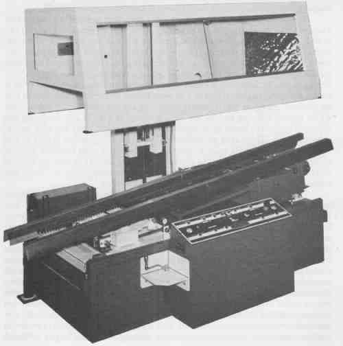
FIG. 16 Bench-type wave-soldering machine. Courtesy of the John
Treiber Company.
After the board is fluxed, the conveyor continues its travel over a pre heater station. The purpose of this station is threefold. First, preheating evaporates excess flux solvent on the board to prevent splattering and entrapped gases which could cause pinholes in connections when the board is soldered. Second, it conditions the board and assembly against thermal shock. Third, preheating the board helps to overcome the heat-sink effects on large components caused by the solder wave. Preheaters must be capable of providing a range of heat, as measured on the component side of the board, from 100 to 275°F (38 to 135°C). Overheating the flux must be avoided because it degrades its effectiveness by reducing its mobility.
With the board preheated, it is next conveyed over the solder wave, which quickly produces large numbers of high-quality and well-contoured solder connections simultaneously. These connections are both electrically and mechanically sound. The wave is formed by pumping molten eutectic solder (63/37) vertically upward through a solder nozzle having a large plenum chamber that rests in a solder pot. A high-capacity centrifugal pump propels the molten solder through the nozzle to form a standing wave. The most commonly used wave shape is bidirectional, that is, solder flows in two directions.
Bridges and icicles will usually result if the solder system has too narrow a solder wave and the boards are run on a horizontal conveyor (see FIG. 17a). A web of solder tends to extend beyond the wave in the direction of travel, which creates these problems. If the solder wave is narrow, inclining the conveyor to an angle of 5 to 9 degrees will increase solder peel back and therefore reduce the solder web and significantly reduce solder defects (see FIG. 17b). For best results, however, a solder system having a deep, wide wave (3 to 4 inches along the path of travel at 1 or more inches above the nozzle edges) and an inclined conveyor will virtually eliminate the formation of a solder web which causes bridging and icicles. This is shown in FIG. 17c. Inclining the conveyor causes the board to be introduced onto the solder wave at a high solder- velocity point. This takes advantage of the natural scrubbing action of the wave at this point in its velocity profile. A wider wave used together with an inclined conveyor also allows the soldered conductor pattern to exit the wave at a practically zero velocity point which not only increases solder peel back but reduces heat transfer to the components being soldered.
To obtain the smoothest solder wave and result in minimum solder deposits having a bright, shiny appearance, the formation of dross (oxides of tin and lead) must be kept to an absolute minimum. One method of reducing the dross formation is to use an oil (soldering fluid) as a dross blanket in the solder pot. As solder is pumped, the oil forms a thin film on the surface of the wave. An other effective method is to intermix oil, such as Hollis No. 225 Soldering Fluid, by precision metering with the wave at the impeller of the pump. This causes the oil to disperse uniformly within the solder wave. In both methods, the oil reacts with the dross to form harmless tin and lead soaps without degrading the solder. In addition, the surface tension of the solder is reduced which allows excess solder to drain more easily from the board. The soldered boards also become coated with the oil, which intermixes with the rosin flux and protects the soldered connections from oxidation. This mixture of oil and rosin is easier to remove than rosin alone in the cleaning process, assuring bright soldered joints.
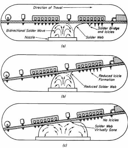
FIG. 17 Use of wide solder wave with oil and an inclined conveyor eliminates
solder bridges and icicles; (a) narrow solder wave with horizontal conveyor;
(b) narrow solder wave with inclined conveyor; (c) wide solder wave with
inclined conveyor.
Although wave soldering is an automated process, a degree of skill and knowledge of soldering is necessary to properly operate the system. This knowledge includes an understanding of the proper conveyor speed, type of flux, pre-heater temperature, width of the solder wave, solder temperature, the use of an oil blanket or oil intermix, and the established quality standards. When the pc boards have been assembled, soldered, and cleaned, they may be tested for operational performance and modifications made if necessary.
9. THERMAL PROFILE OF THE WAVE SOLDERING PROCESS
One essential function of a process engineer may be to evaluate and modify a wave soldering system in order to quantify both the magnitude and duration of temperatures that contact a pc board as it passes through the various operations. By tightly controlling the thermal profile of this process, high-quality results, with minimum rejects, will be obtained. The data acquisition system described in Sec. 4 is ideally suited to evaluate the thermal characteristics of a pc board as it passes through the wave soldering system.
Typically, during the wave soldering process, a pc board will be subjected to a temperature variation of from about 25°C (room temperature) to as much as 2500 C. For this reason, a type J thermocouple is selected and constructed by twisting and welding together iron and a constantan (40% nickel and 60% copper alloy) wire. This thermocouple is capable of accurately and repeatably measuring temperatures from —184 to + 760°C.
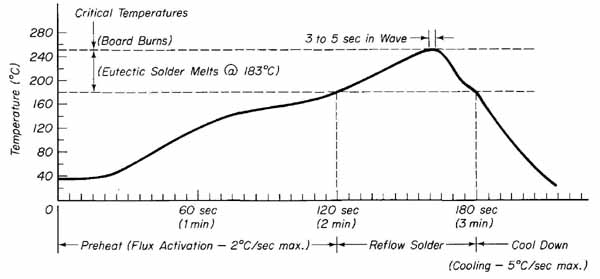
FIG. 18 Thermal profile of a conventional wave soldering process.
The thermocouple is first inserted into a small via hole of the board. (Refer to Sec. 16.1 for a description of a via hole.) The thermocouple must enter from the component side and should extend into the hole until it just begins to exit the circuit side. This arrangement will allow the temperature changes to be monitored and will simulate those changes to which a component lead would be subjected. The thermocouple extension leads pass above the component side of the board and to the input of the 6B11 signal conditioning module discussed in Sec. 4.
A thermal profile of a conventional wave soldering process obtained from the data acquisition system is shown in FIG. 18. Test panels are used to properly establish process parameters as follows: During the preheat or flux activation phase, a thermal rise of approximately 2°C/second is obtained by adjusting the conveyor speed within the typical range of 6 to 8 feet per minute. Optimum results are achieved when the circuit side surface temperature is about 183 °C, the melting point of eutectic solder, as the board exits the pre heater. As the board moves over the solder wave, additional heat is transferred to the board, which raises the circuit side surface temperature still higher. The board dwells in the molten solder wave for 3 to 5 seconds, causing the surface temperature to reach a maximum temperature of about 250°C. Control of the time that the board remains in the wave is a function of the profile of the wave and the depth to which the board extends into the solder. Refer to FIG. 18. Test panels can be run and rerun to adjust the controls for optimum results.
Finally, a maximum cool-down cycle of —5°C/second is recommended to minimize thermal shock and maximize joint strength.
The data acquisition system just described can be configured quickly with a personal computer and a menu-driven software package such as ACQUIRE, which is discussed in Sec. 15.4.
EXERCISES
A. Questions
1 What are the two metals used to make solder, and what is the percent age of each in solder used for general-purpose electronic work?
2 Explain the term eutectic solder. What is its melting point tempera ture?
3 What type of flux is used for electronic work?
4 What is the purpose of flux?
5 What is the recommended method of cleaning a plated soldering iron tip?
6 What is the approximate temperature of a 3/4-inch-long tip having a diameter of 3/64-inch when used with a 25-watt heating element.
7 Explain the following terms: cold solder, solder peak, and wetting.
8 What is used to remove rosin flux residue from electrical connections?
9 What benefits can be derived from the generation of a thermal profile for a wave soldering process?
10 What is solder wick used for?
11 What is the major cause of solder bridge and icicle formations when wave soldering pc boards? How is this eliminated?
B. True or False
Circle T if the statement is true, or F if any part of the statement is false.
1 Solder is an alloy of tin and lead. T F
2 For most hand-soldering applications, 60/40 eutectic solder is used. T F
3 Solder melts at a lower temperature than either pure tin or pure lead. T F
4 Rosin flux with activating agents is noncorrosive at room temperature. T F
5 Conical soldering iron tips are used when large areas must be rapidly heated. T F
6 When hand soldering, the solder should be placed between the iron’s tip and the lead to ensure proper wetting. T F
7 A cold solder joint can be corrected by simply reheating the connection without the addition of more solder. T F
8 A rosin joint is the result of allowing the lead to move prior to the solder solidifying. T F
9 In dip soldering, the board is removed from the molten solder at a 45-degree angle to reduce the formation of solder peaks. T F
10 Oil is used to reduce the formation of dross in a wave-soldering system. T F
C. Multiple Choice
Circle the correct answer for each statement.
1 Solder used in the electronics industry for component assembly consists chiefly of tin and (copper, lead).
2 Chloride-based fluxes are not used in the electronics industry because they are (expensive, corrosive).
3 Rosin-based fluxes are most active at (room, high) temperature.
4 For a constant soldering iron wattage rating, the tip temperature (in creases, decreases) as the tip length increases.
5 A good solder joint results if a (libera4 minimum) amount of solder is applied to the connection.
6 After a solder joint has been completed, flux residue is removed with the use of a solvent such as (alcoho4 hydrochloric acid).
7 A typical dip soldering sequence takes about (7, 40) seconds.
8 The most common method used by industry for soldering large quantities of pc boards is (dip, wave) soldering.
D. Matching Columns
Match each item in column A to the most appropriate item in column B.
COLUMN A | COLUMN B
1. Dross 2. Eutectic 3. Recovery time 4. Flux 5. Rosin joint 6. Solder wick 7. Alcohol |
a. Solder defect b. Return to idle temperature c. Flux solvent d. Rosin e. Oxidizing scum f. 63/37 ratio g. Desoldering tool |
1. Lay out, shear, and bend an aluminum tray for holding a soldering iron tip cleaning sponge. The tray is to have inside dimensions of inch by 3 inches by 3 inches. Tabs are not required on the inside corners. These corners are sealed in Problem 23.3 to retain excess moisture. Break all sharp edges with the appropriate file.
2. Dip or hand solder the printed circuit device test jigs that were designed and fabricated in Problems 11.2, 13.2, and 14.2. The entire conductor pat tern is to be tinned and all device pin locations numerically identified with dry transfers. A stand for mounting the test jigs is designed and constructed in Problem 23.4.
3. Solder the assembled pc board for the seven-fixed-interval UJT timer designed and fabricated in Problems 11.3, 13.4, and 14.3. Chassis mounting and interconnection wiring are done in Problems 23.5 and 24.5, respectively.
4. Solder the pc board for the series feedback regulator designed and constructed in Problems 11.4, 13.5, and 14.4.
5. Solder the pc board for the tachometer circuit designed and constructed in Problems 11.5, 13.6, and 14.5. Circuit board and meter installation are accomplished in Problem 23.6. Wiring is done in Problem 24.6.
---- --