AMAZON multi-meters discounts AMAZON oscilloscope discounts
LEARNING OBJECTIVES:
Upon completion of this section on artwork design and layout of double-sided plated-through-hole printed circuit boards, the student should be able to:
1. Understand the basic differences between single- and double-sided plated- through-hole pc boards.
2. Lay out double-sided pc boards.
3. Develop a color-coding system to distinguish conductor patterns on both sides of a double-sided pc board.
4. Be familiar with the three methods used in preparing double-sided layouts.
5. Prepare pad masters for double-sided designs.
6. Prepare taped artwork masters for both sides of a double-sided pc board.
7. Construct double-sided layouts with uniform distribution of patterns on both sides for optimum plating.
8. Produce diazo phototools for proper double-sided registration.
9. Use a densitometer on processed films.
0. INTRODUCTION
As electronic systems have become more complex, the requirements of higher- density packaging have partially been met with the widespread use of double sided printed circuit boards and the rapidly growing importance of multilayer pc boards (see Section 20).
Double-sided board fabrication requires the preparation of at least two pad masters, one for each side of the pc board. This, of course, adds to the time and costs of producing a double-sided board. Precise alignment of all terminal pads between both sides of the board is required for each lead access hole. This alignment problem is not a consideration in the preparation of single-sided boards since there is only one conductor pattern on one side of the board. In addition, double-sided boards require many more steps in fabrication which increases their cost as compared to single-sided boards.
Even though they are more costly and time-consuming to fabricate, double-sided pc boards allow for more components to be packaged in less space than single-sided boards and thus meet the demands for high-density electronic packaging.
1. BASIC DOUBLE-SIDED PRINTED CIRCUIT BOARDS
A double-sided pc board differs from a single-sided board in that both sides are processed with conductor patterns and terminal pads. The arrangement of conductor paths and pairs of terminal pads to form a double-sided pc board is shown in FIG. 1. As with single-sided boards, all components are mounted only on one side. This side is called the component side or top. Component leads pass through previously drilled and plated lead-access holes which have been processed through each pair of terminal pads on either side of the board. The component lead is clinched or bent over onto the terminal pad that is on the circuit side or bottom of the board. Note in FIG. 1 that the lead access hole drilled for the component lead also passes through a terminal pad on the component side of the board. Unlike single-sided designs, conductor paths may extend away from terminal pads on both sides of the board. Electrical interconnections between conductors on both sides of the board are made with plated- through holes (PTH) which become an integral part of the overall conductor pattern in the fabrication process.
When it is required only to make an interconnection between both sides of a double-sided pc board, a via hole is used. Also referred to as feed-throughs, via holes are not intended to accept component leads. For this reason, the terminal pads and drill hole sizes are small. Typically, a via hole pad size has a finished diameter of 0.050 inch with a drill hole size of 0.030 inch. The top and side view of a via hole would appear identical to that shown in FIG. 1 without the component lead and in Fig. 20.3 for a multilayer board.
The electrical interconnections between both sides of a pc board are formed by first drilling all lead-access holes in the bulk stock. Through a series of processes in chemical baths, all these holes are then plated with copper to form a continuous electrical connection between the copper surfaces of both sides of the board. Each copper surface is then imaged with the intended conductor pattern design. Further chemical processes result in additional copper and then solder to be plated on all the drilled hole walls. These processes, as well as those required to complete a double-sided plated-through-hole pc board, are discussed in detail in sections 17, 18, and 19.
The circuit side of the board can be considered a conventional single-sided layout. The conductors and terminal pads on the component side serve to extend the amount of conductor path routing. With both sides of the board used to route electrical interconnections, less space is required for conductor paths on the bottom side, thus allowing for greater component density.
One of the considerations involved in the fabrication of a double-sided pc board is the component bodies that must rest on the conductor paths which are on the top of the board. Most component and device cases, such as resistors, capacitors, plastic-cased transistors, and integrated circuits, are electrically insulated from their leads. The bodies of these components may safely contact a conductor path without electrical interference. However, some metal-cased integrated circuits and transistors have one lead attached to the case. These packages must not be allowed to come into contact with any of the conductor paths on the top side of the pc board. Electrical contact is avoided by either mounting these components slightly above the board surface to create an insulating air gap or with the use of one of a variety of plastic insulating spacers, some of which are shown in Fig. 14.21.
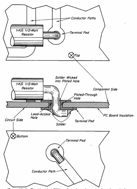
FIG. 1 DOUBLE-SIDED PTH pc board conductor board and terminal pad arrangement.
2. DOUBLE-SIDED COMPONENT LAYOUTS
The generation of a component and conductor pattern layout for a double-sided pc board is initiated in a similar manner to that for a single-sided board, that is, with the selection of a suitable grid system and reduction scale. The selection criteria for a double-sided pc board is the same for a single-sided pc board, as detailed in Sec. 11.1. These selection criteria will not be repeated here. however, it should be emphasized again that a 4: 1 scale layout on a 0.100-inch grid system should be used whenever possible.
For purposes of developing optimum component placement, it must be decided which of the three approaches—the schematic, central, or peripheral viewpoints—shall be employed. These component placement approaches are detailed in Sec. 11.2. One advantage of a double-sided pc board layout is that it allows more flexibility in path routing because of the use of both sides of the board for this purpose. Thus, some of the major path-routing difficulties en countered in single-sided layout are largely overcome.
When drawing the composite view of component and conductor pattern layouts, lines representing conductor paths on the opposite side of the board may “cross” each other. Because the conductor routing paths on both sides of the board are drawn as a composite view, a system to avoid confusion and mis interpretation must be utilized. A color-coded system for this purpose has been adopted by much of the industry. When viewing the pc board from the top (component side), the components are first seen. Below the components, again on the top side of the board, are the conductor paths and terminal pads unique to that side. Still viewing the pc board from the top, the conductor pattern on the bottom of the pc board would be “seen” as though one were looking through the insulating material. While laying out a double-sided pc board on a single sheet of grid paper, each side must be distinguishable. Adopting the fol lowing color-coded system will, to a large extent, eliminate confusion:
1. The outlines of all component bodies are drawn in black lead pencil.
2. All items that are common to both sides of the board are also drawn in black lead pencil. These items are typically:
a. Donuts (or teardrops) ---requiring drill holes
b. Special device outlines ---requiring drill holes
c. Mounting holes ---requiring drill holes
d. Corner brackets
e. Reduction scale
3. All conductor paths for the component or top side should be drawn in red pencil. All literal and numerical information and component keying should be done in red pencil and right-reading if it is to appear in copper on this side of the board.
4. All conductor paths for the circuit or bottom side should be drawn in blue lead pencil. All literal and numerical information and component keying should be done in blue pencil and reverse-reading if it is to appear right-reading in copper on the bottom side of the board.
The use of a color system allows three levels of views to be drawn onto a single sheet of grid system without confusion. For example, a blue conductor trace crossing a red conductor trace does not produce an electrical connection, since each color represents conductor paths on opposite sides of the pc board which are insulated by the board material. The color-coding technique outlined is illustrated in FIG. 2. Because of the absence of colored illustrations in this book, blue traces are shown as dashed lines and the red traces as solid lines to distinguish between paths appearing on opposite sides of the board. Figure 16.2 utilizes a basic transistor amplifier circuit to illustrate this double-sided layout technique.
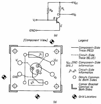
FIG. 2 Double-sided path layout coding: (a) basic transistor amplifier
circuit; (b) component layout showing composite of top and bottom views.
Before beginning the discussion of the preparation of the taped artwork master for double-sided pc boards, several important points must be emphasized. The objective of double-sided layout is to produce a taped artwork master for each side of the board with perfect registration of all pairs of donuts on both sides of the board. The donuts should be positioned on grid with the specified drill hole locations as found on the component and conductor pattern layout drawing. This is necessary to prevent misalignment of drill holes and pad centers on either side of the fabricated board. Figure 3 shows that the annular ring (amount of copper that will appear between the edge of a drilled hole and the outside edge of a copper pad) is dependent upon the accuracy of donut-pair alignment at each drill hole location. Where there are few drill holes and they are small relative to the terminal and diameter (i.e., large annular ring), this perfect registration problem is less severe when compared to the more complex designs with extremely small annular rings required by high-density pc board packaging. High-density packaging demands that all the available space on a pc board be used as efficiently as possible. In addition, the IC patterns used extensively have very small terminal pad areas, owing to the fact that their on-center spacing is typically 0.1 inch. It can be seen that achieving perfect top to bottom registration requires more care as the packaging becomes more dense.
There are three popular methods used in the preparation of double-sided taped artwork masters. These methods are:
1. Single-acetate with color system ( FIG. 4)
2. Two-acetate system ( FIG. 5)
3. Three-acetate system or donut master technique ( FIG. 6)
3. DOUBLE-SIDED TAPED ARTWORK MASTER CONSTRUCTION TECHNIQUES
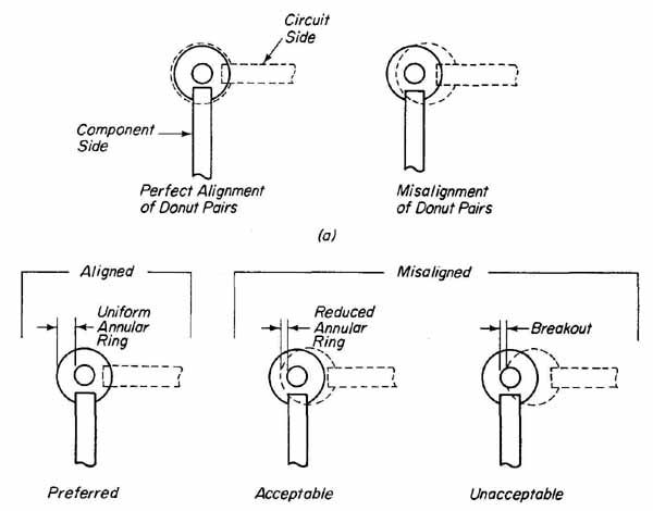
FIG. 3 Perfectly aligned donut pairs on the master artwork are required
to prevent misalignment of images on drilled panels. (a) Front-to- back
alignment of donut pairs; (b) donut alignment criteria for acceptability.
Each of these systems will be discussed together with their advantages and disadvantages.
The single-acetate color system, shown in FIG. 4, requires only one layer of acetate to which both sides of the double-sided pattern will be constructed. A single sheet of acetate is taped over the component and conductor pattern layout drawing onto the drafting board. Similar to all three layout systems, the drafting aids used to represent copper pads are solid having no lead-access hole. In addition, the special solid pad layout patterns, such as those for ICs and transistors, are used. These aids are laid out in black on one side of the acetate sheet. The purpose of the solid terminal pad is to blank out the entire pad area, including the drilled holes. The conductor pattern on the component side is constructed with the use of red polyvinyl tape which is rigid and transparent. This tape will not bend or stretch and therefore changes in path direction cannot be made by contouring the tape. Changes in direction are made with the use of a variety of special precut angle corners. By splicing between the tape and angled corners, the desired changes in path direction may be achieved. An alternative method of changing path directions without the use of precut elbows is to cut and splice the tapes by overlapping to the desired angle. It can be seen that layout with the colored tapes is more time-consuming than artwork constructed of flexible black crepe tape which can easily be contoured. In addition, the cost of the colored tapes is higher than that for the black tape.
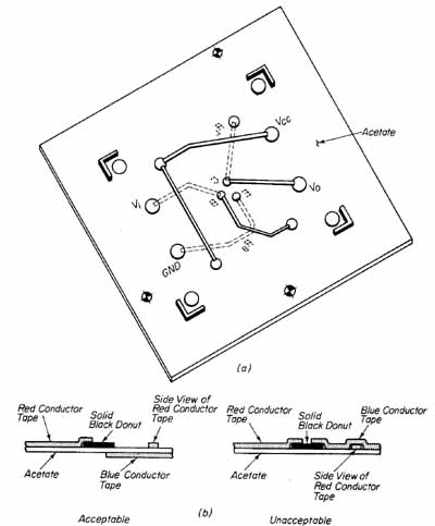
FIG. 4 Single acetate red/blue color system: (a) taped artwork for
Fig. 2, transistor amplifier (b) side view of acetate sheet with acceptable
and unacceptable taping techniques.
The conductor side is next constructed using blue tape. If this construction is to be made on the same side of the acetate as the component side, a problem will result where the blue tape must necessarily overlap the red tape. In the photographic reduction process, the areas where blue overlaps red results in a reduction of path width of the pattern in that area. This becomes more of a problem when extremely narrow tape is used. To overcome this problem, the blue taping should be done on the opposite side of the acetate sheet. However, this creates other concerns in construction. In order to place the blue tape on the opposite side, the acetate sheet must be removed from the component lay out drawing and reversed. This causes a problem of alignment, since the component layout drawings were made from the component view. To overcome this alignment problem, a mirror image of the component layout drawing is required for correct orientation.
Another problem that arises with the use of the single-acetate colored tape system is in the photographic process. A special blue filter must be attached to the camera, resulting in all blue lines being filtered out. Only red and black patterns will appear on the negative produced. Orthochromatic film, which can be processed in red safe light, is used for this purpose. To produce a negative showing the blue traces and black donuts, a red filter replaces the blue filter. With the use of panchromatic film, the red images are dropped and only the blue and black patterns appear on the negative. The use of panchromatic film greatly complicates the developing process, since this film must be processed in absolute darkness. In the absence of automated film processing equipment, developing time becomes a matter of many trials and errors. To overcome this, some graphic art tape manufacturers provide an amber/magenta color system to replace the red/blue system. This allows the total use of orthochromatic film in conjunction with a suitable filter system.
Through the use of the single-acetate color system technique, perfect alignment of artwork and resulting positive or negative phototools can be realized since only one set of donuts is used for both sides of the board. However, the added costs of materials and the disadvantages discussed above render this technique the least cost-effective of the three listed.
The two-acetate system, shown in FIG. 5, makes use of black crepe tape and solid black donut and device patterns. As a result, no special lens filters or special film types are required for photographic processing. The fact that the two-acetate system is an extension of the single-acetate system will become apparent in the following discussion.
A single sheet of acetate is taped over the component and conductor pat tern layout drawing onto the drafting board. All solid donuts and special terminal pad designs are first laid out. If this sheet is to be used to produce the artwork master for the circuit side of the pc board, all connections drawn in blue pencil would be routed using black tape with appropriate overlapping onto donuts and device pads. Finally, corner brackets, reduction scale, targets, component keying, and reverse-reading literal and numerical information is added to complete the conductor side layout.
To produce the component-side artwork master, a second acetate sheet is taped over the completed circuit-side layout. The most critical phase of this process is the registration between the two artwork masters. All solid donuts and special device patterns must again be installed on this second acetate sheet with extreme care that they are aligned with those on the conductor-side lay out. The placement of the donuts can be aligned easily with a reasonable degree of care. The alignment of the IC patterns, however, is much more difficult be cause there could be as many as 64 centers (64-pin DIP patterns) which must be simultaneously positioned exactly over the same style pattern on the conductor-side layout. The more special IC patterns involved in the layout, the greater possibility of pattern misalignment.
The component artwork master is completed with the installation of the conductor-path taping for all the red paths appearing on the component layout drawing and with the addition of corner brackets, reduction scale, targets, and numerical and literal information in a right-reading orientation.
This system is highly prone to misalignment, especially if extreme care is not exercised in firmly taping each configuration into its proper position. The two-acetate system is suitable for relatively low density packaging, in which few critical alignment situations are encountered.
A preferred method of preparing double-sided pc board artwork masters is the three-acetate or pad master system illustrated in FIG. 6. The pad master, which includes all solid donuts and special device patterns, corner brackets, mounting holes, targets, and the reduction scale, is produced first. Since all the items that are common to both sides of the pc board are installed onto the pad master, they will not appear on the other acetate sheets, resulting in no expensive duplication of materials, less time required for layout, and no alignment problems.
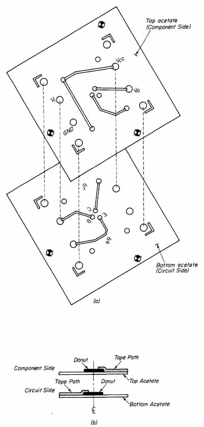
FIG. 5 Two-acetate taping system for double-sided layout: (a) separate
top and bottom taped artworks for the transistor amplifier; (b) side
view of taped artworks showing correct donut alignment.
On a second sheet of acetate, items unique to the circuit side are laid out. These include conductor paths drawn in blue pencil on the layout drawing and numerical information. The pad master aligned with the circuit-side taped master completes the composite artwork for the bottom side of the pc board.
On a third sheet of acetate, all items unique to the component side are laid out. Taping is provided for all red path traces on the component layout drawing in addition to the numerical and literal information. This layout, aligned with the pad master, completes the composite artwork for the top side of the pc board. Because the same pad master is used to produce both sides of the pc board, perfect alignment between donut pairs for both sides is easily achieved.
FIG. 6 Three-acetate taping system for double-sided layout: (a) separate
top, pad master, and bottom tapings for the transistor amplifier; (b)
side view showing correct tape overlapping with donut and path alignments.
4. PAD MASTER FOR THE PREAMPLIFIER CIRCUIT
The pad master for the preamplifier circuit will be constructed using the three- acetate system. A sheet of acetate is positioned over the component layout drawing which has been taped to a drafting board. The acetate sheet should be 1 to 2 inches longer and wider than the component layout drawing. The acetate sheet is secured firmly in position by placing masking tape at each of the four corners. All device outlines, such as transistors and integrated circuit patterns, are first positioned in accordance with the underlying component layout drawing. The individual solid donuts are then positioned using the underlying drawing for correct placement. (Refer to Sec. 11.6 for techniques of device outline pattern and donut placement.) The pad master must include all device outlines and all donuts that are contained on the component layout drawing in addition to four border delineation marks (corner brackets), three grid locators (targets) aligned with those on the drawing, and an accurate reduction scale. A completed pad master for the preamplifier circuit is shown in FIG. 7. Note that only items common to both sides appear on the pad master. No items unique to any one side (conductor path routing, component keying, literal and numerical information, etc.) are found on the pad master.
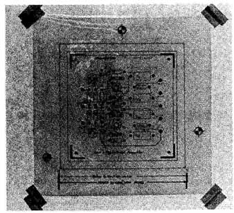
FIG. 7 Completed pad master with the underlying component lay out drawing
for the preamplifier circuit.
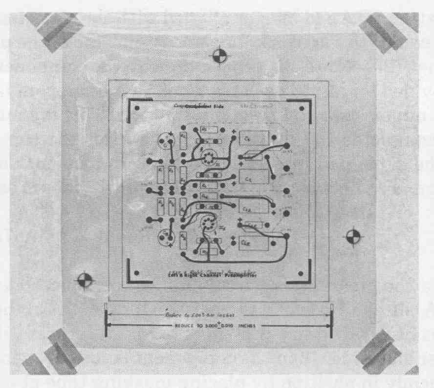
FIG. 8 Completed component-side taping with underlying pad master for
the preamplifier circuit.
5. COMPONENT-SIDE ARTWORK MASTER FOR THE PREAMPLIFIER CIRCUIT
To produce the artwork master for the component side of the preamplifier circuit, another sheet of acetate is placed directly over the pad master just completed. This sheet should be slightly larger than the pad master so that the masking tape used to secure it in place will not interfere with the tape holding the pad master. This will enable the component-side layout to be removed with out upsetting the registration between the underlying pad master and the component layout drawing. On this component-side acetate sheet, all conductor path routing to complete this side is laid out. (Reference should be made to Sec. 11.6 for techniques for taping conductor paths.) Only those conductor-path traces drawn in red pencil on the component layout drawing will be taped. The tape should overlap the solid donuts and not butt them. No line drawn with blue pencil should be taped onto this artwork master. Upon completion, the taping of each path should be checked for accuracy in tape routing and for optimum path positioning to obtain the widest space between the path and any adjacent copper features along its route.
The component-side layout is a view of the pc board as it appears when viewed directly. Therefore, all literal and numerical information should appear right-reading on this acetate sheet. The finished layout of the component side of the amplifier pc board, together with the underlying pad master, is shown in FIG. 8. Component keying and labeling may be included on this side since their application to the acetate is simpler due to the fact that they appear right- reading. Before the component-side layout is removed from the pad master, three grid locators should be accurately positioned directly over those on the pad master. These will later be used for registration and alignment after the artworks have been removed from the drafting board and are to be photo graphed.
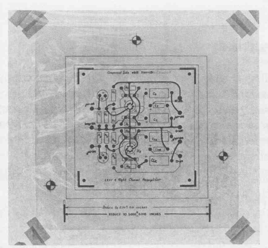
FIG. 9 Completed circuit-side taping with underlying pad master for
the preamplifier circuit.
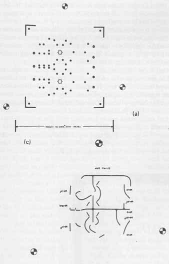
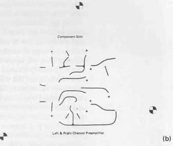
FIG. 10 Individual elements of the preamplifier circuit using a three-acetate
system: (a) pad master; (b) component side; (c) circuit side.
6. CIRCUIT-SIDE ARTWORK MASTER FOR THE PREAMPLIFIER CIRCUIT
After the component-side layout has been completed, it is removed and temporarily set aside being careful not to disturb the underlying pad master. Another sheet of acetate is positioned over the pad master to construct the circuit-side layout. This is done with the same procedure used for construction of the component-side layout except only those traces drawn in blue pencil on the component layout drawing are to be taped. When completed and checked, lettering is applied in a reverse-reading orientation, as is done for single-sided board layouts. Reverse-reading dry transfers are available or the acetate sheet may be removed from the pad master and right-reading lettering applied to the back of the sheet. The circuit-side layout for the preamplifier pc board, together with the underlying pad master, is shown in FIG. 9. The pad master with the component-side layout and the circuit-side layout are shown in FIG. 10.
7. LAYOUT CONSIDERATIONS FOR PLATING
Section 19 describes the process of pattern-plating both copper and 60/40 tin- lead alloy onto the conductor path areas of both sides of the pc board. Many of the problems associated with an improper balance of plated metals can be attributed to the component layout drawing and the taped artwork masters. If a double-sided pc board is to be electroplated to a uniform thickness and proper alloy, it must meet the following specifications:
1. The total conductor pattern areas to be plated on each side of the board must be as close to equal as possible.
2. The conductor pattern on a given side of the board must be uniformly and evenly distributed throughout.
Strict adherence to the specifications above is essential if the correct 60/40 tin- lead alloy is to be deposited during the plating process. An imbalance of conductor pattern areas between the two sides results in the side with the less area to be tin-rich-plated and the side with more area to be lead-rich-plated. If the ratio of alloys plated on either side is significantly different from the optimum 60/40 ratio, proper soldering of the board will not be realized.
If the conductor pattern is not uniformly and evenly distributed across either side of the board, the area with the heavy concentration of copper conductors will be low in tin-content plating, while the area with the light concentration of copper conductors will be plated with an alloy having high tin content. This will again result in soldering difficulties.
One final provision that must be included in the conductor pattern layout
phase for boards that will be electroplated is an area of solid copper
just outside the corner brackets of the pc board. This area is called
the thief or robber area and its purpose is to direct some of the high
current density at the edge of the board toward itself during the plating
process. This will result in a more consistent 60/40 alloy on both sides
of the pc board. The thief area is added to the preamplifier pad master
just outside the corner brackets with the use of appropriate-size tape.
The processed negative should have a thief area between and 1 in
ch wide
after reduction. The inclusion of this taped thief area on the pad master
results in its appearance on both sides of the board. The pad master
for the preamplifier circuit with taped thief area is shown in FIG. 11.
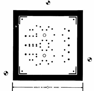
FIG. 11 Completed pad master with taped thief area.
8. DIAZO PHOTOTOOL FOR DOUBLE-SIDED PRINTED CIRCUIT BOARDS
For photographic reduction, the component-side layout is placed over the pad master on the camera copyboard and photographed. It is then removed from the copyboard and the circuit-side layout is placed over the pad master and another exposure is taken. Perfect registration is maintained with this system since the pad master is the same for both sides of the pc board.
The taped artwork masters are photographically reduced into two 1 : 1 scale negatives as described in Section 12. For processing a double-sided pc board with plated-through holes, two 1 1 scale positives are required. These silver halide positives are generated from contact-printing the negatives. (Con tact printing is discussed in Section 12.) Silver halide positives, however, are not suitable for proper registration as will be explained here. Correct registration of the 1 : 1 phototools on both sides of a previously drilled panel is accomplished by aligning the solid terminal pads of the phototools over the holes. The aim is to obtain uniform annular rings about all holes. Because the conductor pattern on silver halide positives is 100% opaque, the drilled holes cannot be viewed through the pads on the positive to obtain proper registration. For this reason, phototools must be made from the 1: 1 silver halide positives which have a lower visual density (light-transparent color) of the opaque conductor pattern yet be opaque to ultraviolet radiation. These positives will allow the drilled holes to be viewed through the pads for proper registration.
One type of film available for producing this special phototool is a light- sensitive diazo emulsion film on a polyester base. Diazo film, whose emulsion is sensitive to ammonia gas and is commonly used in the pc board industry, makes direct image transfer (without reversal) when contact printed with standard silver halide positives. The contact printing is accomplished under gold safe-light conditions using the same ultraviolet light-exposure units used for photo-resist exposure (see Section 18). The film is then dry-developed in hot ammonia gas.
To illustrate the process of producing two diazo phototools (one for the component side and one for the circuit side of the preamplifier circuit), we will use Dynachem Type G-2 Trans Opaque film. This diazo film is supplied on a dimensionally stable 0.007-inch polyester base. It should be stored at 50°F (10°C) or below when not in use in order to extend its shelf life. It is always processed in a gold safe-light environment such as that found in the photo-resist exposure area of a pc board fabrication facility.
To make a 1 : 1 contact-printed diazo positive from a silver halide positive, a sheet of G-2 film is first placed in the vacuum frame of an exposure unit (similar to the one shown in Fig. 13.3a) on a black nonreflective surface. The film is positioned with the emulsion side facing upward. In this position, the notch on the sheet of film will be in the upper right corner. The silver halide positive is then placed on top of the diazo film with its emulsion side down. The frame cover is closed and the vacuum pump is turned on which will bring both films in tight contact with each other before sliding the frame under the expo sure lamps. Exposure time is determined empirically. It has been found that with the 400-watt ultraviolet light source shown in Fig. 18.10, proper exposure is completed in under 2 minutes. Those areas on the diazo film which are exposed to the light through the transparent areas of the silver halide positive will remain clear when developed in ammonia gas. Those areas under the opaque conductor pattern of the silver halide positive are unexposed to the light. In the diazo developing process, these areas became an amber color which is transparent to visible light but opaque to ultraviolet light.
After the diazo film has been exposed, it is removed from the vacuum frame and developed in a gold-lighted area using a Dynachem Diazo G-2 Film Processor, which is shown in FIG. 12. This unit is a simple conveyor having hard-rubber rollers which transport the film slowly through an environment ammonia gas heated to 200 to 220°F (93 to 104°C). By simply introducing the film into the unit, total developing time is approximately 1 minute.
When the diazo film has been developed, the amber conductor pattern image will become visible (see FIG. 13). Since it is now possible to s through the solid terminal pads, proper registration of the film over a predrill board can be effectively accomplished.
Since the processed films will be used as phototools to image pc board they must have areas that will effectively block ultraviolet light and other areas that will transmit UV energy. This is true for both silver film and diazo film. With diazo film, the amber areas must block UV light while the clear portions transmit UV energy. Accurate measurements of the ability of the film areas to block or transmit UV light can be obtained easily arid quickly with the use of a Macbeth Transmission Densitometer. This is shown in FIG. 14. To use the instrument, the two areas of film are alternately placed over the sampling area and readings are shown on a digital display. The opaque area that is to block UV light must show a reading of 4.00 or greater. The clear portion must produce a reading of 0.6 to 0.7 for diazo film and 0.02 to 0.06 for silver films to ensure effective transmission of UV energy.
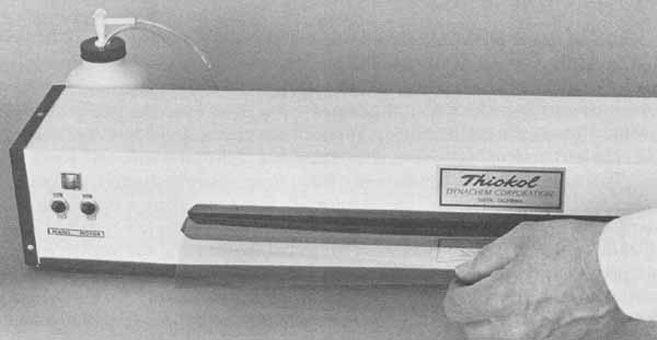
FIG. 12 Exposed film being developed with the Dynachem diazo developing
unit.
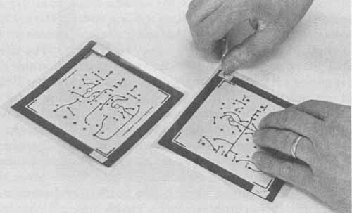
Fig. 13 Diazo film phototools with double-sided masking tape.
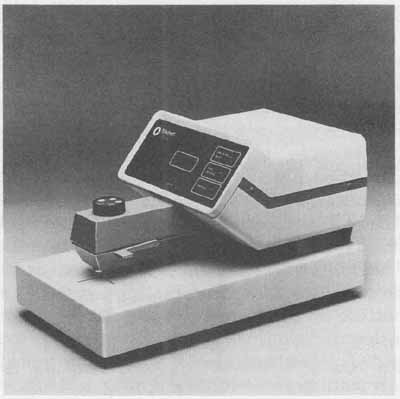
FIG. 14 The densitometer measures the UV filtering and transmission
characteristics of phototools. Courtesy of Macbeth, a division of Kollmorgen
Corporation.
The procedure for using the densitometer is as follows:
Step 1. The filter wheel is rotated to the UV position. This places the ultraviolet filter at the sampling aperture.
Step 2. The rocker switch located on the rear panel is turned on. Three figure Cs will appear on the digital display and the light in the density button will appear.
Step 3. The sampling aperture arm and the zero button are pressed simultaneously, resulting in 0.00 to appear on the display.
Step 4. The calibration film strip is placed under the sampling aperture and depressed. This should result in a reading of 3.00. If a different reading is displayed, the CAL TRANS potentiometer on the rear panel is adjusted for a reading of 3.00.
Step 5. The sampling aperture arm is released and the calibration film removed.
Step 6. The diazo films amber area (black for silver halide) is placed under the sampling aperture and depressed. A reading of 4.00 or greater should be displayed to indicate a properly exposed and developed film.
Step 7. The sampling aperture arm is released and the film is shifted to a clear area and the aperture again depressed. For effective UV transmission, readings of 0.02 to 0.06 should be displayed for silver film and 0.6 to 0.7 for diazo film.
The densitometer is an important instrument in assuring the effectiveness of the phototools to filter and transmit UV energy.
Final preparation of the phototools requires that the two sheets of diazo film first be cut to size. Two pieces of double-sided Scotch or masking tape are then placed on each phototool on the side which will contact the photosensitized pc board during exposure ( Section 18). This is the side where the literal information appears reverse-reading. The tape ensures that registration will be maintained between the phototool and the pc board throughout the exposure process.
With the completion of the diazo phototools, we will continue with the discussion of the sequential processes in the fabrication of a double-sided plated- through-hole pc board. Because these processes are very involved and require a great deal of detailed explanation, they will be spread over the next three sections. Section 17 will present the drilling of the bulk stock and its preparation for copper deposition followed by a flash-plating process. Section 18 discusses the conductor pattern imaging process using dry film photo-resist and the diazo phototools described in this section. Section 19 completes the fabrication of a double-sided plated-through-hole pc board by considering copper pat tern plating, solder plating, photo-resist stripping, etching, and infrared solder reflow.
AMAZON multi-meters discounts AMAZON oscilloscope discounts
EXERCISES
A. Questions
1 Describe specifically how interconnections are made between the circuit side and the component side of a double-sided plated-through-hole board.
2 What is the recommended grid system and reduction scale for double-sided pc board layouts?
3 What is the color-coding scheme for double-sided component and conductor pattern layouts?
4 When placing literal and numerical information on double-sided lay outs, what is the convention in regard to right- and reverse-reading directions?
5 List the main advantage of each of the taped artwork systems de scribed in Sec. 3.
6 Describe the main elements of the donut master taped artwork system, being specific as to what should appear on each element.
7 To achieve uniform plating, what two layout specifications must be adhered to in circuit board design?
8 What is the purpose of the thief area?
9 What might be a possible cause of tin-rich plating?
10 Why is diazo film chosen over silver halide film for phototools used to image double-sided pc boards?
B. True or False
Circle T if the statement is true, or F if any part of the statement is false.
1 The bottom side of a double-sided pc board is also referred to as the circuit side. T F
2 A PTH forms a continuous metal path between copper on the top and bottom sides of a double-sided pc board. T F
3 Bodies of components, such as resistors and integrated circuits, must not contact conductor paths on a pc board. T F
4 On a composite view of both sides of a double-sided pc board, conductor paths must not be allowed to cross each other. T F
5 Annular ring is the term used to describe the amount of copper remaining after a copper pad is drilled. T F
6 The two-acetate system for preparing taped artwork masters is used to achieve perfect top-to-bottom side registration. T F
7 The purpose of the thief area is to direct some of the high-current density at the edge of the board toward itself during the plating process. T F
8 Ultraviolet light will not pass through black areas of silver halide film but will pass through the amber-colored areas of diazo film. T F
Multiple Choice
Circle the correct answer for each statement.
1 All literal and numerical information should be (right-, reverse-) reading on the component side and (right-, reverse-) reading on the circuit side of a double-sided pc board.
2 The preferred method of preparing double-sided pc board artwork masters is the (one-, two-, three-) acetate method.
3 The misalignment of donut pairs is eliminated when using the (one-, two-, three-) acetate method of artwork generation.
4 (Diazo, silver halide) film uses an emulsion that is developed in a dry ammonia gas.
5 Diazo film is exposed using (ultraviolet, infrared) source of light.
D. Matching Columns
Match each item in column A to the most appropriate item in column B.
COLUMN A | COLUMN B
1. Diazo 2. Thief area 3. PTH 4. Annular ring 5. Three-acetate system 6. Circuit side |
a. Plated-through hole b. Donut master c. Bottom d. Ammonia gas e. Breakout f. Plating |