AMAZON multi-meters discounts AMAZON oscilloscope discounts
LEARNING OBJECTIVES:
.Upon completion of this section on the description and the packaging of a high-fidelity stereo amplifier system, the student should be able to:
1. Understand the function of each subassembly of the amplifier system.
2. Understand the interrelations of each of the subassemblies in the amplifier system.
3. Differentiate between chassis ground and single-point ground.
4. Understand the selection criteria for each of the components used in the amplifier system.
5. Provide heat sinks for devices dissipating high power.
6. Sketch the approximate placement of the major components in the amplifier system.
7. Develop a preliminary sketch of the chassis and enclosure elements for the amplifier system.
0. INTRODUCTION
A stereo amplifier, employing many of the latest semiconductor devices, is used as a means of illustrating the practical applications of packaging techniques discussed in this guide. In this way, familiarity is gained with the application of the latest design considerations, conventions, and practical procedures for sound electronic packaging.
Since a basic understanding of the electronic circuitry involved is essential in order to fully interpret and apply the necessary procedures for packaging, a brief discussion of the circuit’s electronic operation and special characteristics is presented here.
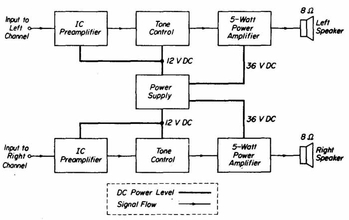
FIG. 1 Block diagram of the stereo amplifier. Subassemblies and their
interrelationships are shown by signal flow paths and dc power levels.
The block diagram of the amplifier is shown in FIG. This type of diagram identifies the function and interrelationship of each circuit. FIG. 2 shows a detailed schematic diagram of one channel of the amplifier and the power supply. Only the left channel is shown because the right channel is an exact duplicate.
Incoming audio signals from an AM (amplitude modulation) tuner, FM (frequency modulation) tuner, or magnetic phonograph cartridge must be in creased in power from their relatively low output levels (millivolt range) to a level sufficient to drive a low-impedance speaker, such as the 8-ohm speaker shown in FIG. Not only must the incoming signal be increased in level, but the output must also be a faithful reproduction of the input. For this reason, relatively sophisticated circuitry is necessary. Although FIG. 1 appears to be complex, this entire diagram represents a complete system composed of seven individual but related circuits. Therefore, to most readily grasp a basic under standing of the operation of the system, the function of each circuit must be investigated. This will serve as an essential guide to the technician for isolating all the important packaging problems. Notice that this system consists of two channels. Each channel is terminated with its own speaker and all circuits in each channel are energized from one common power supply.
The first circuit that the signal encounters in either channel is the preamplifier. The purpose of this circuit is to amplify a signal level of only a few milli volts to a voltage level on the order of 500 millivolts. This increased level or amplified signal is now large enough to drive the power amplifier once it passes through the tone control circuit. The preamplifier consists of a single active device or integrated circuit (IC) with its support components (resistors and capacitors) through which the first increase of input signal magnitude is achieved.
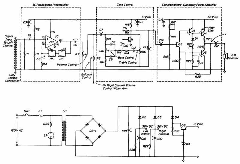
FIG. 2 Schematic diagram of one channel of the stereo amplifier and
power supply.
The increased signal of each preamplifier output is next applied to the in puts of the tone control circuit. The function of each tone control or frequency shaping network is to allow the operator to select and compensate for individual listening preferences in program material. The human ear tends to detect higher frequencies, at the same output level, more readily than lower frequencies. Consequently, the operator may find it desirable to increase or decrease the low-frequency output level without altering the high-frequency level. This technique, called base boost or low-frequency cut, respectively, is possible with the tone control. Treble control capability is also provided with the tone control circuit by boosting or cutting high frequencies. Each channel’s tone control circuit consists of a high-frequency, high-gain silicon transistor with the associated frequency-selective circuitry performing the tone shaping from the transistor’s input to output. Control is achieved through two potentiometers, with the bas treble control independently adjusted. These tone control potentiometers can also be adjusted for flat control (neither cut nor boost) wherein the gain is unity for all frequencies. In this mode of operation, the out put level of the tone control is equal to the output level of the preamplifier and is sufficient to drive the power amplifiers to their full output. The complimentary-symmetry power amplifiers represent the final stage of signal amplification. The function of the power amplifiers is to provide the necessary voltage and current to drive the speakers while maintaining the proper impedance match for maximum power transfer to these speakers.
Although both channels of the amplifier are operated independently of each other to reproduce stereophonic program material, they receive power from a common supply. This power supply must provide two levels of dc out put. The lower level, 12 volts, is used to energize the preamplifiers and tone control circuits. The higher voltage level, 36 volts, is used to operate the power amplifiers.
The schematic diagram of FIG. 2 will now be discussed in detail, not only to increase the technician’s familiarization with each individual circuit, but also as an aid to understanding specific packaging problems related to these circuits. The operation of the power supply and one channel only will be described since, as mentioned previously, the second channel is an exact duplicate. How ever, both channels will be constructed throughout the text to form a complete stereo system. Since this system is designed to faithfully reproduce audio frequencies (20 hertz to 20 kilohertz), higher-frequency packaging problems are not considered.
1. PREAMPLIFIER
The preamplifier circuit shown in FIG. 2 utilizes a 741 high-gain, wideband integrated circuit operational amplifier (op-amp) with a relatively high input impedance. The input signal is restricted to a maximum value of 10 millivolts (rms). If this signal level is exceeded, the power amplifier will be overdriven, thus distorting the signal and reducing the bandwidth of frequencies to be faithfully reproduced and amplified. The input signal is applied to the non- inverting input terminal of the op-amp through a phono jack. The use of this type of jack is essential so that shielded wire can be used between the input source and the preamplifier. All precautions should be taken to eliminate undesirable pickup or noise from the input of the preamplifier because this noise will be amplified along with the signal. Shielded cable protects against pickup by shorting undesired signals to ground. Resistors R1 and R2 provide the proper input bias current for the op-amp inputs. The input impedance for the preamplifier circuit is R1, R2 and R3 in parallel, or approximately 47 kilohms, which is suitable for magnetic cartridge impedance matching. Since magnetic cartridges are nonlinear in their response, one function of the preamplifier is to compensate for this characteristic. This is accomplished by the equalization circuit R6, R6, C4 and C5 Voltage gain is controlled by the ac feedback network, consisting of the equalizing circuit together with R and C Resistors R and R also supply dc feedback to the inverting terminals of the op-amp to stabilize the operating point.
Because aluminum is an excellent electrical conductor, common, or ground, points are often connected to the chassis. This technique is called chassis ground. A problem may arise in the use of chassis ground that should be pointed out. If the terminal points are connected to many widely separated locations on the chassis, the small amount of resistance in the aluminum may be just enough to set up a potential difference among these points. This condition is known as a ground loop. The path of this loop may include the input of the amplifier and would therefore introduce an undesirable signal between output and input. To prevent the possibility of ground loop in this amplifier system, the circuit should be connected to the chassis at only one point. Usually, a point as close as possible to the amplifier input jacks is chosen for this purpose.
The output of the preamplifier, through coupling capacitor C6 is coupled to volume control R7, which adjusts the signal to the tone control input. R8 is the balance control. Each side of this potentiometer is connected to the wiper terminals of the volume controls. The wiper of the balance control is connected to the common side of this circuit. (Of course, balance control is eliminated if only one channel is to be used.) R8, then, controls the relative signal level from each channel being delivered to the tone control circuit.
2. TONE CONTROL
Coupling to the tone control is provided through C7. Transistor Q1 is biased at its low noise point by R15 and the adjustable local feedback resistor R Base boost and base cut control is accomplished by R9, R10, R11, C8 and C9. With the wiper of R10 in the uppermost position (boost), represented by a clockwise rotation of the control shaft of the potentiometer, the gain of the amplifier at low frequencies is the ratio of R9 to R10 As the frequency increases, capacitor C9 bypasses R10 and at approximately 600 hertz the gain of the amplifier approaches unity. The treble control consists of C12 and R16 High-frequency gain is approximately equal to the ratio of the bottom part of R16 to the top part of R16 as determined by the wiper section. The tone control circuit is decoupled through C11 Wiring of this circuit is critical in terms of reducing pickup of undesired signals. Consequently, all lead lengths should be as short as possible.
3. POWER AMPLIFIER
The output of the tone control is coupled to the complementary-symmetry power amplifier through C14. The input impedance to this amplifier is approximately 20 kilohms. The circuit requires 0.5 volt rms to deliver a true power out put of 5 watts. Resistors R17, R18 and R19 provide bias to the transistor Q12, R17 should be adjusted to establish point x (the common point of R23, R24, R25 and C17 at a potential of approximately 18 volts (0.5 Vcc) with no signal applied. Transistor Q3 is the driver for the complementary output transistors Q4 and Q5 The driver must be able to dissipate approximately 1 watt and will require heat sinking for safe operation. Resistor R25 provides both dc and ac negative feed back, to allow for operating point stability and gain stability. Operating-point temperature compensation can be achieved by mounting diode D1 on the common heat sink provided for Q4 and Q5 so that it encounters the same thermal conditions as these transistors. R21 can be adjusted to minimize crossover distortion. Capacitor C17 isolates the speaker from the dc current of the power supply.
Since Q4 and Q5 must dissipate 25% of the rated output power under maximum load conditions, they will require heat sinking. An aluminum plate 3/16-inch thick by 2 inches by 3 inches should be used as the minimum-size heat sink. Because the circuit for this power amplifier makes no provision for short-circuit protection at the output, care must be exercised to prevent the output terminals from being shorted when the speakers are connected.
4. POWER SUPPLY
The dc power to the stereo amplifier system is supplied by transformer (T1) conventional bridge rectifier DB1, and filter capacitor C18. Diodes D2 and D3 are used for channel separation. Capacitors C19 and C20 provide additional filtering for the 36 volts for the power amplifiers, which is obtained at the cathodes of the diodes D2 and D3. The 12 volts necessary to power the preamplifier and tone control circuits is obtained through the use of an emitter follower regulator that establishes its reference 12 volts from zener diode D5. No diodes are necessary for separation when a regulator is used. Therefore, both channels may be driven from the emitter of Q6, D4 is used to separate the regulator from both channels.
5. AMPLIFIER PACKAGE DESIGN
Normally, a semiconductor amplifier has little space or weight restrictions. Therefore, the first phase in the design of this amplifier package will be the selection of components and hardware. Resistors and capacitors are selected on the basis of the circuit’s voltage, current, and power requirements. The power levels in circuits of this type are generally very low. For this reason, as well as for their small physical size, 1/2-watt resistors will be used throughout the design with the exception of R22, which must be capable of dissipating at least 2 watts, and R23 and R24 which must dissipate at least 1 watt. All these resistors will have a tolerance of 10%. Electrolytics will be used for coupling and decoupling capacitors as well as in the power supply filter circuit, owing to the larger capacitive values required for these applications. Electrolytic capacitors are selected over other available types because they provide the large values of capacitance required with the smallest physical size. The balance of the capacitors in the system will be the disc type. These have the advantage of possessing an extremely high leakage resistance. In addition, their small physical size makes them easily adaptable to printed circuit design. The working voltage for the disc capacitors, based on circuit requirements, will be 100 volts and for the electrolytics, 50 volts.
The power transformer (T1) selected is rated at 25.2 volts at 2.8 amperes, even though the circuit is not expected to draw more than 1.6 amperes. Diodes, transistors, and integrated circuits are selected in the same manner, with the voltage, current, and power requirements of the circuit being satisfied. Cost and availability serve as secondary factors in determining the choice of these components.
Initially, a parts list will be prepared. This list must be complete, including not only the components but also the associated hardware and materials to complete the package. FIG. 3 shows the complete list of components and parts for the amplifier. As much information as possible should appear on the parts list, such as types, ratings, and tolerances.
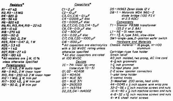
FIG. 3 Parts list for stereo amplifier.
The type of aluminum that will be used for the chassis, front panel, and enclosure elements will be 16 gauge, No. H-1100. This choice is made on the basis of the desirable characteristics of this material—easily worked, sturdy, lightweight, conductive, and readily available. The heaviest component (trans former T weighs less than 32 ounces and is easily supported by this material. In addition, aluminum lends itself readily to the finishing techniques discussed in Section 9.
The box-type chassis, shown in FIG. 5b, will be selected for this design. Even though the heaviest component in the system weighs less than 2 pounds, the box chassis possesses advantages other than strength. It is most suitable for mounting printed circuit boards (which must be used in this type of circuitry), wherein large areas of metal can be removed from the top surface with out seriously weakening the overall chassis.
A preliminary sketch of the amplifier component layout is next under taken. This sketch is made simultaneously with the technique of positioning the components on a similar mounting surface to that selected for the final package. A preliminary sketch of the amplifier chassis is shown in FIG. 4. This type of pictorial is necessary to fully appreciate whether or not the chassis style and shape are completely compatible with both the functional and esthetic aspects of the design.
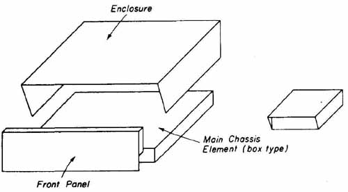
FIG. 4 Preliminary sketch of intended style for the chassis, front
panel, and enclosure elements.
A starting point in the packaging layout is the placement of the power transformer which should be mounted as far as possible from the amplifier’s inputs to avoid the possibility of introducing 60-hertz hum. For this design, the transformer (T1) will be mounted on the top right-hand rear corner of the chassis. This will allow the power cord to enter directly into the rear of the chassis. Some form of restraint or clamp is necessary to secure the line cord. This pre vents undue strain on terminals or the wires from separating from soldered connections if the cord is roughly handled. The pilot lamp will be mounted on the front panel for ease of observation. This location, however, will require a twisted pair of leads between the lamp base and the primary winding of the transformer. This twisting of the leads cancels the generated magnetic field about the leads, thereby preventing hum. The power supply circuit will be positioned close to T to further minimize lead length carrying 60-hertz frequency. Power for the preamplifier, tone control, and power amplifier circuits should be provided on the side of the power supply printed circuit board closest to these circuits.
Since the circuit is fused on the primary side of the transformer, the fuse holder will be a cartridge or extractor post type, which is mounted through the rear of the chassis close to the power cord. This type of fuse holder is extremely safe with respect to fuse changing, since its design eliminates the possibility of electrical shock.
All control knobs will be mounted on the front panel and generously spaced for balanced appearance and ease of operation. The position of the potentiometers will influence the placement of the tone control circuit in terms of short lead length. All input and speaker connections will be to the rear of the chassis to keep their leads from interfering with the operation of the controls and to preserve the appearance of the package. Phono jacks will be used for input connections to the unit to take advantage of the shielding of the input leads associated with this type of connector. Insulated screw-type jacks will be used for the speaker connections, although phone jacks also could be used.
The various types of mounting hardware, such as machine screws, nuts, washers, sheet metal screws, and special fasteners, are discussed in Section 23. The terminals on the printed circuit boards used for interconnecting wiring will be the wire-wrap type. This terminal is readily adaptable to printed circuit work because of its small size. In addition, it is more economical when plug-in modular design is not required, as is the case with this stereo system. (Printed circuit hardware is discussed in Section 14.)
Because of the number of components involved and overall circuit complexities, each of the seven circuits in the system will be packaged on an individual pc board. This technique has several advantages over other packaging arrangements, the most important being that each individual circuit in the system can be designed, constructed, and individually tested. Upon completion of these individual circuits (i.e., the power supply, preamplifiers, tone controls, and power amplifiers) simple interconnections among these pc boards will re suit in a functional amplifier system.
Along with all the inputs, the preamplifiers (the first stage of signal input) will also be positioned to the rear of the chassis. The numerous connections and terminals on the tone control dictate that these pc boards be positioned for ward so that they can be connected conveniently to the panel-mounted potentiometers. The output terminals of the power amplifiers will be positioned to the rear of the chassis to minimize lead length to the speaker terminals. Finally, the power supply pc board will be placed as near the transformer as possible. FIG. 5 shows a layout of the chassis with the intended individual board locations in addition to some hardware and component placement. This layout helps in estimating if wiring will be interconnected simply and conveniently.
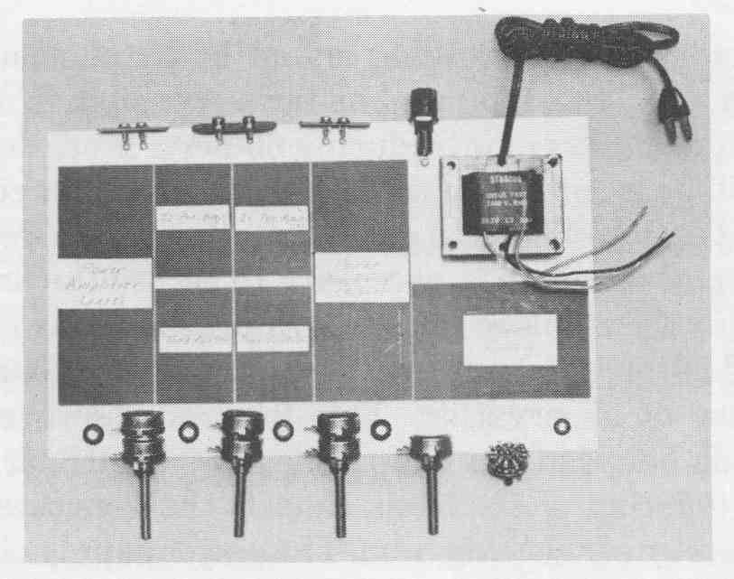
FIG. 5 Chassis layout with intended PC board locations and major hardware
and components positioned.
At this stage, it is not important to consider the exact component positioning on the pc boards. All that is necessary is to determine the approximate component layout to gauge the correct overall size of these boards and their exact location with respect to the associated chassis-mounted hardware and components whose position is dictated by external connections. For example, input and output coupling capacitors must be mounted to an edge of a board closest to their chassis-mounted terminals. The interconnections among boards will also determine the relative positions of these components ( FIG. 6). To maintain a balanced appearance, the control shafts of the base, treble, volume, balance, and on-off controls will be spaced evenly across the front panel.
A sketch of the final placement of the components is completed when the desired location of all parts has been determined and a reasonable balance has been achieved. FIG. 7 shows the results of major component positioning and mounting-space requirements. From this layout, the optimum-size chassis, panel, and enclosure elements can be designed and fabricated.
To convert the final layout into useful detailed drawings for the actual construction of the unit, accurate measurements of components and their locations must be made. Procedures for determining accurate dimensional information and the application of this information in the preparation of detailed drawings are discussed in Section 3.
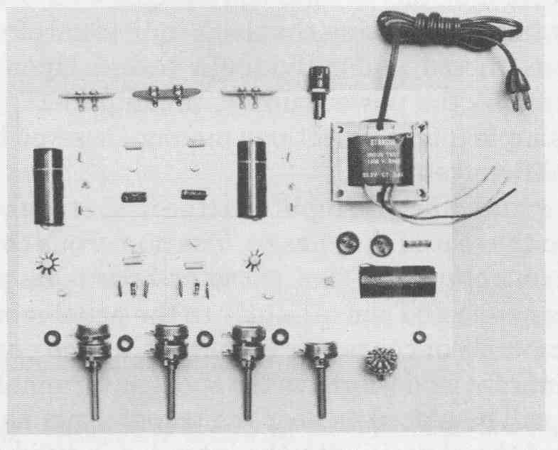
FIG. 6 Major PC board components are positioned to observe if any interconnecting
problems will be encountered.
EXERCISES
A. Questions
1 What are the significant differences between block diagrams, schematic diagrams, and component layouts?
2 For determining chassis size, what components are normally located at the perimeter of the chassis layout?
3 Explain the term balanced layout as it applies to electronic packaging.
4 What is the difference between chassis ground and single-point ground?
5 List the three major subassemblies of one channel of the stereo amplifier that are connected to the power supply subassembly.
6 Give one example of the application of human engineering in the layout of the stereo system.
7 Which chassis configuration is best suited for the packaging of the stereo system?
B. True or False
Circle T if the statement is true, or F if any part of the statement is false.
1 The position of individual components can readily be determined from a block diagram. T F
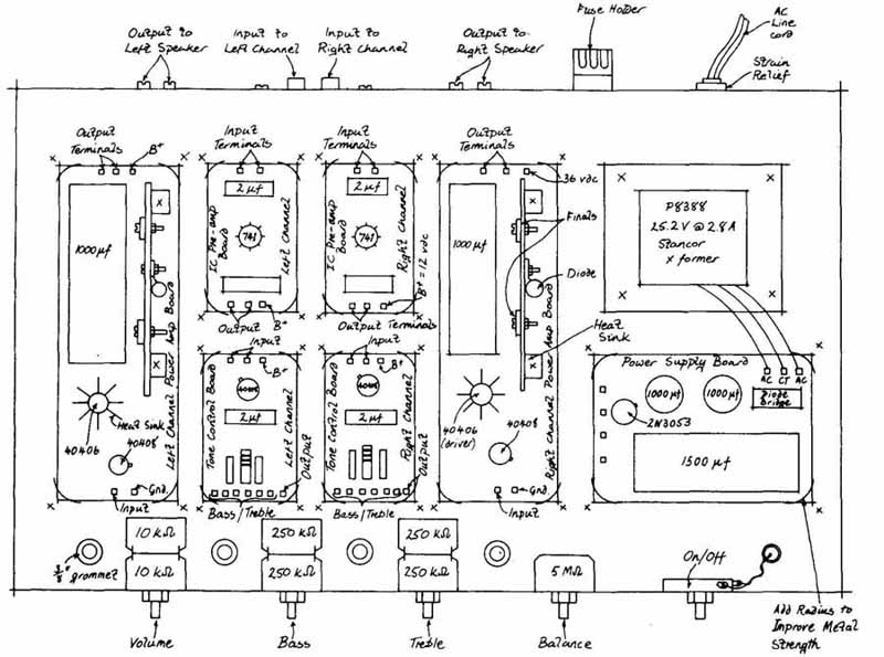
FIG. 7 Sketch of major component positioning for the stereo system.
2 Schematic diagrams show the continuity of wiring connections between all the components. T F
3 The purpose of a preamplifier is to amplify a small signal level to a voltage level several hundred times larger. T F
4 The signal level passing through the tone control circuit will be slightly higher at its output. T F
5 The tone control circuit can be a source of undesired signal pickup if not wired correctly. T F
6 The size and style of all components can be determined from the parts list. T F
7 A balanced layout in an electronic system deals more with uniformity of spacing without crowding than it does with symmetry. T F
C. Multiple Choice
Circle the correct answer for each statement.
1 The exact electrical connections for each component in an electric circuit is best shown by a (block, schematic) diagram.
2 The preamplifier of our stereo system is used to increase the input signal from a few (microvolts, millivolts) to approximately 0.5 volt.
3 Low-frequency signals can be increased by base (boost, cut) in the (tone control power amplifier) section of our stereo system
4 Capacitor C in FIG. 2 blocks (dc, ac) current from entering the speaker.
5 (Disc, electrolytic) capacitors are used when large capacitance values are required.
6 To prevent the possibility of ground loops, a stereo system should be connected to its metal chassis at (one, many) points.
7 Aluminum is selected for the chassis elements of our stereo system because it is a good (conductor, insulator) of electricity.
8 Good design dictates that all control knobs in a stereo system be positioned at the (front, rear) of the package.
9 The main chassis element for our stereo system is a simple (box, U-shaped) type.
D. Matching Columns
Match each item in column A to the most appropriate item in column B.
COLUMN A COLUMN B
1. Fuse 2. Working voltage 3. Tone control 4. Transistor 5. H-1100 6. Ground 7. Hum 8. Box type |
a. Q b. Loop c. 60 hertz d. Cartridge e. Chassis f. Capacitor g. High-frequency cut h. Aluminum |
E. Problems
1 Determine the approximate parts position and chassis element configurations for packaging just the power supply section shown in FIG. 2
2 Give the complete package design for just the two-channel preamplifier and tone control combination taken from FIG. 2 using four separate printed circuit boards.
3 Show the complete package design for the two-channel preamplifier and tone control circuits using only two separate printed circuit boards.
4 Show the complete package design for just the power amplifier and power supply sections of FIG. 2
5 Estimate the maximum amount of 16-gauge aluminum or 18-gauge steel required to fabricate all the chassis elements selected for Problems 1, 2, 3, and .4 from blank stock.
6 Using industrial electronic component catalogs determine the cost per watt of just the power amplifier and power supply sections of the stereo system shown in FIG. 2