Salvaging Fluorescent Displays
A.G. Blewett, Ramsey
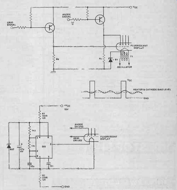
Multi-digit vacuum fluorescent displays (multiplexed operation) are widely available from 'junked' calculators and surplus sources. Unfortunately they are not as easy to use as LED displays, because they need an AC filament supply to ensure even brightness, and this supply needs to be DC biased, because the display operates just like a valve (remember them?). Figure 2 summarizes the drive requirements.
In many calculators, this is achieved as in Fig. 1. A transistor oscillator feeds the isolation transformer T1, which supplies current for the filament. The center-tapped secondary allows the filament (cathode) to be referenced to ground via a zener, so as far as the cathode is concerned the grids and anodes are negative when grounded through R,A and R, . Taking these high via the transistors positively biases them, enabling the display.
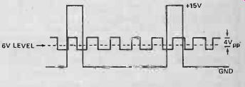
Providing you don't need to conserve battery power, the circuit of Fig. 3 provides a convenient alternative to messing about with oscillators and ferrite transformers, and allows single rail operation.
The 555 timer is connected in the astable mode, and supplied from the 4V7 zener. It drives the display filament direct, because the relationship of R1 and R2 gives the correct bias levels to the display electrodes.
The resulting,-waveforms are summarized in Fig.4.The 555 produces about 4 V peak-to-peak on load, which is 2 V,, just about right for correct filament operation.
Display brightness can be increased by increasing V«, but if this is done, the values and wattages of R1 and R2 will have to be changed as well.
Cheap Voltage Reference
A. Parker, Leicester
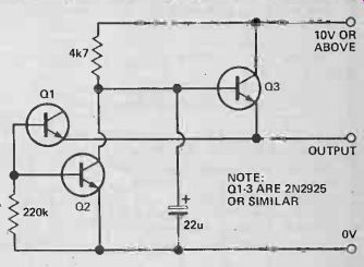
This circuit forms a cheap voltage reference, with the reverse base-emitter breakdown voltage of Q1 in series with the forward base-emitter voltage of Q2 providing the reference element. With this configuration the temperature coefficients of the two base-emitter junctions almost cancel one another out and although separate transistors are shown for cheapness, a dual transistor such as the LM394 could be used to advantage.
C1 is used to decouple the noise generated by the zener action of Q1 while Q2 is an emitter follower which, with the values shown, gives at least 20 mA. The reverse base-emitter breakdown voltage of silicon transistors usually lies around 5 V for RF types and up to approximately 9V for audio types.
-------------
Tech-Tips is an ideas forum and is not aimed at the beginner. We regret we cannot answer queries on these items. ETI is prepared to consider circuits or ideas submitted by readers for this page. All items used will be paid for. Drawings should be as dear as possible and the text should preferably be typed. Circuits must not be subject to copyright. Items for consideration should be sent to ETI TECH-TIPS, Electronics Today International, 145 Charing Cross Road, London WC2H OLE.
---------
Variable Stereo Field
F. Vanthuyne, Belgium
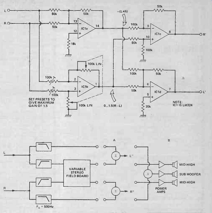
Here is a simple circuit, using only one IC, with which the usual stereo field can be varied from mono, over normal stereo, to 'super stereo'. The effect is controllable by only one (stereo) potentiometer: for the left channel from L' = (L + R)/2 (mono) to L' = 2L -R (superstereo), and for the right channel from R'=(R+ L)/2 to R'= 2R -L. Unity gain is preserved through the entire control range. Pin numbers are given for the 324 quad op-amp, but this IC may be replaced by a lower noise type if desired.
Resistors must have 1% tolerance because, if not, sounds in the center of the normal stereo field may be attenuated in the superstereo position. The effect has to be connected between the preamp and power amp of a stereo system or, in the simplest case, one can use the tape output and monitoring input of a conventional amplifier or receiver.
The superstereo sensation may be increased by adding an active crossover filter as shown. In (a) the low bass part of the signal is bypassed; in the configuration (b), separate power amplifiers with individual gain controls are driven and low bass parts of both channels are summed, since sounds below 500 Hz have only poor directional characteristics.
Switchable Bridge Amplifier
J.P. Macaulay, Crawley
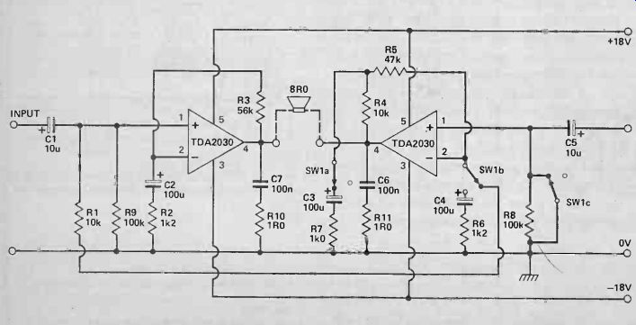
By using the TDA2030 IC audio amplifier it is possible to realize a hi-fi quality amplifier which will deliver 35 W with less than 0.1 % THD. This is done by using a pair of ICs in bridge and providing for use as a stereo amp by means of switching. The circuit is shown with the switching in the bridge mode. As can be seen, the amplifier requires a minimum of external components and these are only required to set the gain.
The amps are housed in T0220 package and must, of course, be mounted on a heatsink, preferably one with a thermal resistance of 3°C/W or better.
Organ Conversion
For IC Piano Martin Anderson, Oxford
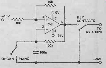
This simple oscillator circuit overrides the decay characteristics of the AY-1-1320 touch-sensitive piano IC to provide the infinite sustain of an electronic organ. In effect, it simulates hitting the piano key with great rapidity, such that the repeated note merges into a continuous sound. The circuit is short-circuit-proof, and can be switched to revert to the original piano sound. If the frequency of oscillation is lowered, a vibrato effect occurs. Conversely, raising the frequency might cause breakthrough into the sound circuits, causing an unpleasant background noise. The values shown have been found to work quite satisfactorily.
= = = =
Electronics Today (UK print magazine)
Also see: Link |