This power supply is suitable for the experimenter. It has fully adjustable output voltage and current limiting. A single meter can be switched either to voltage or current while an LED will indicate an overload.
-------------
SPECIFICATION---ETI 132
Output Voltage
Output Current
Current Limit
Load regulation
Line regulation
0-15 V variable
0-1 A approx 1.2 A
35 mV 0 to 1 A load
20 mV
220 to 260 V input
LED indication of current overload
---------------
THIS ECONOMICAL POWER SUPPLY replaces the ETI 111 supply published some years ago. The 111 gave an output voltage variable between 1.5 and 15 V, this project gives the full range 0 to 15 V. In addition this supply features metering (or you can use the calibrated scale on the second version if you don't have a spare meter) to enable accurate setting of voltage or current.
The 132 is attractively housed in a plastic case and Scotchcal front panels are available to give the unit a professional look.
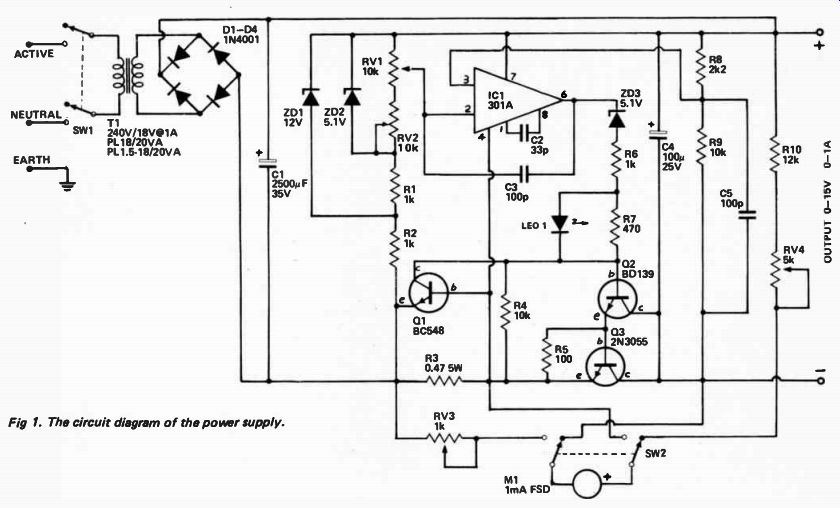
Fig 1. The circuit diagram of the power supply.
Construction
Commence by assembling the pc board with the aid of the component overlay diagram. The main filter capacitor C1 is normally a chassis- mounting type, out we mounted this satisfactorily by passing the lugs through the large holes in the pc board, bending them flush with the copper and soldering. Check the polarity of the capacitor before fitting, as it cannot be seen later. The transistor 03 is fitted, along with its heatsink, with the two mounting screws. No insulation is used between the transistor and the heatsink but pass a small piece of tubing over the base and emitter leads where they go through the heatsink, to prevent shorting. If the meter is not required RV3, RV4 and R10 are not used.
The front and rear panels can now be drilled. Note that the mounting bracket of the transformer has to be cut back about 12 mm on one end to allow it to fit easily. If a scotchcal panel is used it
------------
How It Works
The 240 V mains is reduced to 18 V in T1. This 18 V ac is then rectified by D1- D4 and filtered by C1 to give about 25 volts dc ( on no load). The voltage reference for the supply is ZD2, which gives about 5 V dc.
However, due to the large variation in voltage across C1 ( caused by load changes) additional regulation is used, incorporating ZD1, and the two circuits give the stability required.
The regulator is a 'series-pass' type with the positive rail common and the negative rail variable. We have done it this way to achieve outputs down to 0 V. The comparator IC (LM301) cannot work with its input less than about 2 volts above the negative rail, but it can work with the inputs at the positive supply rail. However this will not work with all types of op amp - so do not substitute the 301 with a 741 or similar.
The output of IC1 controls the output transistors, Q2 and Q3. A level-shifting zener ZD3 is used in the output of IC1 as its output cannot swing low enough. The output voltage is divided by R8 and R9 and is taken to IC1 which compares it to that set on RV1. IC1 then adjusts the drive to the output stage until the two voltages are the same. RV2 is used to compensate for variations in the voltage of ZD2.
In the event of an overload the voltage drop across R3 will forward bias 01, which will bypass current away from the output transistors.
This causes the output voltage to fall, the comparator sees this error, and the output of IC1 goes to the positive supply rail ( trying to compensate). 01 however will continue to bypass any extra current, holding the output current constant at about 1.2 A. However, the additional current out of IC1 will for ward bias LED 1 and it will indicate the overload.
With such high gain in the circuit additional frequency stability is needed and C3 and C5 provide this.
For metering, we simply use a 1 mA movement meter and measure the voltage across the output (via 810 and RV4) and across R3 ( current).
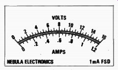
Fig 2. The meter scale used.
------------------------
Setting Up
1. Without Meter - With this version we rely on the potentiometer to be linear.
In practice it is not linear at the two ends of its travel. Calibration is done by adjusting the knob position and RV2.
Set the output to one volt and position the knob to read one volt. Now turn the knob to 15 V and adjust RV2 to give 15 V output. Recheck the 1 V setting and repeat the procedure, if necessary.
2. With Meter - Connect the output to an accurate voltmeter and turn the pot to maximum. Adjust RV2 to give 16 V. Adjust RV4 until the meter reads 16 V (with RV2 switched to volts). Now connect a load and an ammeter. Set 1A on the ammeter and then adjust RV3 until the power supply meter reads 1 A.
-------------
PARTS LIST
ETI 132
Resistors R1,2 1 k W 5% R3 0.47 S2 5 W 5% R4 10 k Y2W 5% R5 100 R6 1 k R7 470 R8 2k2 R9 10 k R10 12 k RV1 Potentiometer 10 k lin rotary RV2 10k Trim RV3 1 k " RV4 5k "
Capacitors C1 2500 µ electro type RG C2 33 p ceramic C3 100 p " C4 100 25 V electro C5 100 p ceramic Semiconductors D1-04 Diodes 1N4001 ZD1 Zener 5.1 V 400 mW ZD2 Zener 12 V 400 mW ZD3 Zener 5.1 V 400 mW LED 1 LED with mounting clip
Q1 Transistor BC548
Q2 BD139
Q3 2N3055 IC1
Integrated circuit LM301
Miscellaneous
PCB ETI 132
Transformer 240 V - 18 V 2A PI 18/20 VA or PL 1.5-18/20 VA Case PC1
Power cord and clamp Heat sink OSE H-3400 Two 2 pole 2 position 240 V Toggle switches Two terminals
Meter 1 mA FSD scaled 0-16 V, 0-1.2 A Knob
If meter is not required delete RV3, RV4, R10, the meter and one switch
---------------------
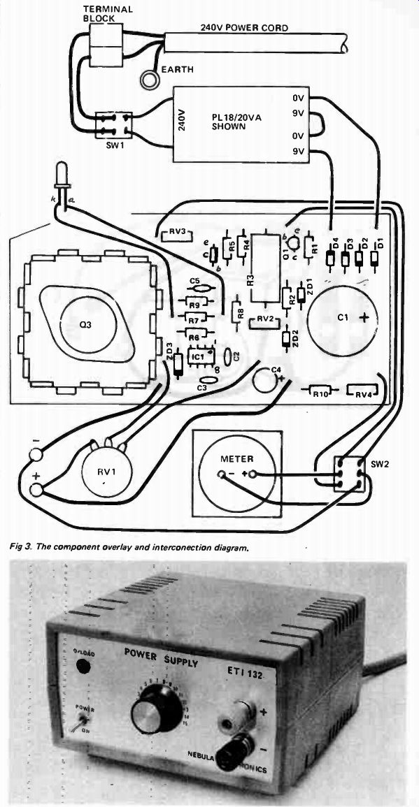
Fig 3. The component overlay and inter-connection diagram.
---------------
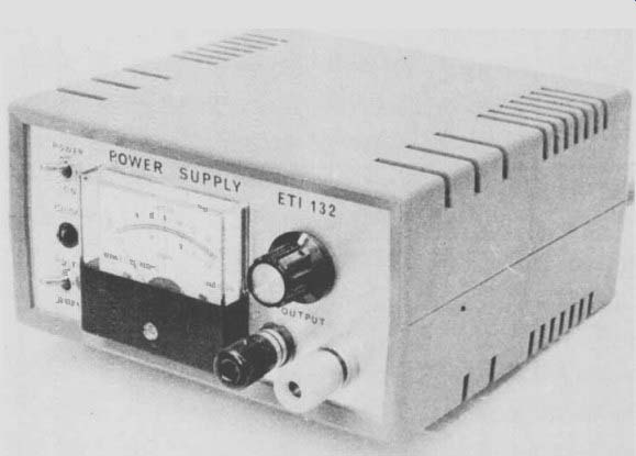
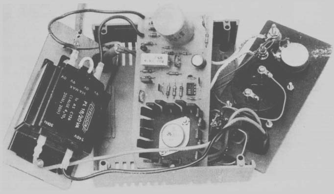
The photo on the right shows the second version of the power supply - where the voltage is set using a calibrated pot rather than a meter.
can be fitted before drilling and used as a template. Take care, however, not to scratch the panel.
Assemble the front and rear panels and wire the unit accordingly to Fig 3.
The wires to and from the power switch can pass the pc board via the chamfer on the lower left hand side. Other wires from the pc board to the front panel can be connected onto the copper side of the board.
-------------
SCOTCHCAL OFFER
Scotchcal panels ready to stick on are available from Electronics Today at $3.00 each. Send order together with a stamped addressed envelope - size at least 150 x 120 mm.
Address to Scotchcal Offer 132, Electronics Today, 15 Boundary Street, Rushcutters Bay, NSW, 2011.
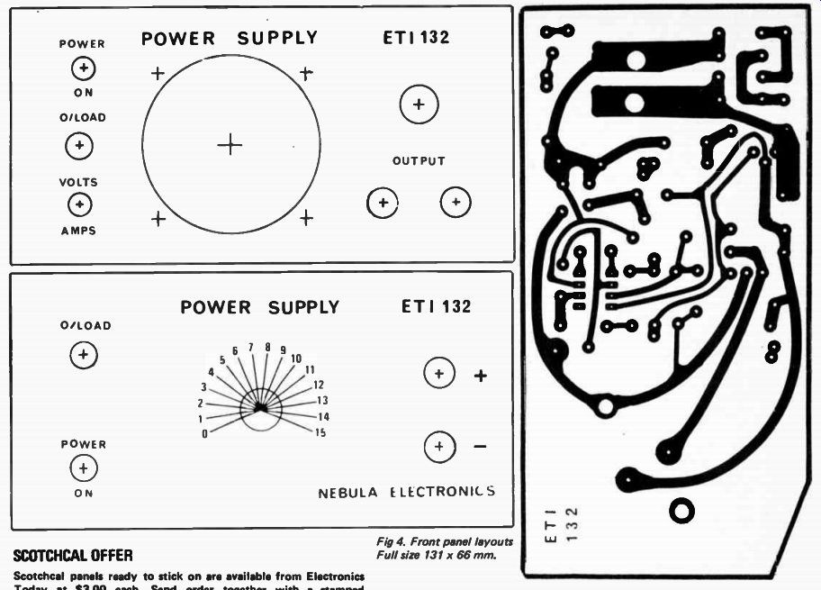
Fig 4. Front panel layouts Full size 131 x 66 mm.
Fig 5. Printed circuit layout. Full size 132 x 66 mm.
-----