Drive those TTL circuits with this 5 volt 10 amp ( max) supply.
WHILST the introduction of CMOS has lowered the power requirements of digital equipment using it, many large scale systems, because of cost and availability, are still designed around TT L logic. For such systems a five-volt supply having a capability of up to 10 amps is often required.
The choice of power supply for a system depends very much on the output requirements. In very low power applications a shunt regulator consisting of a series resistor and a zener may be entirely adequate. For medium power systems however a series-pass transistor regulator is normally used.
Whilst the series pass regulator is very good with regards to ripple and regulation the specification of the transformer is critical if the supply efficiency is to be above 50%. In a larger system this can be a very important factor.
With a switching regulator the requirements on the transformer are greatly relaxed and an efficiency of 70% or more can readily be obtained with mains-input variations of from 160 to 260 volts.
A fourth type is the switch-mode supply where the mains voltage is first rectified and filtered. The rectified mains then drives a high- frequency inverter which employs a ferrite transformer. Regulation is obtained by controlling the inverter and by this means very high efficiencies may be obtained. Nearly al i the components in such a system work at mains voltage and hence for safety reasons this approach was not used in our project.
CONSTRUCTION
All components, with the exception of the transformer and the choke are best mounted on a printed-circuit board such as the one specified. The choke should be wound as detailed in Table 2 with four layers close wound of 14 gauge B&S wire. Due to the dc current in the choke an air gap is necessary to avoid saturation. The easiest method of adjusting this gap for best performance is to run the supply at the maximum current required and adjust the gap by inserting that thickness of insulation between the cores which gives minimum ripple voltage. We found that a 3 mm gap was required at 10 amps for a ripple of 50 mV peak-to- peak.
-------------
TABLE 1
Comparison of typical series and switching regulators
SERIES SWITCHING
Output Voltage 5 V 5 V Output Current 10 A 10 A Efficiency
240 V in 50% 70%
260 V in 40% 70%
Ripple Voltage < 5 mV p-p 50 mV p-p
Regulation 0-10 A < 0.05 V 0.3 V
Input Voltage 240 ± 10% 160 to 260 V
Transformer Secondary 8.5 V @ 12 A 20 to 30 V @ 80 VA
Diodes Required 10 A 3 A
Filter Capacitor
33 000 µF
2 200pF
Short Circuit Current
15 A 15 A
-------------
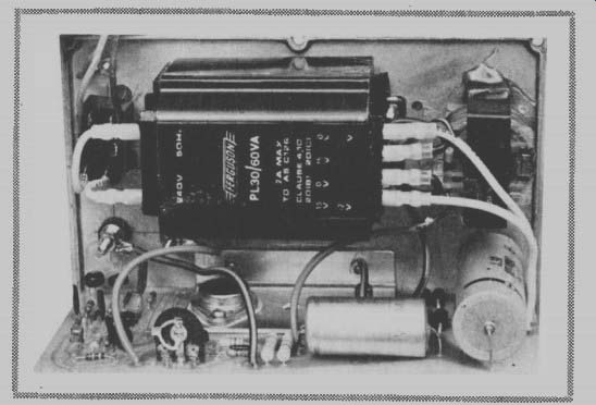
The prototype was mounted in a die-cast box which acted as the heatsink as well as a shield to prevent the radiation of RFI generated by the switching action of the supply. If another form of box is used a heatsink must be added to the transistor-diode bracket for cooling.
An external LC filter will reduce the ripple even further if required. For example a series choke of 20 turns of 1.6 mm wire on a 10 mm ferrite rod and a parallel combination of 1000 µF electrolytic and 0.47 polyester capacitors external to the box will provide considerable extra ripple attenuation.
---------
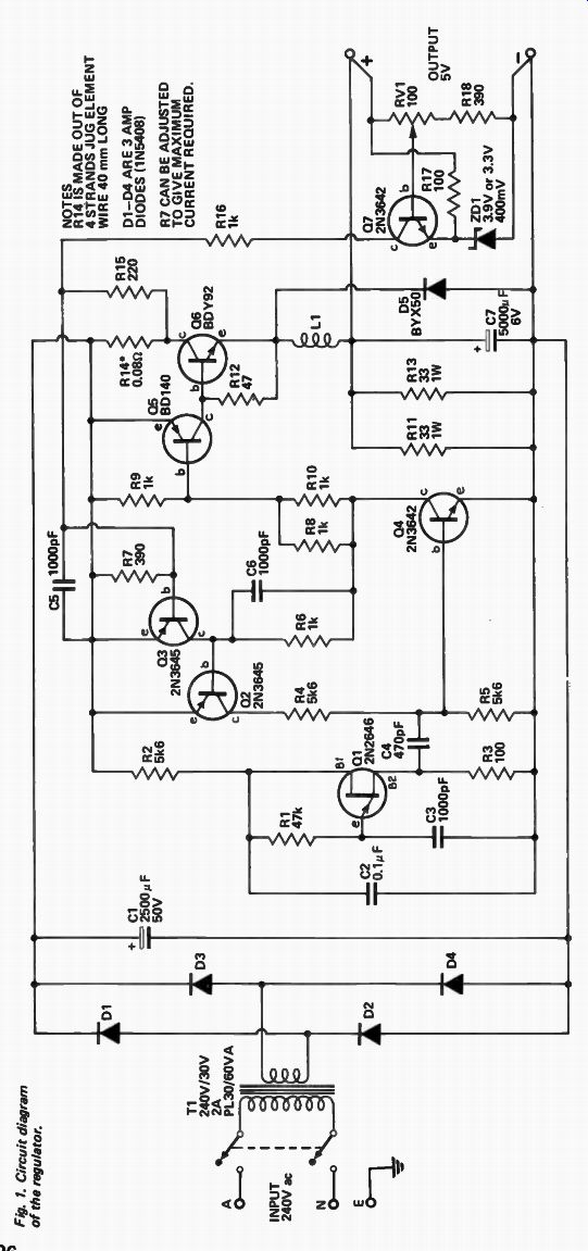
Fig. 1
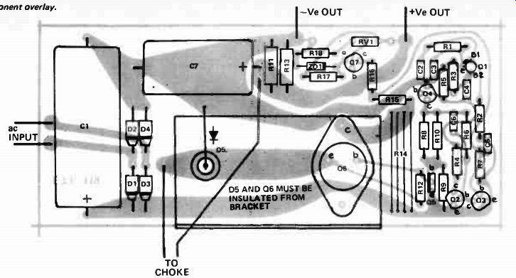
Fig. 2 Component overlay.
----------
PARTS LIST - Eti 119
R14 Resistor 0.0 n R11,13 " 33 1W 5%
R12 47 Ii2W 5% R3,17 " 100 1 / 2 W 5%
R15 220 1 / 2 W 5% R7,18 390 n 1 / 2w 5% R6,8,9 " 1k V2W 5% R10,16 " 1 k I/2W 5% R2,4,5 5k6 1 / 2 W 5% RI 47 k 1 / 2 W 5%
RV I Trim Potentiometer 100 n C4 Capacitor 470 pF ceramic
C3,5,6 " 0.001 uF polyester
C2 " 0.1 uF polyester
C1 " 2500uF 50 V electro
C7 " 5000uF 6V electro
D1-D4
Diode 3 Amp 100V IN5408 or similar
Q5 " BYX50-200
ZD1 Zener Diode
3.3 V or 3.9 V 400 mV Gil
Transistor 2N2646 or similar
Q2,3 " 2N3645 or similar
Q4,7 2N3642 or similar
Q5 " BD140 or similar
Q6 " BDY92 or similar
L1 choke see Table 1.
T1 Transformer 20V - 30V @ 60VA (7.5 Amp output)
75VA ( 10 Amp output)
SW1 Toggle switch 2 pole 240 V rated.
Heatsink bracket to Fig. 3 Diecast Box 6357p PC Board ETI 119 Insulation kit for Q6 and D5
* R14 Is made out of 4 strands of jug element each 40 mm long.
----------------
HOW IT WORKS
--- ETI 119
IN a conventional series regulator power supply the resistance of a series transistor is controlled in order to maintain the correct output voltage. The series transistor dissipates considerable power and therefore at very high load currents series regulators are quite inefficient.
In the switching regulator a series transistor is still used but does not operate in its linear range. Instead it switches ON and OFF at high speed such that the load is alternately connected and disconnected to a supply voltage that is higher than that required across the load. By controlling the ratio of ON to OFF time we effectively control the average voltage as seen by the load.
For example if it is on for 25% of the time the average output voltage will be 25% of the input. Thus by controlling the ON/OFF ratio the output voltage may be stabilized whilst dissipation in the series transistor is very greatly reduced.
However since most loads do not like their supply to be in the form of a square wave an LC filter is used before the load to pass only the dc component.
Referring to the main circuit diagram we see that transistors Q5 and Q6 are used as the series switch. L1 and C7 form the output filter.
Due to the inductance of the choke a flywheel diode is required, not only to protect the transistor, but to provide proper operation. When the switch is on, the load current flows through the transistor, the choke, and into the capacitor and the load (Fig. A). When the switch is opened the load current must continue to flow through the choke and this is done via the flywheel diode D5 (see Fig. B). The current through the choke will thus rise during the on period and fall during ' die off period.
The current never falls to zero except at very low load currents and the average is the same as the load current.
The operating frequency is set by the tiff Q1 which runs about 20 kHz; the higher the operating frequency the lower the ripple voltage on the output. However as the operating frequency goes up so also do switching losses in both transistor Q6 and diode D5. The 20 kHz was chosen as a compromise.
It is high enough not to be audible but low enough to keep these losses to a minimum. A fast transistor and diode are still required however. For example if an MJ802 transistor is used the power losses increase by 5 to 10 watts at 10 amps output current.
When the UJT fires the pulse generated is coupled into the base of Q4 by C4 turning Q1 on. This, in turn, turns on Q2 and the switch Q5/6.
When Q2 turns on Q4 also turns on and both latch on. If the current through Q6 rises above about 12 to 14 amps Q3 will turn on robbing current from the base of Q2 allowing both it and Q4 to turn off. This also turns off the output switch Q5/6.
This is the current protection circuitry.
A voltage proportional to the output is provided by RV1 to Q7 for comparison to the voltage of ZD1. If Q7 is turned on sufficiently it will also turn on Q3 thus unlatching Q2/4 and turning off the output switch.
Once the supply has stabilized this action will control the on time of the switch in each cycle of the 20 kHz, such that the output voltage is maintained at a voltage as set by RV1 in a smooth and even manner.
We used a 240 V to 30 V 2 A transformer, which is adequate for supply currents of up to 7.5 amps, however any transformer having an output of 20 to 30 volts and a power rating of 60 VA would do. If up to 10 amps output is required then a transformer with a rating of 75 to 80 VA would be required.
It is also possible to supply the regulator from a dc supply of 10 to 40 volts. If the voltage available is less than 20 volts R2 should be replaced by a link to ensure that the UJT operates correctly.
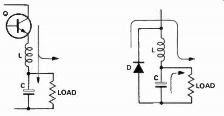
Fig. A. Current paths with switching transistor on. Fig. B. Current paths with switching transistor off.
--------------
--------------
TABLE 2 Choke winding details.
CORE Philips E core 4322-020 34720 two required
FORMER
Philips 4322-021 31830 or 4312-021 23622 one required
Four layers close wound of 1.6 mm wire core gap 3 mm (see text).
-------------------------------
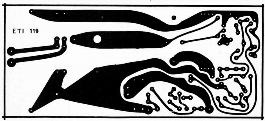
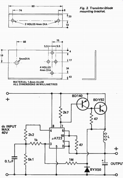
Fig. 3. Transistor/diode mounting bracket.
Fig. 4. This circuit recommended by a components supplier is simple but lacks short-circuit protection. Such protection is difficult to add to this circuit.
Fig. 5. Printed circuit-board layout. Full size. 178 x 78 mm.
--------------------