This updated version uses bigger and more readily available seven-segment displays.
THE ETI 533 DIGITAL DISPLAY WAS originally published in the July 1975 issue of Electronics Today and has been very popular as a general purpose display module. We are republishing this project for two reasons. Firstly, many people have asked for the details of how to use a larger display. And secondly, the type of display originally specified is now quite difficult to obtain.
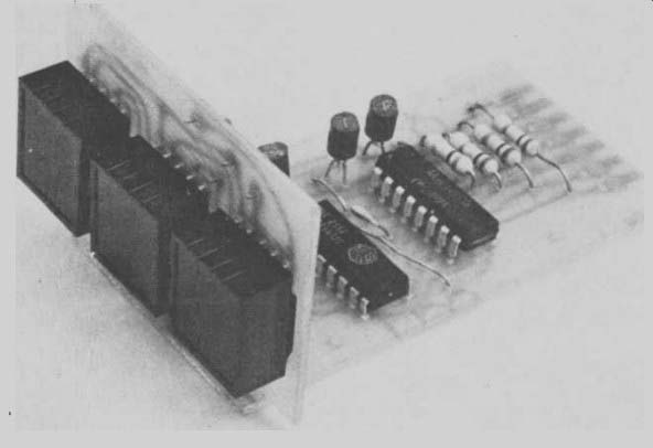
We therefore redesigned the display section of the module to accept the Fairchild FND 500 type of display which has 13mm high characters and is quite readily available. Of course the previous design is still quite valid and when the DL 704 and NSN74 type of displays are available they can be used as specified in the original article.
Only the small display board has been changed and it may be fitted to a previously built logic board if necessary. The new display board is, however, wider than the old board and the appropriate room must be available -- especially if two modules are to be mounted side by side.
Digital Display
All digital instruments have a common assembly in the display system. Again, almost all instruments require decade counters, stores and decoder-drivers for the display Normal systems using TTL logic generally have a 7490, a 7475 and a 7447 to drive each 7 segment LED display digit. Hence to build a three-digit display nine ICs are required in addition to three display ICs.
However, complex logic functions are available in CMOS which allow a 3 digit display to be built using only two ICs - and such ICs are available at reasonable cost. One of the devices is a three-digit, decade counter, store and the second is a three-digit decoder driver. Thus three digit displays can be built which have the following advantages:
1. Small size
2. Low power consumption ( 120 mA compared to 600 mA in TTL)
3. Wide power supply range (5-15V unregulated).
4. Cost about same as TTL but rapidly decreasing.
5. Immunity to noise is greatly improved.
Disadvantages: Maximum frequency about 1 MHz compared to 15 MHz for TTL.
Construction
Construction is quite straightforward especially if the printed circuit boards described are used. Since both ICs are CMOS devices, they can be easily damaged by static charges.
Hence they should be handled as little as possible, fitted to the board after all other components and soldered using a minimum of heat.
Starting with the display board use a short length of thin insulated wire to form the link which goes between the pins of the FND500 then add the displays.
Next fix lengths of tinned copper wire to each of the four holes on the bottom of the display board. Allow approximately 10 rim of wire to extend from either end of the holes.
Bend each wire so that they lie parallel and flush to the surfaces of the display board -- do not solder as yet.
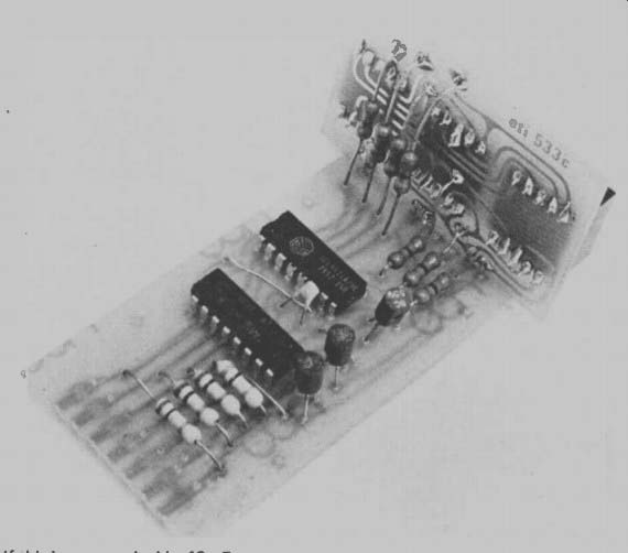
On the main printed-circuit board (533A) fit resistors R1,2,3,4, and R9 capacitors C1 and C2 and the three links.
now mate the display board to the main board by inserting each of the previously bent wires into its corresponding pair of holes on the main board.
Apply gentle force to the display board until its bottom edge fits snugly against the main board.
Solder each of the wires to both the display and main boards to make a sound electrical and mechanical support for the display.
Fit R5, 6,7,8, 10, and 11 and, taking care to orientate them correctly, fit Q1, 2 and 3 and IC1 and IC2.
Lastly check that all components have been correctly fitted and all solder joints are good. If possible get someone else to check your final circuit as a final safeguard.

----------------
PARTS LIST
ETI 533
R1, 2, 3, 4
Resistor 100 k R5-11
Resistor see text.
C1 C2
IC1 IC2
Q1,2,3
DISPLAYS
PC boards Capacitor 1n0 Polyester
Capacitor 10 n
Polyester Integrated Circuit MC 14553 ( CMOS)
Integrated Circuit 14511 or 4511 ( CMOS)
Transistor BC 558 or similar FND500 or similar.
Three required.
ETI 533A and ETI 533C
----------------
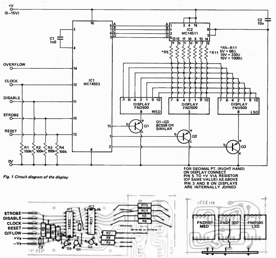
Fig. 1 Circuit diagram of the display.

Fig. 2 Component overlay of the logic board. FOR DECIMAL PT. ( RIGHT HAND) ON DISPLAY CONNECT PIN 5 TO +V VIA RESISTOR (OF SAME VALUE) AS ABOVE PIN 3 AND 8 ON DISPLAYS ARE INTERNALLY JOINED

Fig. 3 Component overlay of the display board.
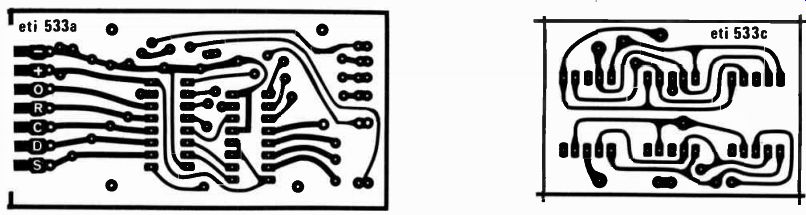
Fig. 4 Printed circuit layout of the logic board. Full size 78mm x 42mm

Fig. 5 Printed circuit layout of the display board. Full size 53mm x 36mm.
--------------
How it works -- ETI 533
The heart of the counter is 1C1. This LSI CMOS chip contains a three-digit decade counter, three sets of latches, and a three-digit multiplexer with an internal oscillator. C1 is used to set the frequency of this oscillator.
The four input lines to IC1 are used to control the operation of the counter.
Since 1C1 is a CMOS device R1-4 are used to protect its inputs. Pulses to be counted are fed to the clock input and on a negative transition the value in the counter is increased by one. The schmitt-trigger action of the clock input allows any value of transition time of the input pulse.
The counter operates when there is a low at the disable input ( pin 11). To ensure accurate counting the clock should be low when the disable is brought from a high to a low level. The strobe input controls the loading of the latch.
When it is low, data can be accepted for display. However, the strobe input has no effect on the counter, i.e., even with the strobe input high, the counter can still be incrementing.
A high on the reset input clears the counters ( to a 000 state) and stops the internal multiplexing oscillation of IC1, and so blanks the display. Returning the reset to a low allows the internal oscillator to start up and all zeros to be displayed.
All inputs are standard CMOS inputs and require a minimum voltage change of from 30% to 70% of supply volts.
However it is recommended that a swing from 0V to supply be used to give a satisfactory noise margin. Each input can be considered to be 100k shunted by 8-10 pF. Voltage swing below 0V and above supply are also to be avoided.
The one output available is the over flow ( pin 14). This goes positive when the counter is 999 and the clock input is high. When the clock input goes low and advances the counter to all zeros the overflow goes low. This is a CMOS output and will swing between supply rails. It is not recommended that the overflow output be used to drive TTL directly.
It can be used to drive a second 533 display to give a 6 digit readout if required.
The internal multiplexer of IC1 allows considerable saving in parts and board space. It allows a three-digit number to be transmitted over a single set of lines and it does this by leaving each digit on the output lines for a short length of time, before replacing it with the next digit.
Then after presenting all the digits once, it starts over again and repeats the operation.
IC2 is a CMOS, latch, BCD to seven segment decoder and driver, however for this application the latch is not used.
It converts the 4-bit BCD code into the seven-line code necessary to drive the display segments. It also provides sufficient current to drive the display.
If it is required that the display be blanked to save power the track to pin 4 on IC2 should be cut and pin 4 switched to either + V or 0V. If 0 the display will be blanked.
Although IC2 is coupled to all three displays, only one display is lit up at any one time. Thus when it is the turn of the most significant digit to be displayed IC1 presents that number to IC2 which decodes the number and presents it to the three displays, but only QI is turned on, so only the left most display lights.
Note that IC1 controls which number is being presented and which transistor is turned on. This is called multiplexing.
The switching between displays occurs so quickly that to our eyes the light appears continuous.
Resistors R5 to All limit the current to each LED display to a safe level.
Three different values have been given for these resistors. Select the value appropriate to the supply voltage that you decide to use, 68 ohms for 5 V, 330 ohms for 10 V and 1k for 15 V. Transistors Q1, Q2 and Q3 also act as current amps since only a limited amount of current can be taken from IC1.
Any voltage from 5V to 15 V can be used to supply the counter, however, a supply voltage of 15 V allows the counter to operate at its highest speed.
---------------
-------------
USING THE DISPLAY
Power Supply
5 to 15 Vdc (do not exceed 16 V)
Clock Input Counter is advanced on the negative edge of the clock input.
Speed of transition is not important.
Disable Input Must be low to enable clock to advance counter.
Reset Input Counter is reset to 000 if this input is high.
Strobe Input
If this input is taken high the display will remember the counter state at the time of going high. The counter can still be advanced, or reset without changing the display.
Overflow
This output is used to clock a second module to form a six digit counter. Or to clock any CMOS circuit as an indication of overflow. The output goes high when the clock input goes high and the counter is 999. It goes low when the counter advances to 000.
Note 1. If long leads are used pickup may occur which causes interference with normal action of the counter.
If this is suspected add a 10 nF capacitor across the inputs on the module Note 2. To use the decimal points provided on the displays connect pin 5 on the displays to the positive supply rail via a resistor which has the same value as those used for R5 to R11. A separate wafer on the range switch should be used to enable the appropriate decimal point.
--------------------