(source: Electronics World, Aug. 1963)
By HAROLD S. RENNE
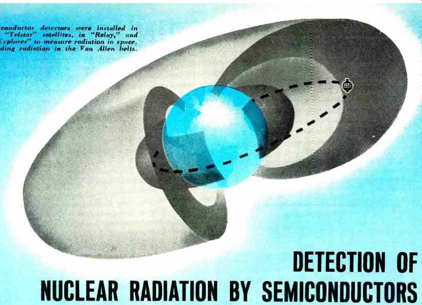
---Above: Semiconductor detectors were installed in both "Telstar" satellites, in "Relay'," and in "Explorer." to measure radiation in space, including radiation in the Van Allen belts.
In order for radiation to be useful, we must be able to measure it easily, precisely, and inexpensively. Semiconductors, especially silicon, are now finding wide application in this important field.
GREAT strides have been made in the field of nuclear science in recent years. Evidence of these advances is all around us--new nuclear per plants, ships, submarines -and a continuing growth in the uses of radioactive isotopes. And nuclear radiation itself--alpha, beta, and gamma rays--is being employed in industry, medicine, and agriculture on an ever greater scale.
Food preservation by means of nuclear radiation is rapidly becoming a reality. The Army is embarking on an extensive program of testing irradiated bacon for palatability and preservation. The radiation protects the bacon from spoilage for long periods without refrigeration. And in Canada, much of the potato crop is irradiated to inhibit premature sprouting, thus prolonging the storage period of this important crop.
In the field of insect control, the screwworm fly has been almost completely eradicated in parts of the country. This was clone by sterilizing male screwworms with nuclear radiation and then releasing them in infested areas. Similar techniques are being tested on many other insects with encouraging results -this may be a partial answer to the furor raised by Rachel Carson's book "The Silent Spring."
Horticulturists are using nuclear radiation to speed up mutations in plants in the interest of developing new strains that are more disease-resistant, produce larger crops, or have other desirable properties. This work has already paid off handsomely--in Michigan, a new strain of pea bean, called "Sanilac," developed by irradiation techniques, has almost completely displaced previous varieties because of its resistance to disease and larger yields. Florists now have greater variety of colored carnations, thanks to irradiation.
Industrial applications of both nuclear radiation and radioactive isotopes are legion. Radiation improves the properties of many materials, including some plastics, and gamma rays are used extensively for the nondestructive inspection of welds, castings, and the like. Radioactive tracers are widely employed, for example, in checking the wear on piston rings, locating leaks in pipes buried in concrete, checking the efficiency of washing machines, and in many other applications too numerous to mention. And nuclear power sources for satellites, remote weather stations, unmanned navigation buoys, and the like have been developed in which the heat resulting from the disintegration of a radioactive isotope, such as strontium -90, produces electricity directly through the use of thermoelectric elements.
In the medical field, significant advances have been made in the use of radiation to treat cancer and other diseases.
Radioactive isotopes are now fed to or injected in human beings, and the paths followed by these isotopes are checked in various diagnostic and therapy applications, such as a diseased thyroid. Selective radiation in various parts of the body can be carried out by administering radioactive isotopes which concentrate in the portion of the body under treatment.
Very precise, localized treatments can be administered in this manner.
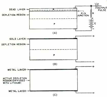
Fig. 1. Three basic types of silicon radiation detectors. (A) Junction,
(B) surface-barrier, (C) lithium-drift types.
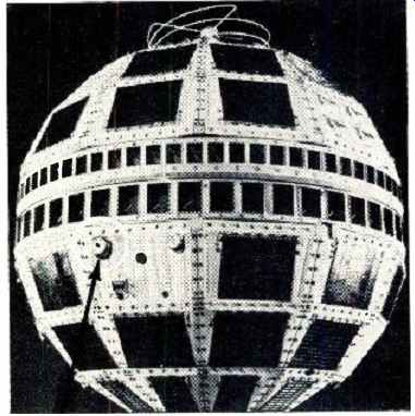
----The "Telstar II" communications satellite. There are
3600 solar cells on its surface. The two rows of microwave antennas around
the center receive signals sent up to satellite and relay them back to earth.
On the panel at left center, just below the antennas, is a silicon radiation
measuring device. An electron detector, it measures electrons in the range
of 750,000 to two million electron volts.
We could fill an entire book by merely listing the many applications of nuclear radiation. However, the foregoing examples will serve to drive home the point that this field is expanding rapidly and that it touches most of our lives in one way or another.
These examples also serve to emphasize another point. To be useful, we must be able to measure radiation easily, precisely, and inexpensively. It might be said that the usefulness of nuclear radiation bears a direct relationship to the ease with which it may be measured. For we must be able to administer precise doses in many applications, and must be able to measure these doses so we will know what has been administered. For these reasons, measurements in the field of nuclear science play an extremely important role in its application.
However, before we can discuss measuring equipment, we must know what we are trying to measure. The main products of a nuclear reaction, and the products which we want to measure, are alpha rays (helium nuclei), the beta rays (electrons), gamma rays, and neutrons. In some cases we want to measure the intensity of the radiation, that is, the rate at which it strikes an object or area. Devices for making such measurements are called "rate-meters." In other cases, we are interested in the total amount of radiation, or dosage, calling for an instrument which is known as a "dosimeter." In addition to knowing what we are measuring, we must have a standard to go by. The most commonly used unit is the roentgen (abbreviated r) which is defined on the basis of ionizing ability of the radiation in air. Multiples and submultiples of this unit are also employed. The megaroentgen (Mr) is a million roentgens, and the milliroentgen (mr) is one -thousandth of a roentgen. A total dose, or quantity of radiation, is then measured in roentgens.
If it is radiation intensity that we are concerned with, the customary unit is roentgens per hour (r /hr.) or, for low levels, milliroentgens per hour (mr /hr.).
Conventional Measuring Instruments
A number of different physical phenomena have been exploited in the measurement of nuclear radiation. These deal with the effects produced by such radiation on different materials. For example, there is the phenomenon of ionization--alpha, beta, and gamma rays will all produce varying amounts of ionization in a gas. The rays will expose photographic films--and will cause chemical reactions in various chemicals. In certain materials, flashes of visible light will be emitted when struck by radiation. The materials are then said to "scintillate." All of these phenomena have been utilized in commercial units now on the market.
Ionization. Geiger counters make use of a Geiger tube, which is nothing more nor less than a gas -filled tube with suitable electrodes for sweeping out the ions. Some measuring instruments use ionization chambers -again, a gas -filled chamber with an arrangement for removing the ions produced by the radiation.
Photographic Film. The fact that nuclear radiation will expose photographic film is the basis for an instrument known as the "film dosimeter." This instrument indicates the total dose of radiation received during the time the film is exposed.
The density of the developed film is a measure of the total exposure and, with proper calibration, the dose of radiation can be measured with a very high degree of accuracy.
Chemical Dosimeter. Chemicals of various kinds can be employed to measure the total dosage of nuclear radiation.
Certain chemical reactions take place under exposure, and the extent of these reactions is a measure of the total dose.
Changes in color, acidity, transparency, as well as other characteristics may be employed in order to determine total exposure.

Fig. 2. Nomogram for determining depth of penetration in silicon for particles
having various amounts of energy.
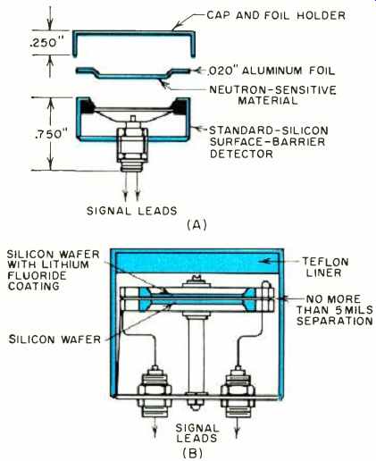
Fig. 3. (A) Cross-section of surface barrier detector for neutron detection.
Neutron-sensitive material is deposited on aluminum foil. (B) Fast neutron
sandwich detector.
Scintillators. In scintillation counters, the flashes of light which are produced by nuclear radiation are counted by a photomultiplier tube, together with suitable circuitry. The rate at which the flashes are produced gives an indication of the intensity of the radiations, and the total number of flashes indicates the total close.
Semiconductor Detectors
There are three main effects to be considered when studying the use of semiconductors in measuring radiation. First there is an effect which is very similar to ionization in a gas, namely, the formation of electron -hole pairs in the material.
Then there is the fact that semiconductors can become damaged when subjected to radiation. This damage is not the same as that suffered by the decoding transistors of "Telstar 1," where trouble was apparently caused by gas ionization within the transistor encapsulation. Finally, there is the phenomenon in which electricity is produced when radiation strikes a semiconductor diode -as in a silicon solar battery.
As mentioned before, nuclear radiation will produce electron -hole pairs when it passes through a semiconductor material such as silicon. Harnessing this phenomenon then involves removing these electrons and holes from the material before they can recombine, and then counting or measuring the number of "pairs" that have been formed. The use of silicon instead of a gas has a very great advantage in that for a given amount of energy lost by the incident radiation, approximately ten times as many charge carriers are formed. About 3.5 electron volts of energy are required to form one electron hole pair in silicon. The problem of sweeping out the electron hole pairs has been solved in a number of ways.
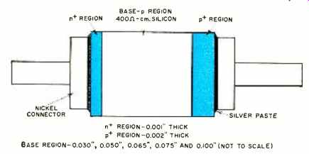
Fig. 4. An experimental silicon diode neutron dosimeter.
Junction Detectors
Application of an electric field to a material such as silicon can result in large leakage currents, since silicon is not a perfect insulator. However, by first forming a p -n junction in the silicon and applying a reverse bias, that is, applying a negative potential to the p region and a positive potential to the n region, the leakage current can be kept extremely small. Application of this reverse bias produces a "depletion layer" in the silicon. This is a region in which all electrical charges are swept out as fast as they are formed, and thus the region is, in effect, an insulator. See Fig. 1A. When a nuclear particle such as an electron or proton strikes this region, electron-hole pairs or ions are formed.
The impressed voltage then sweeps these ions to the appropriate electrodes, where they are collected and measured by suitable electronic circuitry. A single ionizing event would then cause a single pulse in the output, the size of this pulse depending on the number of hole-electron pairs that were formed.
Conventional techniques, such as diffusion, are employed in forming the pal junction. Slabs of ultrapure high-resistivity p-type silicon from 0.5 to 1 centimeter square are cut from a single crystal and are carefully cleaned and processed in the same manner as in the production of semiconductor transistors and diodes. The proper impurity, which may be phosphorus, is then diffused a very short distance into the surface, forming a thin layer of n-type silicon. Electrical contacts are then made to this surface layer and to the bulk material, and the detector is ready for operation.
It will be noted that electron-hole pairs formed in the surface it layer are not collected, and are lost. Therefore, every effort is made to keep this layer as thin as possible so that it will introduce a minimum loss. This so-called "dead" layer may be made as thin as 0.1 micron, so thin, in fact, that practically no hole -electron pairs are formed here, giving an essentially windowless detector.
The thickness of the depletion layer depends on a number of factors, the two most important being the resistivity of the p-type silicon, and the voltage applied across the junction.
It is desirable to get as thick a region as possible in most cases, so that the incoming radiation will produce a maximum number of hole -electron pairs. Thus, high-resistivity silicon is employed, and a high bias voltage is used.
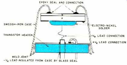
Fig. 5. Cross-section of vacuum-tight silicon radiation detector.
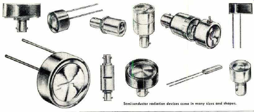
------ Semiconductor radiation devices come in many sizes and shapes.
Reports from Bell Laboratories indicate that diffused junction detectors have been fabricated with a depletion layer thickness of as much as 0.7 millimeter at 400 -volt bias. This is sufficient to stop a proton which has an energy of 10million electron volts.
Another factor to consider in the use of junction radiation detectors is their capacitance. The output signal energy of the detector is inversely proportional to the capacitance of the device. Thus it is important to minimize this capacitance to as great an extent as possible.
Surface-Barrier Detection
A highly satisfactory junction detector can be made by using the surface-barrier technique, as shown in Fig. 1B. Such detectors are formed by evaporating gold onto p-type silicon, forming a junction. When a suitable bias is applied, a depletion layer is formed as before, and the device functions in much the same manner as the diffused-junction device. Both techniques have been employed extensively in commercially available devices.
In surface-barrier devices, the radiation must penetrate the gold layer before it can be detected. Therefore, the layer is kept very thin--on the order of 150 angstroms--so there is essential]) no "dead layer" or absorption. The Oak Ridge National Laboratory has produced depletion layers as thick as 1.7 millimeters in its surface-barrier detectors.
Lithium-Drift Detector
For some applications, it is desirable to have a much thicker active layer than it is possible to achieve using either of the above techniques. Such devices might be necessary in measuring very penetrating radiation, such as protons in excess of 10-million electron volts. The lithium drift technique has been developed for producing thick layers ( see Fig. 1C) . Sensitive thicknesses of up to 5 millimeters have been reported.
In low-resistivity p-type silicon there is an excess of positive charges, or acceptors. By introducing carefully controlled amounts of lithium, these excess acceptors are compensated for and very-high-resistivity silicon and a large depletion layer result. The depletion layer can extend clear through the material. A big advantage of this device is that it can be operated at relatively low reverse bias voltages. However, it appears to be much more sensitive to radiation damage than the diffused silicon detector.
The detectors just discussed are not particularly suited to measuring gamma rays. Because of their penetrating power, such rays will readily pass through depletion layers of the thicknesses we have been discussing, forming few or no ions.
However, most fission products, including alpha rays, beta rays, protons, deuterons, tritons, and fission fragments can be easily measured. If the particle is completely stopped in the depletion layer, the size of the output pulse is a direct measure of its energy. Thus, with suitable instrumentation, the silicon detector can be employed to measure the energy of incoming particles.
The penetrating power of various particles in silicon is given in the nomogram of Fig. 2. If the energy and type of 'Particle are known, the range in microns can be determined directly. For example, the dotted line in Fig. 2 shows that a proton with an energy of 6 million electron volts will penetrate almost 300 microns of silicon.
Neutrons in general will pass through silicon without producing an appreciable number of electron-hole pairs. To use silicon diodes to measure neutrons, a "converter" layer is placed over the diode. This layer may contain lithium atoms, which react with neutrons to give a triton (isotope of hydrogen with an atomic number of 3) and a helium atom. These particles are then measured by the silicon diode. Typical construction for a device of this kind is shown in Fig. 3A. Sometimes, two silicon detectors are sandwiched together with a coating of lithium fluoride on one of the wafers. The basic detection principle is the same as before. See Fig. 3B. Silicon radiation detectors have a tremendous dynamic range, that is, they can be employed for measuring radiation intensities varying from a small fraction of a milliroentgen per hour, or a few counts per minute, up to the limit of available electronic equipment which can be on the order of hundreds of thousands of counts per second. Also, since the size of the output pulse can be measured, the energy spectrum of the incoming radiation can be determined. This can be extremely useful in identifying the specific radiation or identifying the radioactive isotope which is producing the radiation.
An interesting application of silicon detectors is their extensive use in measuring radiation intensity in space, including the Van Allen belts. Systems were installed in both " Telstar" satellites, in the "Relay" satellite, "Explorer XV," and others. With appropriate shielding and the use of magnetic and electric fields, these detectors have been used to count electrons, protons, and other charged particles of widely varying energies in areas of outer space.
Radiation Damage
Radiation can damage semiconductor devices--both diodes and transistors. Some work has been done in an attempt to utilize this phenomenon in developing a radiation measuring device, but as far as the author knows, no such device is commercially available.
Radiation damage acts to slow down the rate of diffusion of minority carriers in silicon. The current-gain characteristic of a transistor made of silicon depends on the rate of diffusion and, thus, by proper calibration, the change in current gain can be used to determine the total amount of radiation received by the transistor.
In a semiconductor diode, neutron radiation damage can result in a change in the forward current for a certain applied voltage, hence monitoring this current can give an indication of total radiation. The diode can then be employed as a neutron dosimeter. It is not necessary for the voltage to be applied continuously--it can be applied only when measurements are required. Readings can be taken as often as desired without affecting accuracy. An experimental diode of this kind is shown schematically in the diagram of Fig. 4.
Production of Electricity
Extensive tests conducted at Bell Laboratories indicate that silicon solar cells are very simple and useful devices for measuring high-intensity radiation. Cells of the n-p type are employed, as they are much more resistant to radiation damage than the formerly employed p-n type.
For most applications, it is only necessary to connect the solar cell to a relatively inexpensive microammeter. This microammeter can then be calibrated directly in intensity ( rads per hour, for example) . In a typical solar cell, an intensity of a million rads per hour of xor gamma radiation would produce a current of 37 µa. With more elaborate instrumentation, 100 rads per hour can be measured, and intensities as high as a billion rads per hour can be measured if the radiation that is involved is not too energetic.
Commercial Devices
We will now describe briefly some of the commercial solid-state radiation counters currently available from a few companies. It should be clearly understood that this section is by no means complete, either as to manufacturers or as to products. However, the descriptions will provide some indication of the type of semiconductor radiation detectors on the market.
Most of the devices made by Oak Ridge Technical Enterprises Corp. are of the surface -barrier type. A wide variety of depletion depths is available, including totally depleted units with thicknesses from 50 to 500 microns. All use a very thin gold electrode on the surface of n -type silicon. The devices can be employed for neutron detection using appropriate converter foils, such as lithium.
Some of the company's detectors are so constructed that they can be stacked for work requiring greater depletion depths.
Molechem, Inc. manufactures surface-barrier detectors with n -type silicon having a nominal resistivity of 1000 ohm cm., and capable of being operated at bias voltages of 200 to 500 volts and even higher for selected units, producing depletion lavers upwards of 1 mm. thick.
Units with very large active areas up to 2.2 cm are available. These detectors can be provided with an evaporated laver of lithium fluoride for neutron detection.
Solid State Radiations, Inc. makes silicon-junction detectors primarily. The p -type silicon with a resistivity of about 1000 ohm-cm is the base material and phosphorus is diffused into the surface to form a very thin layer, less than one micron thick. Some of the company's detectors have a coating which makes them sensitive to neutrons. Different coating materials are used, including boron-10, lithium-6, uranium-235, and others, depending on whether fast or slow neutrons are to be counted and to be measured.
Ferranti Electric, Inc. also specializes in silicon-junction detectors. The base material is p-type silicon having a resistivity of 5000 ohm-cm. and the n-layer is formed by phosphorus diffusion. A cross -sectional drawing of a typical unit is shown in Fig. 5. A bias as small as 10 volts in these units will produce a depletion layer which will absorb 10-million electron-volt alpha particles. Maximum operating voltages vary from 50 to 200 volts for the different units in each series.
Nuclear Diodes Inc. specializes in large-area silicon surface-barrier detectors, with active areas as large as 3.4 cm. in standard units. These detectors are made from nominal 300 ohm-cm n-type silicon. Also available is the lithium-drift detector. This unit can be combined with a conventional detector to form a system for determining the energy of the units and combinations of units which are included in the company's line.
This account has given a general, over -all picture of the uses which can be made of semiconductor materials, particularly silicon, in detecting and measuring nuclear radiation. There is much interest in this field at present, and it may be expected that great strides will be made in the near future, both in the improvement of present devices and in the development of new materials and techniques.
REFERENCES
1. Oak Ridge "Technical Enterprises Corp., P.O. Bos 485. Oak Ridge, Tenn.
2. Molechem, Inc., P.O. Bor 531, Princeton. N.J.
3. Solid State Radiations. inc.. 2261 S. Carmelina Ave.. Los Angeles 64. Calif.
4. Ferranti Electric. Inc.. Plainview. Long island, N.Y.
5. Nuclear Diodes inc. 1640 Old Deerfield Rd.. Highland Park. Ill.