(source: Electronics World, Mar. 1966)
By DONALD E. LANCASTER
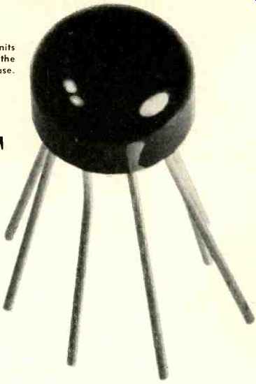
---------A new epoxy IC. Units have eight leads and are about
the same size as a TO-5 transistor case.
Some of the new integrateds have come way down in price and have many uses outside of computers. Here are techniques and circuits for these new IC devices.
THERE are two myths prevailing in regard to today's integrated circuitry. "Too expensive" and "only good for special computer circuits," are the hue and cry of many who simply do not yet realize the tremendous potential of in-stock integrateds applied to everyday circuits.
The facts are the exact opposite. Today there are very few basic circuits that cannot be fully integrated while substantially reducing the total cost, complexity, and assembly time. Improved reliability, temperature performance, and ruggedness are gained in the bargain. For instance, about $1.60 spent at a distributor's will buy the equivalent of three or four 2N708 transistors and five or six resistors, which separately might cost over five dollars, not counting the extra assembly time. For the same price, you also get an all-silicon circuit fully guaranteed and tested to operate over a specified temperature range into fully specified loads. This eliminates a large measure of the normal environmental testing, "burning in" of components, marginal resistance values, and expensive testing.
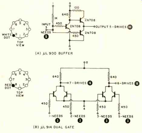
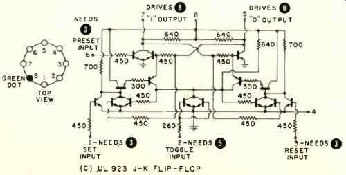
Fig. 1. Internal circuit of the three IC's described in text.
Of the twenty or so major integrated-circuit (IC) manufacturers, six have widely distributed, low-cost lines. Of these, the epoxy micrologic series of Fairchild Semiconductor lends itself well to our purpose of developing a number of basic integrated circuits that can be used for both commercial and experimental purposes. By obvious changes in supply voltages, impedance levels, and pin connections, these same basic circuits are pretty much applicable to other manufacturers' IC lines.
The Fairchild series consists of three integrateds packaged in eight-lead epoxy packages, the same size as a TO-5 case transistor. As a family, the units may be directly connected to each other. One supply voltage of +3.6 volts is specified, but any voltage from 3 to 4.5 should suffice for many applications. The latter is easily obtained from two or three pen light cells.
The pin connections are numbered counterclockwise from the top, with a color-coded dot directly beside lead 8. The units are specified over a + 15° to +55° C interval, useful for both room temperature and laboratory environments. Identical, wider-temperature units are available at premium cost.
Although sockets are readily obtainable, the breadboarding technique shown in the photo is a good means of mounting experimental circuitry. This technique makes all connections readily accessible and well separated. To mount the IC, eight Teflon press-fit terminals are pressed into holes forming a circle 3/4" in diameter. The leads of the IC are all bent radially outward and soldered directly to the tips of the terminals.
Printed circuits are impractical with integrateds unless two sided or multi-layer board is used; otherwise too many jumpers are required.
Rather than specify an input requirement as so many ohms or so many ma., and output requirements similarly, a much easier method is used on this IC line. Both input requirements and output drive capability are specified as so many "units," as indicated in the circles in the circuit diagrams. Any combination of inputs can be driven by an output whose drive capability exceeds the sum of the input units required. For instance, we will see that a AL914 requires "3" units of drive at an input and delivers "16" units of drive at an output. Thus one AL914 output can drive five AL914's inputs, with "1" to spare. All other requirements are determined in a similar manner, simply adding up the loads and keeping the load units equal to or less than the drive capability.
The three IC's are compared in Fig. 1. The AL900 ( about $1.60 each) is a buffer element designed to provide inversion and a high drive capability. This circuit finds use whenever a large number of inputs (up to a load factor of "80" units) is to be driven from a single circuit or when a low-impedance output is required for external circuitry. This three-transistor, five-resistor circuit operates as a switch. Ground the input and the top transistor saturates, connecting the output load to +3.6 volts which is tied to lead 8. 'Connect the input to a positive voltage between 1 and 3.6 volts and the top transistor goes off and the bottom two saturate, connecting the load to ground (tied to lead 4) through a low impedance.
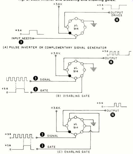
Fig. 2. Basic inverter and disabling and enabling gates.
A convenient method of mounting for breadboarding circuits.
The AL914 is called a dual two-input gate, but is far more useful than the name implies. It consists of two pairs of transistors sharing common collector loads. Outside of the supply and emitter connections, both halves of the circuit are completely separate. Considering one side, in the absence of any input, both transistors remain off, and the output voltage is equal to the supply voltage ( connected to lead 8). If either (or both) inputs go positive, the driven transistor (s) saturates, and the output is connected to ground (connected to lead 4) via the low impedance of a saturated transistor. This IC is the workhorse of the line, for it readily forms all the logic circuits, all multivibrators, a host of linear amplifiers, level detectors, and some others that we will shortly examine.
Fanciest of the three integrateds is the µL923-at about $4.00--a full-counting flip-flop. The IC is the equivalent of fifteen transistors and seventeen resistors. It singlehandedly counts by two, automatically steering its own input to the proper side every count, even at push-button speeds. This IC is also useful as a shift register or memory element and re places some complicated binary and ring-counter circuitry.
Inverter and Gate Circuits
In all the circuits, we have purposely left out the inner connections of the IC's to emphasize the external system connections and the simplicity of using integrated circuitry. To study the circuits from a discrete equivalent standpoint, refer back to Fig. 1.
The simplest circuit is the inverter of Fig. 2A. Here a bi nary "1" input produces a "0" output and vice versa. Use this one to invert any digital pulse or generate a complementary digital signal. The circuit functions on the presence or absence of base current in one transistor. A positive input signal saturates the transistor and grounds the output. A grounded input signal turns the transistor off and the output goes positive. If desired, the other half of the AL914 may be used elsewhere in the circuit.
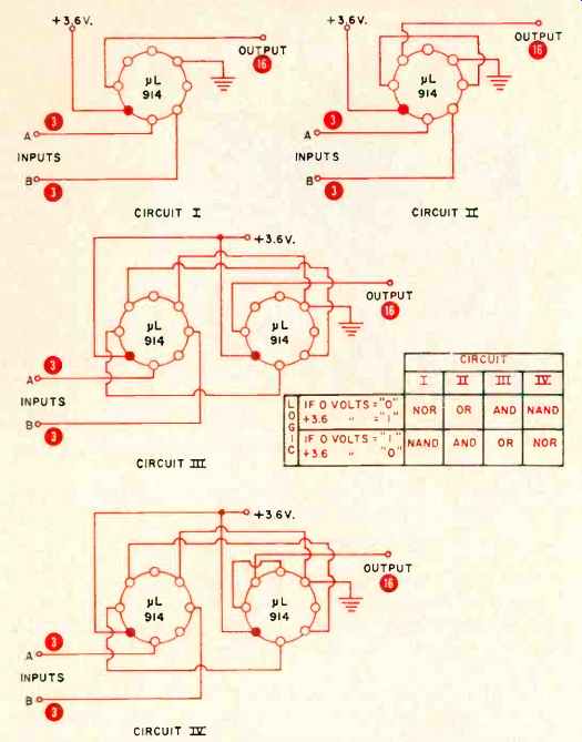
Fig. 3. Logic circuits along with their various designations.
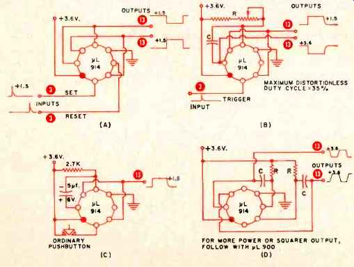
Fig. 4. (A) Set-reset flip-flop, latch, or memory. (B) Mono-stable, delay,
or gate generator. (C) Bounceless, noiseless push-button. (D) Astable oscillator
or square-wave generator.
Using both inputs produces the disabling gate of Fig. 2B.
Here the IC inverts the digital signal on lead 1 only if the input to lead 2 is grounded. A positive input at lead 2 grounds the output irrespective of the condition of lead 1, disabling the circuit.
If the opposite effect is desired, an inverter may be added to the gate input. Now, as in Fig. 2C, a grounded-gate input prevents any signal inputs on lead 1 from being inverted and appearing at the output. If the gate input, lead 3, is made positive, the inverter stage makes leads 6 and 2 grounded and thus passes the input signal. This is then an enabling gate.
Logic Circuits
There is always so much confusion over just what constitutes and "and," an "or," a "nand," or a "nor" circuit for, depending on how things are defined, one circuit can perform any two functions. In binary arithmetic, there are only two possible system states, the "one" state and the "zero" state. The rules for logic are simply:
If any "one" input produces a "one" output, the circuit is an "or" circuit.
If any "one" input produces a "zero" output, the circuit is a "nor" circuit.
If all input "one's" have to be present to produce a "one" at the output, the circuit is an "and" circuit.
If all input "one's" have to be present to produce a "zero" at the output, the circuit is a "nand" circuit.
Note that all the rules are defined in accordance with the presence or absence of "one" inputs. There is nothing in the rules that concerns itself with "zero" inputs.
The trouble comes in when a "one" and a "zero" are defined in a system. Circuit people will usually define a "one" as a positive input and a "zero" as a grounded input; the computer people will often do the exact opposite. Four basic logic circuits are shown in Fig. 3 along with a chart which defines the logic operations in terms of your choice of what a "one" or a "zero" is.
Circuit I produces a grounded output if either input is positive and a positive output only if both inputs are grounded.
Circuit II produces a positive output if either input is positive and a grounded output only if both inputs are grounded.
Circuit III produces a positive output if both inputs are positive and a grounded output if either input is grounded.
Circuit IV produces a grounded output if both inputs are positive and a positive output if either input is grounded.
These logic circuits are the very basis of all digital computer circuitry and other areas where particular sequences or coincidences must be detected.
Multivibrators
All the conventional multivibrators (flip-flops) are easily built using the connections of Fig. 4. In 4A, the output of one half of a FL914 is connected to one input on the other half and vice versa. The two remaining inputs, one on either side, are brought out for external connections. This produces a bistable multivibrator or a set-reset flip-flop. A momentary set pulse consists of a positive signal briefly applied to lead 1.
This momentarily grounds lead 7, the output of the set inverter. The grounding of lead 7 grounds lead 3 which lets lead 6 go positive. The positive output of lead 6 is connected to lead 2 which holds the multivibrator in the set state after the input trigger disappears. A reset pulse applied to the opposite input will transfer the output to the reset side, again holding itself in the new state until the next arrival of a set pulse. This circuit is useful as a latch or memory as well as a gate or interval generator.
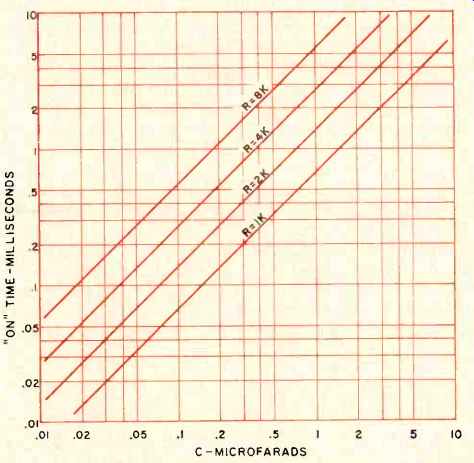
Fig. 5. Performance of the monostable circuit in Fig. 4B.
If one of the feedback connections is broken and a capacitor and recharging resistor are inserted in its place, the monostable multivibrator of Fig. 4B results. Here a set or trigger input pulse changes the state of the flip-flop, but it changes state back again after a time delay determined by the recharging time of capacitor C. When the input trigger arrives, lead 7 immediately goes to ground. The charge on C cannot instantaneously change, so C drives lead 5 negative, turning off the other side of the flip-flop and providing feed back to hold the output in the set state. R then slowly recharges C, making lead 5 more and more positive until finally lead 5 is positive enough to turn on its transistor and revert the state of the monostable back to normal. The net effect is a constant time interval or delay, in the form of a rectangular pulse, produced every time an input trigger pulse arrives.
Fig. 5 includes a family of curves that lets you choose values of C and R for required time delays. Varying R with a potentiometer gives control over the delay interval. The de lay is largely independent of the supply voltage. The circuit will only operate on a 75% maximum duty cycle, and the duty cycle should be held to less than 30-35% if timing accuracy is important. For instance, a 300-microsecond multivibrator must have at least 100 microseconds to recover. If timing accuracy is important, it should have at least 700 microseconds; otherwise the earlier arrival of new trigger pulses will affect the timing interval.
One example of a monostable application is the noiseless push-button circuit of Fig. 4C. Ordinary push-buttons are both bouncy and noisy. In the first few milliseconds of con tact, the contacts may alternately make and break as many as several hundred times. This is detrimental to any high speed electronic circuit that faithfully follows every input pulse. With the monostable, the first bounce triggers the circuit and produces a single 15-millisecond pulse. Only one output pulse is produced for every depression of the push button.
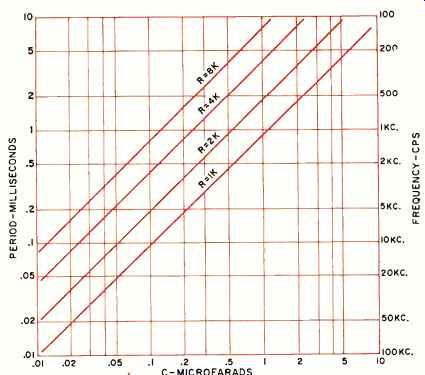
Fig. 6. Performance of the astable circuit in Fig. 4D.
If both multivibrator sides are capacitively coupled and resistor-recharged, an astable or free-running circuit results (Fig. 4D). This one is useful as an oscillator or square-wave generator. It may be synchronized to external signals by applying sync pulses to leads 1 or 5. Fig. 6 gives the period and frequency of the astable circuit for various R and C values. Again, the timing is largely independent of supply voltage, for an increasing supply voltage simultaneously increases the stored charge and recharging rate.
For a squarer output or a lower output impedance, a AL900 may be added to Fig. 4D. Another possibility is to start with two AL900's and two capacitors and use the internal 1000-ohm recharging resistors by jumpering leads 1 and 8.
Special Circuits
A Schmitt trigger or level detector is made using the circuit of Fig. 7A. This one has the interesting property that the output abruptly snaps from a grounded to a positive output or vice versa the instant a slowly varying input voltage exceeds a critical value. The circuit is essentially an emitter-coupled multivibrator with emitter-current feedback provided by an external 27-ohm resistor. For the circuit to possess snap action, the voltage drop across this resistor should be less after triggering than before. This is brought about by unbalancing the collector loads with an external 820-ohm collector resistor. With this resistor, the voltage required to trip the trigger is somewhat above the voltage required to keep the trigger in the "on" state. 'This feature, called "hysteresis," prevents the trigger from "chattering." Changing the values of the external resistors will vary the amount of hysteresis and the trip points.
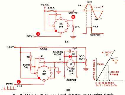
Fig. 7. (A) Schmitt trigger, level detector, or squaring circuit. (B) Frequency-to-voltage
converter, tach, or frequency meter.
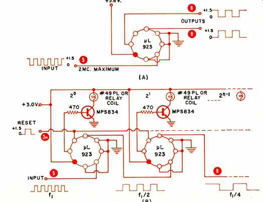
Fig. 8. (A) Divide-by-two, binary scaler, or counting flip flop. (B) A
self-indicating, resettable binary counter.
Another interesting variant is the frequency-to-voltage converter of Fig. 7B which consists of a monostable followed by an integrating capacitor. This circuit makes an excellent tachometer or pulse counter and, when preceded by the Schmitt circuit, a very useful analog frequency meter at low cost.
The converter is always run at less than about 30% duty cycle to give a linearity of better than 2%. Each input pulse trips the monostable. The meter is selected so that it reads full scale when the ratio of monostable "on" time to total interval time is 30%. If the total interval time were doubled, the duty cycle would be only 15%, the meter would only read half scale, and so on. The choice of C and the meter determines the range of operation. Calibration is achieved by using the 500-ohm calibration potentiometer. A zero adjuster serves to buck out the slight zero offset of the saturated IC.
Diode D1 protects the meter from damage should a pulse rate higher than full scale appear at the input. If desired, the integrated output voltage may be amplified and then employed for additional purposes.
Binary Counters
A divide-by-two or binary scaler is shown in Fig. 8A. Here a single AL923 is used as a counting flip-flop. No additional circuitry is required to properly steer the input pulses to the correct side of the flip-flop. The pulses at the input may be any waveshape and can appear any time from one per hour up to 2,000,000 pulses per second. The fast response of this circuit makes noise less push-button operation (as in Fig. 4C) mandatory when operating off mechanical contacts.
These IC's may be cascaded to form a counting chain, frequency divider, or binary counter simply by connecting output to input down the line. This produces a series of output square waves whose repetition rates are 1/2, 1/4, 1/8, 1/16, etc. of the input. Driver transistors and either pilot lights or relay coils may be added in order to indicate the condition of each stage, as shown in Fig. 8B.
Linear Circuits
Many digital integrated circuits make fine linear amplifiers. The basic circuit is the differential amplifier or "long-tail pair," formed out of a single 4914, as shown in Fig. 9A. The emitter resistor and the negative supply voltage form a current source that splits its current to either side as the difference of input signals. Signal A sees an emitter-follower working into a grounded-base amplifier to arrive at the output; signal B sees only a common-emitter stage. The output of B is inverted, but that of A is not, so the difference (A-B) appears at output.
This amplifier configuration is one of the most reliable and stable, but is not used too often with discrete circuitry for two reasons. First, two transistors are required per stage. Second, and more important, the forward voltage characteristics of the two transistors must be closely matched and held at exactly the same temperature, otherwise the bias points will shift with temperature and the differential amplifier will become unbalanced. This requires a controlled environment and expensive matched pairs of transistors. With integrateds, this is no problem at all. Both transistors are of identical geometry side by side on the same slab of silicon. They must al ways be at an identical temperature and must be nearly matched.
For instance, Fig. 9B shows a wide band amplifier, useful from d.c. to 7 megacycles. Input B is grounded. The output consists of input A amplified by approximately 26 decibels and in phase with the input. Adjusting the bias potentiometer establishes the d.c. operating point at the output and sets the stage gain. The output impedance is less than 1000 ohms; the input is greater than 3000 ohms, so stages may be cascaded for more gain. If capacitor coupling is used, resistors must be added shunting each input ( at most 1000 ohms) to keep the non-linear input impedance from charging the coupling capacitor and improperly biasing the circuit.
Transformer coupling is preferable.
If tuned transformers are used, the selective r.f. amplifier of Fig. 9C results.
Here the gain is 30 decibels and the center frequency may be anything from audio to above 20 mc. (with gain falling off somewhat above 10 mc.). The value of the LC ratio and the tuning capacitors will determine the bandwidth, selectivity, and the center frequency. Stages may be cascaded for more gain. It is desirable to invert the phase every stage with the transformer connections to minimize the possibility of oscillation.
The gain is controllable by an a.g.c. voltage input of 0 to-3 volts from a source impedance of 1000 ohms or less.
This gives the astonishing gain-control range of 30 db of gain to 50 db of loss for a total of 80 db.
Inputs less than 150 millivolts will be linearly amplified; above this level the amplifier limits sharply. This property makes this circuit very attractive for self-limiting 10.7-mc. i.f. amplifiers.
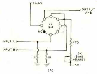
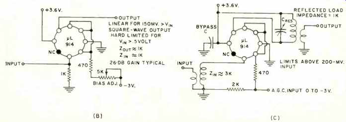
Fig. 9. (A) Differential amplifier or signal comparator. (B) D.C. to 7-mc.
amplifier, limiter, or square-wave generator. (C) R.F. amplifier or FM
limiter useful to 20 mc., with a 30-decibel gain figure.