By LOTHAR STERN and IRW N CARROLL, Semiconductor Products Div. Motorola Inc.
Long-lived and low-power solid-state devices are starting to invade the fields presently served by incandescent lamps and glow-discharge display tubes. Used as light sources, light modulators, indicators, displays, detectors, couplers, and sensing arrays, here's what's available now and future prospects.
above: This 7-segment solid-state readout is a custom hybrid unit
with 4 the decoder-driver IC chip (top) mounted in the same package.
FOR some time, two technologies have been moving along separate but gradually intersecting paths. Now that their courses are destined to meet, this could produce a wave of new applications. The two technologies are optics and electronics and the relatively new term--optoelectronics--coined to describe this merger, has captured the attention and fired the imagination of scientists, engineers, technicians, and experimenters.
The field of optoelectronics deals mainly with the twin phenomena of converting light into electric current and, conversely, turning an electric current into light. Neither of these is new. The phototube and the solid-state cadmium sulphide photocell are early and successful examples of light detectors while tungsten-filament and gas-filled bulbs have been serving as light sources for many years. But all of these components have limitations that restrict their use to rather mundane applications. Only the relatively recent development and mass production of silicon photodetectors and light-emitting semiconductor diodes, combined with large-scale integration of their required electronic circuitry, have lifted these restraints. Today, although the actual utilization of these new optoelectronic devices is still minimal, the variety of optoelectronic products in mass production is large enough to move the technology from experimentation to implementation. Moreover, there exists a custom-product capability so that the only limitation on applications will be the imagination of the equipment design engineer.
Light-Emitting Diodes
In electronic equipment, incandescent and neon lamps will soon have strong competition from light -emitting (semiconductor) diodes (LED's) in applications ranging from indicators to displays. And the reasons are obvious.
For a start, the response of LED's is many times faster than that of previous devices. While incandescent lamps work very well at d.c. and respond even in the low audio-frequency e range, LED's can faithfully follow frequencies well into the megahertz region. Also, solid -state devices are much less fragile than their glass counterparts. Finally, their anticipated lifetime is far greater. While the life of an average incandescent indicator bulb may reach 5000 hours and that of an average neon lamp could extend to 10,000 hours, it is estimated that the life expectancy of an LED is on the order of 20 to 30 years. (Some special incandescent and neon lamps have life expectancies as great as ten times the previous figures. -Editor) In addition, high-volume manufacturing techniques are expected to quickly establish price levels for solid -state devices that are competitive with today's well-established and mass-produced incandescent lamps.
Most of today's light-emitting diodes are either made of gallium arsenide, which produces infrared radiation (approximately 9000 angstroms) when the diode is forward biased, or of gallium arsenide phosphide which produces a visible red light of about 6600 angstroms. Both are being manufactured in quantity and both have specific applications. The visible-light diodes are designed to be used as panel lights, circuit-condition indicators, light modulators, displays, and the like. Infrared emitters are recommended for card and tape readers, for shaft and position encoders, and for other applications where photodetectors can take the place of the human eye.
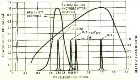
Fig. 1. Relative response of silicon photodetector compared to wavelength of
light output produced by various light-emitters.
Since the infrared wavelength of gallium arsenide coincides with the optimum response for silicon detectors, this provides a system of optimum efficiency (Fig. 1). Although the variety of light emitters is limited at the present time, engineers are using packaging variations to broaden the scope of their application. Each of the various packages may house the same emitter chip, but the shape and materials used in the package determine device characteristics--and its price.
One inherent characteristic of light-emitting diodes is the linear change of light intensity with current. The limiting-current value is set by the power dissipation capability of the package in which the die is housed. Thus, an efficient heat -dissipation package permits operation at higher current, hence greater light output. Moreover, the shape of the package determines spatial radiation distribution (Fig. 2).
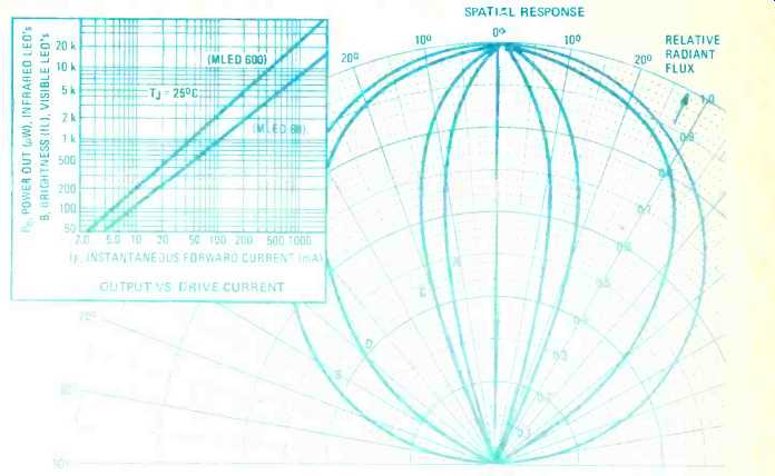
Fig. 2. The power or light output of two typical LED's for various forward
currents. Also shown are four spatial responses available.
From a materials standpoint there are three different package types: plastic, metal, and ceramic. The metal packages are generally hermetically sealed and have a lower thermal resistance than the plastic units. Thus, they are suitable for use over a higher temperature range and can be operated at a higher maximum current. As a result, they can produce a brighter light output. On the other hand, the plastic -packaged devices are considerably less expensive and are usually preferred in commercial, industrial, and consumer applications. Ceramic packages are currently being used for readouts of the seven-segment type.
But this is only the start of differences. Of the two Motorola packages, it would appear that the primary difference is one of size. This, however, accounts for some rather startling variations in spatial response--and in subsequent applications. In the small package, the chip is near the center of the curved dome so that emission of light radiated at an angle is at a maximum. Hence, the angle of visibility is quite wide, making these devices suitable as pilot lights, fault-indicators, and in other wide-angle-visibility applications. In the larger package, the die is mounted some distance from the dome. This results in internal reflections that produce a rather narrow beam. Visibility is therefore limited to a relatively narrow angle, although the output is less diffused and appears brighter. This type of unit is better suited for "directional" applications such as modulators, tuning indicators, optical data links, and the like.
Similar considerations apply to metal-cased units so that careful evaluation of the unit's spatial emission characteristics is recommended before making a final selection (Fig. 3).
Monolithic 5 x 7 alphanumeric GaAsP light-emitting diode array.

Fig. 3. Some currently available light-emitting diode packages, together
with some of their important operating characteristics.

Fig. 4. Silicon photodetectors are available as diodes, transistors,
Darlington amplifiers. Typical specs are indicated.
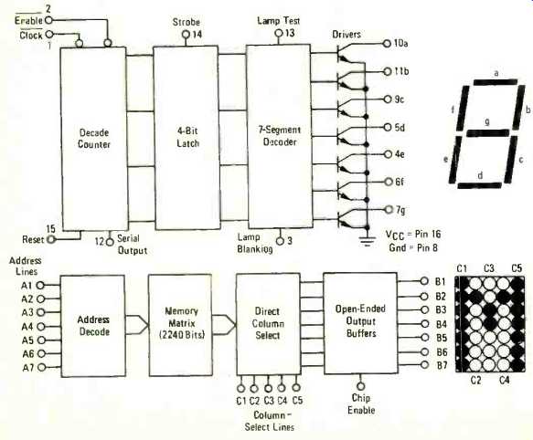
Fig. 5. (Top) Combined counter-latch-decoder-driver and 7-segment readout.
(Bottom) Circuitry needed for 5 X 7 dot matrix.
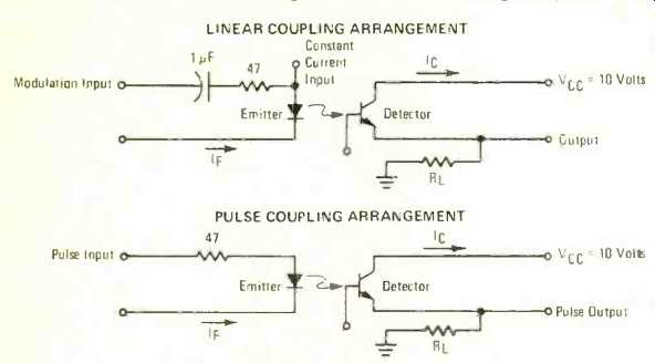
Fig. 6. The circuit arrangements that can be employed with opto-electronic
couplers for linear, analog-type signals or For pulses.
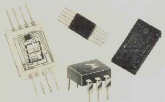
above: Across the top are three 7-segment readouts showing different
packaging techniques. Unit at top center has red cover and one at right
is on black background, thus obscuring display segments in both cases.
Device at bottom center is optoelectronic coupler.
A group of optoelectronic detector arrays. The large device is 100-diode
monolithic array; smaller ones are standard arrays.
Photodetectors
The susceptibility of semiconductor-device characteristics to impinging light has been known since the earliest days of the technology. Indeed, the variations in leakage current in glass -packaged diodes, due to changes in light levels, was a nuisance that was corrected only at considerable extra expense. Yet, it is this phenomenon that is being exploited for light-sensing purposes and today's semiconductor photodetectors are designed to optimize this effect.
Silicon photodetectors are widely available in three electrical configurations: diodes, transistors, and Darlington amplifiers. Each successive variation produces an improvement in sensitivity, but at the expense of speed (Fig. 4). The different characteristics of these variations make them suitable for different applications. The photodiodes, with their extremely fast (nanosecond) response, are ideal for laser detection as well as for ultra-high-speed demodulation, switching, and decoding. Their low current (microamps) output, however, makes subsequent amplification necessary.
Phototransistors, on the other hand, have respectable outputs in the mA region, but their switching times are measured in microseconds. Accordingly, they are more suitable for industrial inspection, processing, and control systems. To increase their versatility, such devices are available in miniature as well as subminiature packages, the latter being recommended for tape and card reading, character recognition, and other applications requiring high density mounting.
Finally, the photo Darlington transistors have outputs high enough to act as industrial drivers, but speeds that are limited to several hundred microseconds.
The Impact of LSI
The explosive growth of solid -state optoelectronics is greatly enhanced by maturing large -scale integration (LSI) capabilities. Not only from a size standpoint, but from power-supply requirements as well, both technologies are entirely compatible. It is this compatibility that provides new potentials for widespread implementation. For example, the mere replacement of an incandescent or neon-lamp readout with a solid-state unit might not be of sufficient importance to warrant an equipment redesign. But the concomitant reliability improvements, space reductions, and cost advantages could provide an ample incentive.
A case in point is the combined counter-latch-decoder-driver circuit (Fig. 5) which, in conjunction with a hybrid-type LED readout, provides this kind of advantage. Moreover, an integrated-circuit chip can be placed in the same package with the readout for a fully operative, single-package digit. Such devices have been produced, but are not yet generally available.
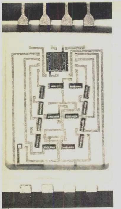
Another LSI circuit for potential use in conjunction with solid-state readouts is the MMOS -1 2240 -bit character generator. This circuit can generate the outputs required for 64 different USASCII characters to be displayed on a 5 X 7 dot matrix of light-emitting diodes.
Clearly, the combination of circuit and display arrangements offers a number of possibilities for compact portable equipment which would not be feasible without these interlocking technologies.
Optoelectronic Arrays
Like other semiconductor components, discrete opto-electronic devices, such as combined light-emitting diodes and photodetectors, have many uses. But their real potential lies in optoelectronic arrays which, like complex integrated circuits, are apt to gravitate toward custom designs.
There will be, and indeed already are, a significant number of standard arrays. But these are produced more to demonstrate functional capability and manufacturing proficiency than an expected high-volume sales potential.
Of course, there are exceptions. Certain light-emitting displays (i.e., 7-segment readouts) do represent a huge market for standard parts; so do punched-card and tape-reading assemblies for standardized computer equipment. Many products for these functions have already emerged. But large as these specific markets are expected to be, they are nothing at all compared to the potential offered by custom designs.
An overall glimpse of what is imminent and the possible impact on future designs, is best obtained by looking at some of the products that are now, or soon will be, available.
Optoelectronic Couplers
An excellent example of optoelectronic utilization to replace conventional electronic components is the optical coupler. Consisting of an infrared-emitting diode coupled to a phototransistor in a single package, the device advantageously replaces interstage transformers and relays as well as coupling and feedback networks.
Consider as an example the MOC1000 coupler. The unit can be used as a linear-signal coupler or transformer and as a pulse coupler or relay (Fig. 6). In the former mode, a constant current supplied to the light emitter biases this diode and, since the output (infrared in this case) is directly proportional to the diode current, any increase or decrease of diode bias current resulting from an applied modulation input, causes corresponding variations in light output.
These are coupled to the phototransistor detector which provides an equivalent linear output current. In this particular device, the output current is typically 60% of the input current and the bandwidth is 700 kHz. Other devices, with an emitter-detector current gain greater than unity, are now available on a limited basis.
As a pulse coupler, the device requires no bias current. The detector is either "off" (with a dark-current of typically less than 20 mA) or "on" (with a maximum continuous forward current of around 35 mA). Used as an electronic relay, it is fast--much faster than mechanical relays--and it has no contacts to "bounce," pit, or corrode. It is small, insensitive to vibration, and unlike other forms of electronic relays, its output is completely isolated from the input.
Obviously, couplers of this type could be produced with a wide variety of gain, sensitivity, and output current.
Light-Emitting Displays
The cold -cathode gaseous display has been "king of the hill" for so many years that it is familiar to everyone working with digital electronic equipment. Now, however, its reign is being threatened by solid-state optoelectronic read-outs that offer a number of advantages.
Optoelectronic readouts are smaller than their gaseous counterparts. Their numerals are only 1/8" to 1/4" high, compared to over 1/2" for the latter. Yet, they are so clear, sharp, and easy to read that they appear to be larger. Moreover, their bright red color makes them easily visible and distinguishable at a respectable distance. They operate at low voltage which makes them more compatible with transistors and integrated circuits than are gaseous displays.
Optoelectronic displays come two ways--monolithic and hybrid. The monolithics are smaller but less expensive. They are designed for instruments, calculators, and other indicators read at short and medium distances.
Hybrids are better suited for distance viewing, as in panel readouts. There's even work going on in combining the optoelectronic readout with all the associated electronic circuitry in a single package, so that each digit will be a complete, self-contained entity.
Sensing Arrays
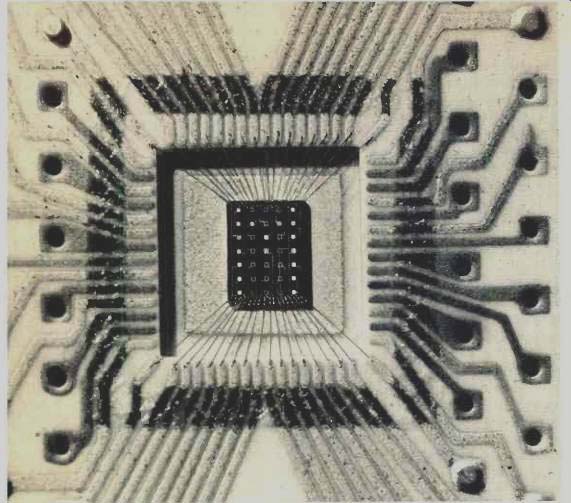
Individually packaged photodiodes and phototransistors can be board-mounted in large numbers to form discrete-device arrays. The smallest packages can be spaced as closely as 85 mils, but that's not nearly close enough for a great many applications. For extremely high-resolution requirements they are available as standard monolithic arrays of up to 39 photodiodes or photo-transistors in a single package, while custom monolithic arrays can include more than 100 devices. In a typical array, the diode chips are spaced on 5-mil centers with the active-element area per chip being 4.5 by 5 mils.
These arrays are designed for optical pattern and character-recognition equipment, mark sensors, and a wide variety of other sophisticated and critical applications.
Nor is this necessarily the optimum or maximum array size. On a custom basis almost any linear or two-dimensional design can be obtained for special purposes, including star-pattern recognition for navigation.
Some special sensor arrays being produced for standard off-the-shelf availability include card and tape readers. Currently, Motorola is producing 10- and 12-cell arrays with standard card spacings (0.087" and 0.250 ", respectively) and 9-cell arrays with 0.100" spacing for tape reading. These arrays consist of individually packaged cells that have been carefully matched for uniform sensitivity and then subsequently repackaged in array form.
From these, it is but a short jump to corresponding light-emitting arrays.
Since standard light-emitting diodes are individually housed in the same type packages as light sensors, they can be molded in the same type array forms as the detectors to assure a perfect match.
The Green Light
To date, materials used for most semi-conductor light-emitters have been gallium arsenide (GaAs) and gallium arsenide phosphide (GaAsP)--for infrared and visible red light. There is, however, a strong demand for a green-light emitter, not only for the psychological impact of green light, but also because the eye is far more sensitive to green.
Green light can be obtained most readily from gallium phosphide (GaP), a material that is more difficult to process than GaAsP, but its advantages far outnumber its drawbacks. The first difficulty encountered is that of crystal growing. Because gallium and phosphorous have greatly differing vapor pressures, crystal pulling must be carried out in a special crystal "puller" capable of operating at pressures of 1500-psi (100 atmospheres). The importance of GaP is due to its dual nature--it can be used for red -and green-emitting devices, depending on the dopants used.
As a red emitter, GaP is more efficient than the more common gallium arsenide phosphide. However, the eye is not as responsive to the GaP characteristic wavelength so that apparent visual response is approximately equal for both types.
One significant advantage of GaAsP over GaP (as a red emitter) is that GaAsP devices exhibit a linear relationship between light output and current input up to very high current values.
Therefore, such units can be pulsed at high currents to yield an apparently high output (as long as power dissipation is kept within the thermal capability of the die and package). Gallium phosphide, on the other hand, saturates very quickly at increased current levels, with the resulting light output reaching a fairly constant value.
Although GaP devices of either red or green light are now in short supply, GaP holds promise of being the material of the future. The role of GaAsP could well be like that of germanium devices--there will always be some cases where it will prove to be the best choice.
-----p49 "Now don't worry, if something doesn't work right, remember--it's still in the design stage."
==============
Inside the LED
Of all the light generated in an LED, only a small fraction actually reaches the outside world. There are two basic factors that account for most of these losses: the low transparency of the LED material to the wavelength being emitted and the high index of refraction of the LED material.
A few of the possible paths that the generated light can take are shown in the illustration. The longer the path through the material, the greater will be the absorption of the light. As can be seen, light leaves the junction in all directions. The gold backing used for bonding reflects light emitted towards the back of the die adding somewhat to the forward-emission radiation.
The "bending" of the light being emitted is due to the high index of refraction of gallium arsenide phosphide as is the light being reflected from the inside surface back into the die.
If the light strikes the surface at an angle greater than the critical angle θc, it will be reflected back into the die.
The critical angle can be increased by placing the die in a material which has an intermediate index of refraction such as epoxy or plastic. Additional shaping of the plastic can also enhance the radiation characteristics.
Even when the generated light strikes the surface in an ideal manner, perpendicular to the internal surface (normal incidence), a certain portion of the radiation is reflected back into the die. This is due to the reflection coefficient which is also a function of the index of refraction.
The reflection coefficient can be reduced by coating the surface of the die with a transparent material that has an intermediate index of refraction. The thickness of this coating should be an odd number of quarter wavelengths of the emitted light as measured in the intermediate material. A common material is SiO2, while SiO or Si3N4 is also being used.
A combination of die-coating and encapsulation in an intermediate material can improve bare -chip efficiency by a factor of 2 or more. In addition, using a red plastic encapsulation that will pass the emitted radiation improves viewing contrast.
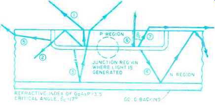
LEGEND:
1 . Directly emitted ray from top surface
2. Internally reflected ray from top surface
3. Specularly reflected ray leaving top surface
4. Diffusely reflected ray
5. Ray leaving side of chip
6. Ray with normal incidence with dotted line showing effects of reflection coefficient
7. Ray striking top surface at critical angle θc, and emerging ray parallel to surface.
=============
(adapted from: Electronics World magazine; Jul. 1975)
================