By JON L. TURINO
Simple, step-by-step design technique that can be used to produce this versatile sine-wave audio oscillator.
THE phase-shift oscillator has been around a long time. It is a versatile circuit which has a number of applications other than its main use as a sine-wave source in the audio-frequency range.
For the experimenter, however, there is usually one drawback to incorporating the phase-shift oscillator in a project--how do you design one that will work and oscillate at the frequency you need? Circuit designers use a long, mathematically complex procedure when they design a phase-shift oscillator; and then have the circuit built and tested to determine the actual parts values and to evaluate its performance. Many use an additional sophisticated technique unavailable to most of us--computer aided design (CAD). The phase-shift oscillator design procedure presented here is a simple, straightforward, step-by-step method for obtaining a circuit that will work when power is applied to it. The frequency of oscillation will be within five percent of the calculated value, and the d.c. stability of the circuit is entirely adequate if a low-leakage silicon transistor is used as the active element. The approximate frequency range of this phase-shift oscillator circuit is from 20 Hz to around 50 kHz.
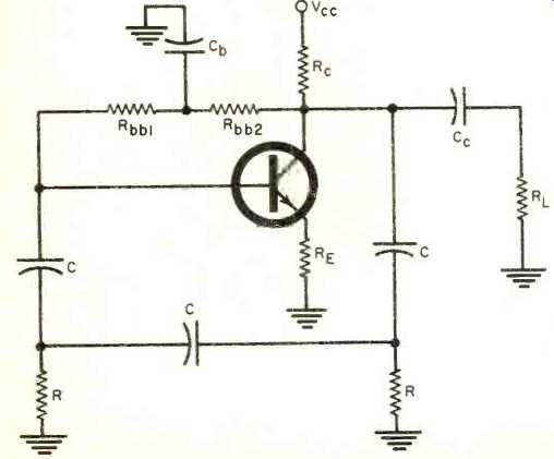
Fig. 1. Schematic of general type phase-shift oscillator circuit.
Fig. 1 is the schematic of the general circuit and the design procedure used to determine the parts values is listed in the box. Since the main stumbling block is in the first step, a little time is devoted to determining how to specify RL if the oscillator is to drive an amplifier or emitter-follower stage, as is usually the case.
Fig. 2 shows two typical transistor stages that might be used to isolate the oscillator from the actual load so that variations in the load will not affect the frequency or output amplitude. The input impedance of the emitter-follower stage (Fig. 2A) is actually the load resistance for the oscillator. Its value can be closely approximated using the formula Rin= (RB x ßRE) /(RB +ßRE) where ß (beta) is the forward current gain of the transistor, usually called hfe. For the stage in Fig. 2A, this value is 25k ohms.
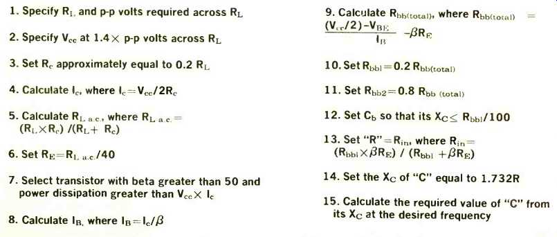
Determining the input resistance of the amplifier stage in Fig. 2B is slightly more complex. The effects of both RBI and RB2 must be taken into account, since they are actually in parallel with the transistor input. The formula for finding Rin for the circuit of Fig. 2B is Rin =1/ (1 / RB_1) + (1/ R_B2) + (1/ßRE). Once the load resistance has been determined, the rest is easy. Let's do an actual example. Suppose we need 10 volts r.m.s. at 5000 Hz and the emitter-follower of Fig 2A is used for isolation. Referring to step 1 of the design procedure, specify RL as 25k ohms and 28 V p-p across it (p-p is 2.8 times r.m.s.). The power supply (Vcc) must be 1.4 times 28 V, or about 40 volts. Now set collector resistor R, to 0.2RL or 5000 ohms.
For the stage to operate properly, the collector current must allow about one-half the supply voltage to be dropped across R, . Using the formula of step 4, 4 will equal 40 /2x 5000 or 4 mA. Now another composite parameter is needed. The a.c. signal from this oscillator sees both R, and RL in parallel as a resistance, RL e.,.. From the formula in step 5, RL ac. = 4100 ohms.
In order to sustain oscillation in this circuit, the voltage gain of the circuit must equal the loss through the phase-shift network. This loss can be mathematically reduced to a constant--37. Adding an eight percent "fudge factor" to this gives us the number 40. The voltage gain in the circuit of Fig. 1 is approximately equal to the ratio of the a.c. collector resistance (RL a.c.) to the emitter resistor, RE, so this relationship can be used to calculate the value of RE. In our example, 100 ohms is the closest standard-value resistor that will work properly.
Now a suitable transistor must be selected. First, it must be of a low-leakage silicon type. Second, it must have a beta (hfe) of at least 50 at the frequency at which we want the circuit to oscillate. Third, it must have a power dissipation of at least 40 V x 0.004 amp or 160 mW. One other important parameter is the collector-to-emitter breakdown voltage. It must be at least equal to the supply voltage, and preferably 50% higher. For our application, the 2N930 will work. Its beta is typically 100 all the way to 10 MHz, its power dissipation 300 mW, and its breakdown voltage a minimum of 50 V. Using /3=100, calculate the base current, 'B, at 0.04 mA. The formula in step 9 derives an Rbb (total) of 490k ohms.
The nearest standard value of Rbb1 and Rbb2 (from steps 10 and 11) are 100k ohms and 390k ohms, respectively. Now bypass the a.c. signal that would be fed from the collector to the base using this bias method so that it does not reduce the gain of the circuit. Cb is the bypass capacitor and its reactance should be less than or equal to 1000 ohms (Rbb1/ 100, step 12) at 5000 Hz. A 0.033uF capacitor does the job effectively.
Now the Rin for the oscillator stage must be determined.
This value is found using the same formula used for the emitter-follower input resistance, with Rbb1 substituted for RB (step 13): Rin= (100k X100 X100) /(100k+100 X 100) or 10k ohms. The value for the two "R" resistors in the circuit are now known.
In order for the circuit to oscillate, the signal applied to the base must be 180° out-of-phase with the collector signal.
Since we have three legs in our phase-shift network, each should provide 60° of phase shift. This occurs when the capacitive reactance (Xe) of the capacitors is 1.732 times the resistance of the "R" resistors. Therefore, Xc must be 17.32k ohms at 5000 Hz. Using the formula C =1 /2 pi f Xc, the value 0.0018 µF is derived and the design is complete.
Fig. 3 shows the complete circuit, with parts values assigned. When breadboarded, it provided 30 volts p-p output at 4900 Hz, very close to what was specified.
The frequency of oscillation can be trimmed to an exact figure by adjusting the value of either "R" resistor. The phase-shift oscillator provides a signal suitable for use as a code-practice oscillator, a fixed-frequency audio-signal generator for testing amplifiers and other audio equipment, and, with minor modifications, an active bandpass filter. It can even be used to generate the sound of bongo drums by making RE large enough so that the circuit gain is just below the point where oscillations begin. If a trigger is applied to the base of the transistor, the circuit will be shocked into oscillations which will quickly die away.
(Three such circuits at low, medium, and high frequencies, will create the sounds of a bass drum, a tom-tom, and a bongo drum, respectively.) The same gain-reducing technique (raising the value of RE) allows the circuit to become an active bandpass filter, an application the author has incorporated into a five-channel stereo color organ.
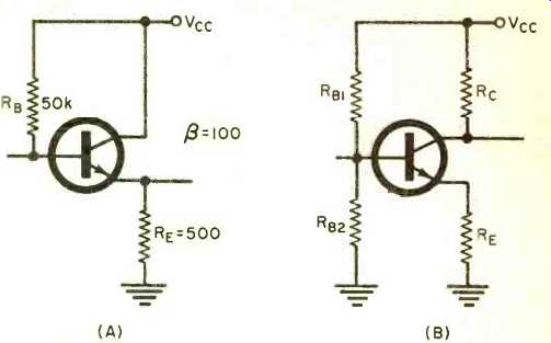
Fig. 2. Schematic diagrams of (A) simple emitter follower and (B) more
complex circuit that might be used to isolate the phase-shift oscillator
from actual load.
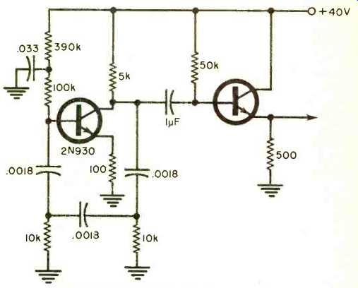
Fig. 3. The complete schematic diagram of the phase-shift oscillator
circuit constructed by the author showing the values of all of the various
components used.
above: DESIGN PROCEDURE
(adapted from: Electronics World magazine; Jul. 1975)
================