(source: Electronics World, Dec. 1971)
By FRED W. HOLDER
Operation of a new, highly sensitive radiation detector for low-energy protons and electrons that is being used in space exploration.
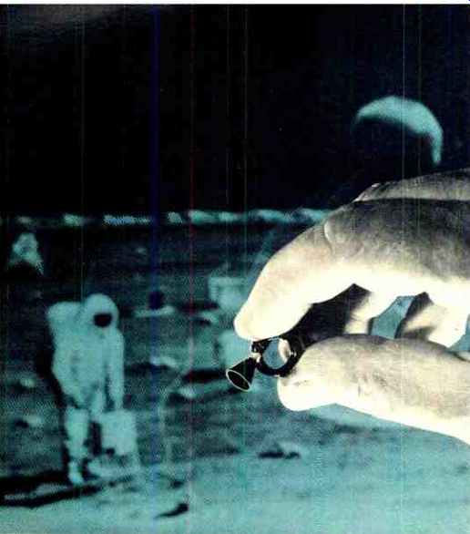
ABOVE: This tiny Channeltron, with its funnel opening, was used to detect charged particles in Apollo lunar environmental experiment.
It has always been difficult to detect low-energy photons and charged particles (electrons and protons) because these particles are so easily absorbed by matter only fractions of a micron thick. A new device, the channel electron multiplier (CEM), now makes this instrumentation task easier. The device was developed by the Bendix Research Laboratories, Southfield, Michigan. Called Channeltron, these patented units are capable of increasing the flow of electrons more than a million times so that charged particles received at the input can be measured by conventional electronic counter circuits.
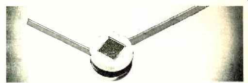
The CEM is adaptable to most low-level radiation measurements in the 1500to 2angstrom region of the spectrum, the ultraviolet and soft x-ray region. They have been used extensively in space exploration. For example, one circular model slightly larger than a quarter was designed for rocket-probe investigations of auroral plasma. Another model, coiled like a spring with funnel-shaped input, was the principal active element of the charged particle lunar environment experiment carried to the Moon by Apollo astronauts.
Similar to Photomultiplier Tube
Since operation of the channel electron multiplier tube is based on the same general principles as the photomultiplier tube, it is a good idea to first review its operation. The photomultiplier tube is an amplifying photoelectric cell having a number of electrodes called "dynodes." Each of the dynodes is maintained at a positive potential higher than the light-emissive cathode. Also, each dynode is maintained at a higher positive potential than the preceding dynode. See Fig. 1A. The photosensitive cathode of the photomultiplier tube emits electrons when light strikes its surface. These emitted electrons are attracted to the first dynode where they cause secondary emission as they strike the surface of the dynode.
The electrons emitted by secondary emission, greater in number than the original group leaving the cathode, are attracted to the higher positive potential of the second dynode. Here, again, they cause secondary emission as they strike the surface of the dynode. The growing number of electrons are swept away to the next dynode until they are finally collected by the anode. By repeating this process of current amplification ten or more times, an anode current greatly amplified from the original current at the cathode is obtained.
If the photomultiplier tube is to be operated in the high vacuum of space, an evacuated tube would not be necessary. The cathode could be exposed directly to bombardment by photons and charged particles or the first dynode could be given a special coating and exposed directly to bombardment by photons and charged particles arriving at the tube. See Fig. 1B. Electrons emitted by the dynode as it is bombarded are swept away to the second dynode to start the amplification process.
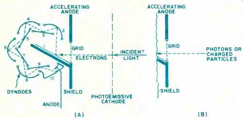
Fig. 1. (A) Operation of the photo-multiplier tube. (B) By removing photoemission
cathode, tube amplifies external charged particles.
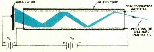
Fig. 2. Simplified diagram of channel electron multiplier. The CEM is
electrostatic device with a continuous dynode surface.
Such a photomultiplier tube would be designated a windowless radiation detector. The windowless detector is more efficient than the window type. The window-type detector must dissipate the energy of the particle in a medium capable of producing ionized atoms, free electrons, or emitted light quanta proportional to the energy of the particle. The result is often a feeble electrical signal of the same magnitude as the preamplifier noise.
Something Better Was Needed
Something better was needed to detect single electron events; the channel electron multiplier was the answer. Being windowless, the sensitive input of the CEM is accessible to all particles irrespective of type and energy and is especially adaptable to detecting single electron events with a very low count rate (one count in 100 seconds). The upper count rate limit is a few thousand counts per second before current saturation occurs.
Unlike conventional electron multipliers having a series of discrete dynodes, the CEM is an electrostatic device with a continuous dynode surface. Actually, the CEM is a small glass tube with an inner surface coating of high-resistance semiconductor material which serves as the dynode. See Fig. 2. A high voltage is applied across the length of the tube so that an electrostatic field exists within the narrow (one millimeter) channel of the tube. A charged particle or photon entering the tube opening will be accelerated along the channel until it strikes the dynode surface.
When this happens, secondary electrons are emitted from the semiconductor material. They are swept along at an accelerating rate by the electrostatic field until they also strike the dynode surface, creating an avalanche of electrons in the tiny channel. The gain in electron flow, caused by the avalanche effect, is limited to about 100,000 if the tube is straight. The limiting factor is the ion feedback resulting from a loss of electrons in the semiconductor material. Bendix scientists discovered, however, that bending the tube prevents this feedback and allows typical gains up to 10^8 electrons per input event.
These high-gain OEM's are often bent into helixes or "C "shaped structures to eliminate ion feedback and to satisfy packaging constraints. As shown in Fig. 3, typical electrical connections of the CEM may take one of two basic configurations: separate collector or cap collector. If the separate collector is used, it will be spaced about one millimeter from the end of the channel and have a collector voltage of 200 to 300 volts. The cap-collector configuration does not require an additional power supply, but develops the pulse signal across a load resistor RL. The cap collector can be metal foil bonded to the CEM with conductive adhesive. The h.v. power-supply voltage can range from 2000 to a maximum of 4000 for the model illustrated. Fig. 4 shows the gain curve for this unit, operated in the separate collector configuration, with different levels of high voltage and a collector voltage of 220 volts. As shown, the gain does not increase as rapidly with voltages above 2600 volts.
------p31 Spiraltron bundle detector can count electron events and provide
special information about the radiation source.
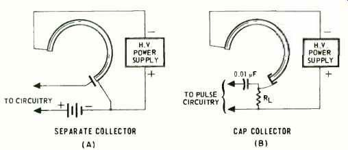
Fig. 3. A separate or cap collector may be used in the "C "shaped
CEM. High voltage required is 2 to 4 kV.
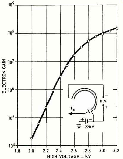
Fig 4. Electron-gain curve for Model CEM-4010 Channeltron.
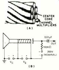
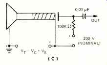
Fig. 5. (A) Basic Spiraltron configuration. (B), (C) Some typical circuit
arrangements for Model 4219X Spiraltron.
Spiraling the Channels
It was also found that ion feedback in the CEM could be suppressed by spiraling several channels around a central core. See Fig. 5A. This provided for more flexible configurations of these spiral OEM's, called Spiraltrons (SEM's) by Bendix. The straight cylindrical geometry of the Spiraltron allows it to be stacked into large matrices. In addition to being able to count single electron events, such matrices can also provide spatial information about the radiation source.
The Model 5205X Spiraltron bundle detector, for example, is a matrix (0.18 by 0.18-inch square) of Spiraltron electron multipliers. It is an area-sensitive detector for charged particles, energetic ultraviolet or soft x radiation, or metastable neutral particles. Each element of the matrix is capable of producing a pulse of 5 X 10' electrons for each detected input of electron, ion, or photon.
The location within the matrix of an output pulse can be determined to a resolution of 0.006 inch by using a movable anode or an array of discrete anodes. Additionally, the pulses at each output can be readily counted. The location of such pulses within the matrix can also be readily determined by accelerating the output charge pulses onto a phosphor screen.
Applications for this device include space experiment detectors, mass spectrometer detectors, line-array outputs for electron and ion energy analyzers, line-array outputs for vacuum ultraviolet spectrometers and soft x-ray spectrometers, mapping of weak ion and electron beams, and detecting charged particles and photons. The unit may be operated in either the pulse mode for detecting and counting or in the analog mode as a miniature area detector.
The Spiraltron may also be used as a single electron-multiplier element such as the Model 4219X. This model is made up of a flared (or funnel-shaped) input section, a straight channel preamplifier section, and a section containing six smaller spiral-wound channels. This configuration can be operated at high gains without ion feedback.
The Model 4219X can be operated in two basic circuit configurations as shown in Figs. 5B and 5C. As in the Channeltron circuits, the collector is spaced about 1 millimeter from the end of the unit and uses a nominal collector voltage of 200 volts. The three-terminal connection results in a slightly higher gain when a Vc of 500 volts is used. However, as noted in Fig. 6, values of Vc above and below 500 volts result in gains less than those obtained with the two terminal circuit configuration. Bendix does not recommend the use of a cap collector unless the cap is installed at the factory.
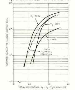
Fig. 6. Gain characteristic curves for the Model 4219X Spiraltron.