(source: Electronics World, Dec. 1971)
By KIRK BUTLER
Basic operation and specifications of these voltage-regulating diodes along with a simple design technique for using them as shunt regulators.
BEFORE one can design a voltage regulator, he must understand the characteristics of the regulating device, in this case the zener diode. Zener diodes are also known as avalanche or breakdown diodes. They are a special type of silicon junction diode and have characteristics very similar to those of ordinary silicon diodes. They conduct current very well when they are forward-biased, but become very poor conductors when reverse-biased.
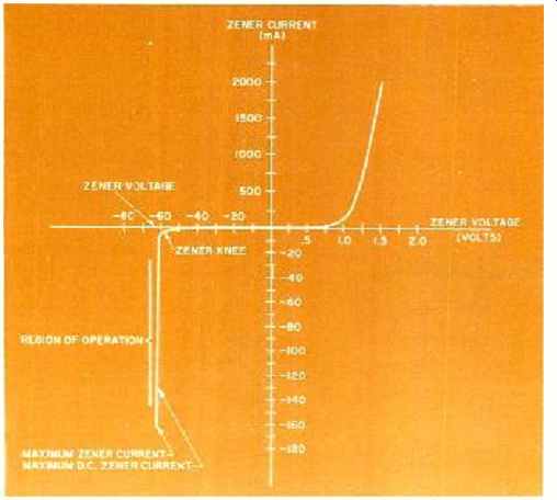
Fig. 1. Example of a zoner diode characteristic curve (1N3000).
When reverse-bias voltage across an ordinary silicon diode exceeds the peak reverse voltage (p.r.v.) rating of the diode, the diode will break down. When this happens to the ordinary silicon diode, it conducts excessive reverse current and the diode is usually destroyed. The zener diode, however, is designed to operate in this breakdown region.
The characteristics of a zener diode can be seen in Fig.1.
On the plot, negative voltages and currents represent reverse bias. From Fig. 1 it can be seen that the diode passes very little current when it is reverse-biased below the breakdown point. However, when the reverse-bias voltage reaches the breakdown point, the diode starts to draw current. Beyond this point, current will increase rapidly but voltage will remain almost constant. The point where the reverse current starts to increase rapidly is called the "zener knee." The zener diode is useful as a voltage regulator when it is operated between the zener knee and the maximum allowable reverse current.
The Zener Diode
Every zener diode has a set of specifications which describe its electrical, physical, and thermal properties. These specifications are available in manufacturers' publications, including catalogues, brochures, data sheets, application notes, and handbooks. Obviously, the zener-diode specifications must be known before a voltage-regulator circuit can be designed. Refer to Glossary of Specifications.
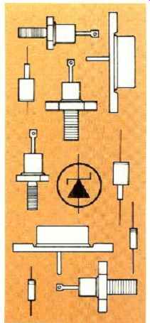
Zener diodes come in many different sizes, shapes, and cases. Fig. 2 shows some of the common shapes that zener diodes take and the diode polarity. Small diodes with axial leads usually have a ring on the cathode end. One- and ten-watt diodes quite often have the schematic symbol printed on the diode to indicate polarity. Ten-watt stud mounted zeners are available with standard anode-to-case polarity, or can be ordered with reverse polarity (cathode to case). Fifty-watt zener diodes are available in a TO-3 case or in a stud configuration, both in standard (anode-to-case) and reverse polarities.
The mounting of zener diodes is important not only to secure the diode, but also to dissipate heat.
When mounting axial-lead zeners, one should keep lead lengths as short as possible. This enables much of the heat dissipated by the diode to flow out the leads, since metal leads conduct heat much better than the surrounding air.
Thermal resistance of a typical axial-lead zener diode is three times greater with 7/8-in leads than with 'Is-in leads.
The mounting of high-power zener diodes in TO-3 or stud cases is even more important. These diodes must be mounted on a chassis or heat sink in order to dissipate the heat properly.
Heat is best transferred from the zener diode case to the heat sink when the zener is simply bolted to the heat sink.
This makes a metal-on-metal contact between diode and heat sink and provides excellent heat transfer. This arrangement, however, also connects the diode case to the chassis or heat sink electrically. Since the diode must often be electrically insulated from the chassis, mounting kits which include insulating spacers and washers are available for 10and 50-watt zener diodes. Fig. 3 shows typical mounting of power zener diodes.
A measure of how much a zener diode junction heats up for each watt of power dissipated is the junction-to-case thermal resistance. For heat-sink-mounted diodes, this is the thermal resistance mentioned in the glossary of zener specifications. Case-to-heat-sink thermal resistance depends on the way in which the diode is mounted. It is also measured as temperature rise per watt of power dissipation. This thermal resistance can often be reduced by sealing the diode with a compound after it is mounted. Data which gives the actual case-to-heat-sink thermal resistance for various mounting configurations is generally found along with mounting information. There is also a heat-sink-to-ambient thermal resistance which is a measure of how well the heat sink dissipates heat into the surrounding air.
This thermal resistance is also measured in temperature increase per watt of power dissipation of the diode mounted on the heat sink. Values of heat-sink-to-ambient thermal resistance are available from the heat-sink manufacturer or in many catalogues.
Thus an axial-lead zener diode has only one thermal resistance rating, whereas a chassis or heat-sink-mounted diode has three thermal resistance ratings. These thermal resistances will be used in the design procedure in order to calculate maximum diode temperature.
========================
GLOSSARY OF SPECIFICATIONS
Zener Power Rating: This is the maximum power, in watts, which the zener-diode junction is capable of dissipating. Some common zener power ratings are '/a W, '/z W, 1 W, 10 W, and 50 W.
Zener Voltage: The reverse-bias voltage at which breakdown occurs is called the zener voltage, the breakdown voltage, or the nominal zener voltage. Zener diodes are available with zener voltages ranging from several volts to several hundred volts.
Zener Tolerance: The tolerance of a zener diode is a tolerance on the rated zener voltage. Common tolerances are ±20 %, ±10 %, and ±5% although closer tolerances are available.
Maximum D.C. Zener Current: This is the maximum continuous or direct current which the diode can safely handle for thermal reasons. Currents in excess of the maximum d.c. zener current can be handled for short periods of time, or periodically, but not continuously. The maximum d.c. zener current is less than the maximum allowable zener current, which can be obtained by dividing the zener power rating by the zener voltage.
Zener Knee Current: This is the reverse current which flows through the zener diode at the breakdown point or zener knee. Knee currents range from 0.25 mA to 5 mA
Maximum Junction Temperature: To remain reliable, the junction of any solid-state device cannot exceed a given temperature in storage or in use. Maximum zener-diode junction temperatures are typically 175° or 200 °C. Since heat is generated in the junction and dissipated by the case, the case is cooler than the junction. Junction temperature cannot be measured directly, but must be calculated.
Thermal Resistance: Power dissipated in a zener-diode junction causes the diode to heat up. The thermal resistance relates junction temperature increase above the surrounding temperature to diode power dissipation which causes it. Thermal resistance is specified as the number of degrees of junction temperature increase per watt of junction power dissipation. Typical values of thermal resistance range from 1°C per watt for large diodes on heat sinks to 250 °C per watt for small diodes with axial leads.
Power-Derating Factor: When the ambient or surrounding temperature is high, the temperature increase from power dissipation can cause excessive junction temperature. For this and other reasons, maximum power which a diode can handle becomes less as the ambient temperature increases. Most diodes are rated for full-power operation with a surrounding temperature of 25 °C, approximately room temperature. If the actual ambient temperature is above 25 °C, zener power capacity is reduced by a derating factor, a given amount for each degree above 25 °C. Typical derating factors go from 0.001 watt per °C to 0.5 watt per °C, for temperatures above 25 °C. Some diodes must be derated above temperatures other than 25 °C. This figure would be included in manufacturers' specifications if it were any temperature other than 25 °C.
Zener-Voltage Temperature Coefficient: As temperature increases, the zener voltage changes. The temperature coefficient is usually given as a percentage change in zener voltage per 1 °C temperature rise. Typical voltage temperature coefficients range from -0.05% per °C to +0.15% per °C. A positive temperature coefficient indicates that zener voltage increases as temperature rises, while a negative temperature coefficient indicates that zener voltage decreases as the temperature rises.
========================
Shunt-Type Zener Diode Voltage Regulator
Although there are many uses for zener diodes, the most common is the shunt-type zener diode voltage regulator. It is a simple, economical, and reliable method of d.c. voltage regulation.
The schematic of a voltage regulator is shown in Fig. 4.
The power source might be a battery, generator, or an unregulated power supply. The load is the electronic device or circuit which requires a regulated voltage. The regulator consists of only two components, a resistor and a reverse-biased zener diode (the anode is connected to the negative side of the power source). The purpose of the regulator is to provide a constant voltage for the load, irrespective of variations in load current, power-source voltage, or any other factor.
It can be seen from Fig. 4 that both load and zener current must pass through R1, the resistor in the regulator circuit. The current through this resistance will cause a voltage drop across it. This means that the power-source voltage must always be higher than the regulated load voltage, since there is a voltage loss in the regulator itself.
Ohm's law tells us that the voltage drop across R1 is proportional to the current through it.
In the design process, the value of resistor R1 is made small enough so that most of the source voltage is dropped across the parallel combination of the zener diode and load.
Since the diode and load are in parallel, the load voltage is the same as the reverse-bias zener voltage. Furthermore, this voltage is the reverse breakdown voltage of the zener diode. It can be seen from the zener characteristic curve that, if there is a minute increase in load voltage (or reverse-bias zener voltage), zener-diode current skyrockets.
This increased current flows through R1, thus increasing the voltage drop across R1 and counteracting the load-voltage increase. The zener diode cannot overcompensate since it stops drawing current if load voltage drops below the zener breakdown voltage. However, the zener will not under compensate either since the zener current goes way up if voltage across the reverse-biased zener rises only a minute amount.
Similarly, if the load voltage (or reverse-bias zener voltage) decreases slightly, the zener diode draws much less current and reduced current flow through R1 causes the resistor voltage to decrease and load voltage to increase.
It can be seen, therefore, that an equilibrium will result and the zener diode will compensate for load-voltage variations and cause the load voltage to be almost perfectly constant, at the zener voltage. The zener diode only does this, however, if it is operated in the breakdown region of the curve. The object of voltage-regulator design is to select the proper component values so that the zener diode operates only in the breakdown region, thereby assuring regulation.
In a d.c. voltage regulator, the zener diode is always reverse-biased. Therefore, only the reverse-bias portion of the characteristic curve is considered in the design and whenever zener current is referred to, one can assume that this is a reverse current.
Design of Shunt-Type Regulator
The object of the design procedure is to determine the value of the two regulator components, R1 and the zener diode. Load-current variations, unregulated source-voltage variations, and the ambient temperature must be known in order to complete the design. It is necessary to deal with some thermal factors in the design of a voltage regulator, since they can be the most restricting factors.
The first step is to select the zener voltage. It will be the same as the regulated-load voltage, since they are in parallel. Therefore, the particular zener diode which will later be selected for the circuit must have a zener voltage equal to the desired regulated-load voltage.
Tolerance on the load voltage must also be considered. If the zener tolerance is equal to or less than the tolerance on the load voltage, the regulated voltage will be within the required limits. Actual zener voltage is not exactly the voltage which the manufacturer specifies but is within a given tolerance of the voltage specified.
Before designing a regulator it is necessary to know how the load current will vary. One must determine what the minimum and maximum load currents will be. Minimum load current may be zero for some loads if they sometimes become an open circuit. It may be possible to measure load current directly.
If it is not convenient to measure minimum and maximum load current, and they cannot be easily calculated, it may be necessary to estimate them in order to carry out the design. If this is done, the maximum possible load current should be estimated high and minimum load current low in order to assure that the regulator is designed to handle any load-current variation which it will encounter.
Input to the regulator circuits is, of course, an unregulated power source. Since it is unregulated, source voltage will vary between some minimum and maximum value. It is necessary to know the minimum and maximum value of the source voltage in order to carry out the regulator design. It is important to remember that in order for the regulator to function, the minimum source voltage must be greater than the zener voltage.
When the circuit is designed, two primary factors which vary and must be considered are the load current and the unregulated source voltage. As these factors vary, zener current will vary in order to maintain regulation. However, to maintain regulation, the zener must always operate in the breakdown region. This means that zener current must always be greater than zener knee current. However, the exact zener knee current is unknown since the power rating of the zener diode is not known. Thus the design is carried out under the assumption that zener current should never drop below a value which is arbitrarily set at one tenth the maximum load current. This assumption is checked following the design of the regulator circuit.
Zener current reaches a minimum value when the source voltage is minimum and load current is maximum.
Therefore, under these two conditions for minimum zener current flow, zener current must be equal to or greater than one tenth the maximum load current.
This dictates the value of R1. Voltage across R1, under these conditions, is equal to the minimum source voltage minus the zener voltage. Current through R1 is equal to the minimum zener current plus the maximum load current. After calculating voltage across R1 and current through it, the value of R1 is calculated by Ohm's law. The value of R1 must not exceed this calculated value in order to assure that the zener diode always draws sufficient current and remains in the breakdown region.
The power rating of R1 is easy to determine. Since the zener voltage remains constant, any variations in the source voltage will appear across R1. The voltage across R1 and power dissipated in it will be maximum when the source voltage is maximum. This maximum voltage across R1 is equal to the maximum source voltage minus the zener voltage. Maximum current through R1 is equal to the maximum voltage across R1 divided by its resistance. The maximum power dissipated in R1 is the product of maximum voltage and maximum current so R1 must be capable of handling this maximum power.
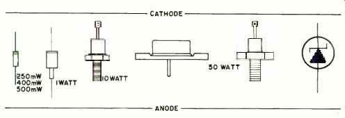
Fig. 2. Physical characteristics (and symbol) of some zener diodes. Standard
polarity is with anode connected to case.
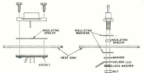
Fig. 3. Typical mounting arrangements for power zener diodes.
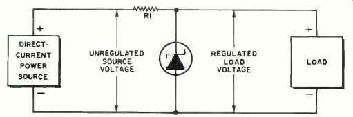
Fig. 4. Schematic of shunt-type zener diode voltage regulator.
The zener-diode power rating must also be determined.
Since power is the product of 'voltage and current and the zener voltage is constant, the necessary zener power depends on the maximum current the zener diode will draw.
Current through R1 splits and goes through the zener diode and the load. The maximum-current through R1 was previously calculated and the minimum load current must be known, as was mentioned previously. Maximum zener current is maximum current through R1 minus the minimum load current. The power rating of the zener diode must be selected so that its maximum d.c. zener current rating is greater than the maximum current to which the diode will be subjected in the circuit.
However, since a diode is not capable of dissipating as much power at high ambient temperatures as it can at low temperatures, the power-derating factor must be considered. The temperature above which a diode must be derated, and the derating factor, are given in the manufacturer's specifications for the selected diode. The power-derating factor must be multiplied by the maximum number of degrees by which the actual ambient temperature will exceed 25 °C (or a different temperature, if the manufacturer so specifies). This gives the number of watts by which the diode must be derated. This figure is then subtracted from the diode power rating to give maximum diode power dissipation at the ambient temperature.
The voltage-regulator design must now be checked to assure that the diode power dissipation does not exceed this new restriction. The maximum power which will actually be dissipated by the diode in the designed circuit is equal to the zener voltage times maximum current flow through the zener, as previously calculated. If the power dissipated by the diode in the circuit will exceed the derated power rating of the selected diode, a zener diode with a higher power rating must be chosen.
In the above design, several things were ignored or assumed. These factors should now be checked before the regulator is assembled.
First, in calculating R1 it was necessary to assume that the zener knee current is less than one tenth the maximum load current. Now that the zener diode has been selected, and the zener knee current determined from a data sheet on the diode, this assumption should be checked. If the zener knee current turns out to be greater than one tenth the maximum load current, the value of R1, the R1 power rating, and zener power rating must be recalculated using the zener knee current as the minimum. This is not often necessary.
Another thermal factor must also be taken into account.
The zener voltage of a zener diode does not always remain perfectly constant as we have thus far assumed. Unfortunately, zener voltage varies with temperature for most types. When a zener diode gets hot, the zener voltage may increase or decrease depending on its temperature coefficient, as discussed earlier. These variations are usually small and unimportant, but in some cases when the diode gets quite hot, it can make a difference.
It is first necessary to calculate the maximum temperature the zener diode will reach. The increase above ambient is found by multiplying maximum power dissipation (calculated) by the thermal resistance of the diode (from manufacturers' specifications). For a heat-sink-mounted zener, maximum power dissipation must be multiplied by the sum of the three thermal resistances in order to get the maximum temperature increase above ambient.
The maximum temperature the zener diode will reach is now calculated as the sum of the ambient temperature and the temperature increase due to power dissipation.
Now that maximum zener temperature is known, "worst case" zener voltage drift which is caused by temperature can be calculated. The amount by which the maximum zener temperature exceeds 25 °C is multiplied by the zener voltage temperature coefficient to yield the "worst-case" percent change in zener voltage due to temperature.
Of course, any change in zener voltage is a change in load voltage, so this result should be compared to the design requirements to determine if the particular design is satisfactory.