Use of the field-effect transistor presents few problems in conventional receiver circuits. In fact, some high-voltage FET's, such as Crystalonics Type C632, will replace tubes directly at the original plate voltages if cathode resistors are changed ( where this is required) and i-f and r-f stages are neutralized when these stages oscillate with triodes. Lower-voltage FET's may be employed readily in receiver circuits set up especially for their use.
The receiver circuits given in this Section are of especial interest to the hobbyist and experimenter. In addition to actual receivers, some accessory devices for use with receivers are also described.
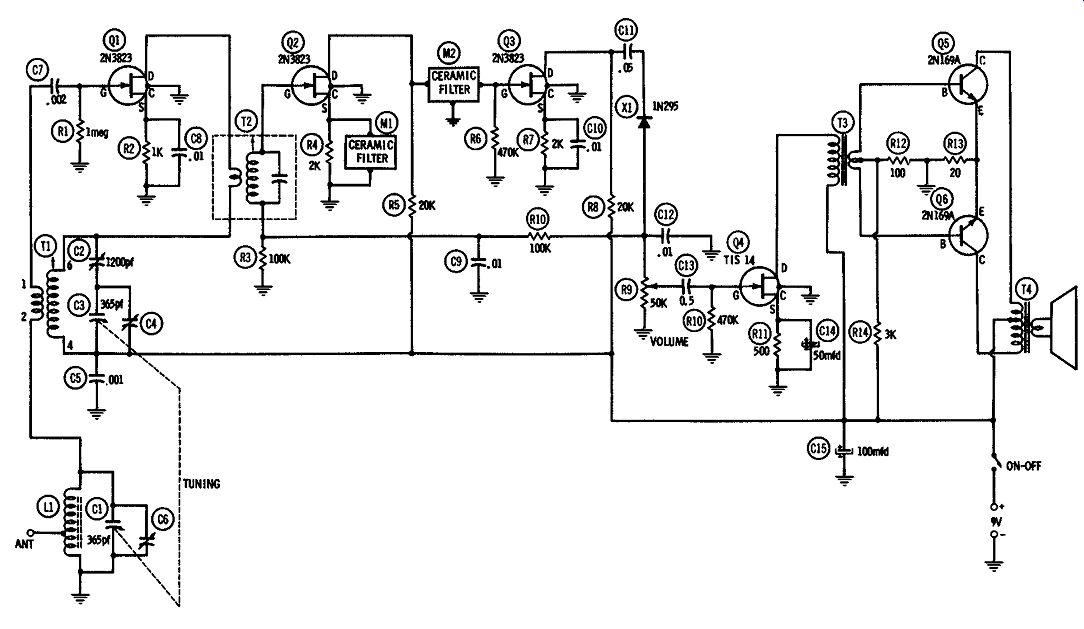
Fig. 1
SUPERHET BROADCAST RECEIVER
Fig. 1 shows the circuit of a superheterodyne broadcast-band receiver (540-1650 kHz). Three 2N3823 FET's are employed in the combined oscillator-converter ( Q1) and first and second r-f amplifiers ( Q2, Q3); a TIS14 FET ( Q4) is used in the a-f driver stage.
The second detector is a 1N295 ( X1), and the push-pull, class-B a-f output stage employs 2N169A bipolar transistors ( Q5, Q6).
The self-contained ferrite antenna, L1, is a Miller 2004 ( or equivalent). Because the FET produces negligible loading, Q 1 is connected across this entire antenna coil, and an outside antenna (when used) is connected to the low-impedance tap (ANT), giving a signal step-up through the autotransformer thus created. The oscillator transformer, T1, is a Miller 2020 transistor-type unit ( or equivalent). Tuning throughout the standard-broadcast band is accomplished with dual 365-pf variable capacitor C1-C3. Trimmer capacitors C4 and C6 are part of the tuning capacitor, but C2 is a separate padder with 1200-pf maximum capacitance. During initial alignment of the receiver, the antenna and oscillator are trimmed by means of C6 and C4, respectively, and the oscillator adjusted additionally with the aid of the tuning slug of TL. The converter is coupled to the i-f amplifier through a conventional transistor-type i-f transformer, T2, which is reverse connected, as shown. The i-f amplifier is fixed-tuned and needs no alignment adjustments. The self-tuning of the circuit to 455 kHz is provided by a Clevite TF-OlA ceramic filter ( M1) which replaces the bypass capacitor across source resistor R4, and by a U. S. Sonics A25H4C ceramic filter ( M2) inserted between the two i-f stages.
The 1N295 diode, X1, is a combined second detector and age rectifier. The volume-control potentiometer ( R9) serves the additional function of d-c load resistor for this diode, and the age voltage is taken from the top of the potentiometer and fed back to the first i-f stage through filter C9- R10. The audio component of the detector output is taken from the potentiometer through coupling capacitor Cl3 and is presented to the gate of the FET driver (Q4). The class-B coupling transformers are miniature transistor type units: Input transformer T3 (Allied Radio 54-D-2389, or equivalent) has a 10K primary and 3K center-tapped secondary; output transformer T4 (Allied Radio 54-D-2358, or equivalent) has a 500-ohm center-tapped primary and a 4-ohm secondary.
The receiver delivers audio-output power of approximately 110 milliwatts to the speaker. With a d-c supply of 9 volts, the current drain is 11 ma at zero signal; the drain is 260 ma when a maximum signal is received.
All fixed resistors are 1/2 watt, and electrolytic capacitors Cl4 and Cl5 are rated at 25 dcwv. Each FET has a fourth pigtail which is connected to the metal shell internally and must be grounded as shown.
REGENERATIVE BROADCAST RECEIVER
The regenerative broadcast-band receiver circuit shown in Fig. 2 will interest experimenters and hobbyists. This circuit, employing one 2N3578 FET, makes a sensitive receiver which is surprisingly selective for a regenerative setup. It picks up local stations with a self-contained ferrite loop antenna, L1, and can bring in weak and distant stations with an outside antenna and ground.
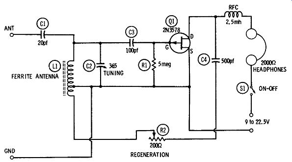
Fig. 2. Regenerative broadcast receiver.
The 365-pf variable capacitor, C2, tunes the loop antenna through out the standard-broadcast band ( 540-1650 kHz), and the 200-ohm rheostat, R2, provides smooth control of regeneration from zero to full oscillation. Very strong stations come in satisfactorily with no regeneration at all ( i.e., with R2 set to its maximum resistance), whereas weak stations are missing unless a good deal of regeneration is used. When the listener is hunting for a very weak station, he can use maximum regeneration, which will produce a whistle when the station carrier is located. He then can reduce the regeneration to the point at which the whistle just disappears.
The circuit operates at battery voltages between 9 volts and 22.5 volts, the higher voltages giving highest sensitivity and loudest signals. With 2000-ohm headphones in the circuit, the current drain is 3 ma at 9 volts, and 4 ma at 22.5 volts.
For increased volume, as for speaker operation, a suitable transistorized audio amplifier may be added to the receiver through a coupling transformer substituted for the headphones.
ALL-WAVE REGENERATIVE RECEIVER
The simplest possible sensitive receiver for all-wave general coverage and amateur-band phone and c-w reception is the regenerative type. Fig. 3A shows the circuit of a receiver of this kind which tunes from 3.5 to 35 MHz with five plug-in coils.
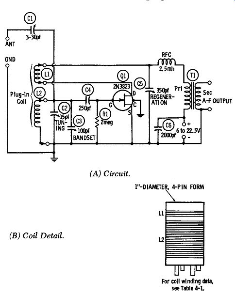
Fig. 3. All-wave regenerative receiver. (A) Circuit. (B) Coil Detail.
A simple detector with drain tickler feedback is employed. L1 is the tickler coil, and L2 the tuning coil. Both coils are wound on a I-inch-diameter, 4-pin, plug-in form, as shown in Fig. 3B. Variable bypass capacitor C5 is the regeneration control and is a midget 350-pf single-section unit. Audio output is delivered by T1, which may be any convenient transistor- or tube-type interstage trans former with a step-up turns ratio. Either headphones or an a-f amplifier may be operated at the A-F OUTPUT terminals.
The d-c operating voltage may be any available value between 6 and 22.5 volts, the higher values giving best sensitivity and loudest signals. The current drain is 4 ma at 6 vdc, and 8 ma at 22.5 vdc.
Table 1 gives coil-winding data. Some experimentation with the number of turns shown in this table may be necessary, since the FET and circuit capacitances will vary in individual layouts and will alter tuning characteristics. Coils LI and L2 must be wound in the same direction. The coils may be plugged into a standard tube socket.
If the receiver is used for ham-band reception, C3 will be used to set the receiver to the top of the band ( with C2 set to zero capacitance) and bandspread tuning will be afforded by C2. For general-coverage tuning, C2 must be set to minimum (zero) capacitance and the receiver tuned by means of C3. Antenna trimmer C1 must be adjusted for minimum detuning by the outside antenna used.
----------------

Table 1. Coil Winding Data for All-Wave Regenerative Receiver"'
80-METER BAND (3.5-4 MHz)
20 turns No. 30 enameled wire, close-wound immediately at top of L2 50 turns No. 24 enameled wire, close-wound 40-METER BAND (7-7.3 MHz)
8 turns No. 30 enameled wire, close-wound 1/8 inch from top of L2 17 turns No. 22 enameled wire, spaced to winding length of 3/4 inch 20-METER BAND (14-14.35 MHz)
6 turns No. 22 enameled wire, closewound 1/4 inch from top of L2 10 turns No. 22 enameled wire, spaced to winding length of 3/4 inch 15-METER BAND (21-21.45 MHz)
L1: 4 turns No. 22 enameled wire, closewound 1/4 inch from top of L2 L2: 7 turns No. 22 enameled wire, spaced to winding length of 3/4 inch IO-METER BAND (28-29.7 MHz)
L1: 3 turns No. 22 enameled wire, closewound 1/4 inch from top of L2 L2: 4 turns No. 22 enameled wire, spaced to winding length of 3/4 inch
__All coils wound on 1-inch diameter, 4-pin coil forms (Millen 45004 or equivalent). See Fig. 3(B).
----------------------------------
SINGLE-FREQUENCY, CRYSTAL-CONTROLLED CONVERTER
Fig. 4 shows the circuit of a crystal-controlled superhet converter which may be used ahead of an available i-f amplifier/detector/a-£ amplifier channel. This arrangement is based on 2N3823 FET' s as mixer ( Q 1) and oscillator ( Q2). This arrangement is intended for highly stable single-frequency reception, such as the monitoring of one station in standby service for communication or control purposes.
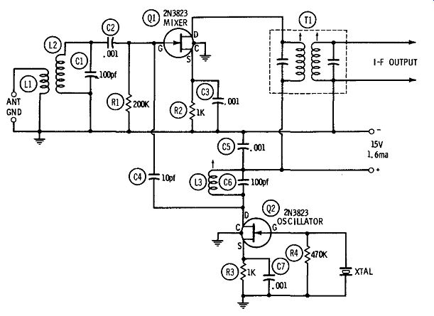
Fig. 4. Crystal-controlled converter.
The antenna input coupler is composed of coils L1 and L2, and tuning capacitor C1. The inductance of L2 is selected such that the desired signal frequency (f s) can be reached by varying C1, and the frequency ( f x) of the crystal ( XT AL) is chosen lower than the signal frequency by the amount of the intermediate frequency (flf ), i.e., fx = fs - f;r- Similarly, i-f transformer T1 must be tunable to the desired intermediate frequency. The primary coil ( L1) of the antenna coupler will contain one-fourth to one-third the number of turns in the secondary coil ( L2). The oscillator is tuned to the crystal frequency by adjustment of coil L3.
As a design example, consider that the converter is to operate into a 455-kHz i-f channel and that the received signal will be 5 MHz.
( 1 ) The crystal frequency must be 5000 - 455 = 4545 kHz.
( 2) To tune to this frequency, with C6 = 100 pf, L3 must be adjustable to 12.2 µ,h, neglecting circuit and FET capacitances.
( 3)
For good leeway of adjustment, let the 5-MHz signal be tuned in with C1 set to half-range, i.e., to 50 pf. This will require that L2 be 20 µ,h, neglecting circuit and FET capacitances. This value of inductance is obtainable in commercial slug-tuned coils to which a primary ( L1) may easily be added by winding insulated wire around the bottom of the coil. Alternatively, a 20-µ,h coil system may be wound on a I-inch-diameter form, with L2 = 6 turns of No. 22 enameled wire spaced to a winding length of 1/2 inch, and L1 = 3 turns of No. 22 enameled wire closewound 1/8 inch from the bottom of L2.
For stability, all wiring must be as short, rigid, and direct as practicable. A fourth pigtail of the 2N3823 is internally connected to the metal case of this FET, and for shielding purposes should be grounded as shown. All resistors are 1/2 watt; and for maximum stability, all capacitors should be silvered mica.
At 15 vdc, the total current drain is 1.6 ma.
BEAT-FREQUENCY OSCILLATOR
In a standard superhet receiver, a beat-frequency oscillator ( bfo) is needed for c-w reception. The usual procedure is to operate the bfo at the intermediate frequency and to couple its output into the second detector. A slight detuning of the bfo then will cause a beat note with the i-f carrier and will make the c-w signal audible. Fig. 5 shows the circuit of a bfo, using a Ul83 FET, which may be used with a receiver having no bfo of its own.
This Colpitts-type circuit operates at 455 kHz, the oscillation frequency being determined by 2.5-mh inductor L1 (which may be a conventional r-f choke of that inductance) and the series-parallel arrangement of capacitors C1, C2, and C3. The frequency is set initially, with C3 set to mid-capacitance, by adjustment of the tuning slug in coil L1 ( Miller 21A223RBI, or equivalent). Subsequent tuning of variable capacitor C3 adjusts the pitch of the beat note to suit the operator's ear.
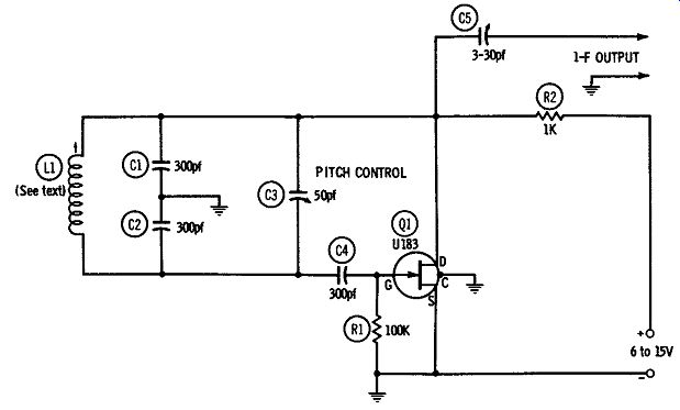
Fig. 5. Beat-frequency oscillator.
At 6 vdc, the current drain is 2 ma and the no-load i-f output is 5 volts peak to peak; at 9 vdc, the current drain is 2.1 ma and the i-f output 7 volts peak to peak; and at 15 vdc, the current drain is 2.2 ma and the i-f output 8.5 volts peak to peak. The bfo output is coupled to the second detector in the receiver through a 3-30-pf trimmer capacitor, C5. This capacitor must be set for optimum signal for a smooth beat note without receiver blocking.
Resistors R1 and R2 are 1/2 watt, and capacitors C1 and C2 are silvered mica. For stability, all wiring must be kept short, rigid, and direct, and the fourth pigtail of the Ul83 ( which is internally connected to the metal case of this FET) should be grounded as shown.
The bfo may be adapted to a higher intermediate frequency by using a lower-inductance coil in place of the 2.5-mh unit shown in Fig. 5.
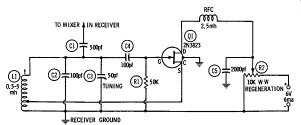
Fig. 6. Q-multiplier.
Q-MULTIPLIER
The Q-multiplier is a handy device for boosting the selectivity of a receiver in either phone or c-w reception. This device is especially valuable when the receiver has no crystal filter. Regeneration in the Q-multiplier sharpens the response of the i-f channel so as to peak a desired signal or reject an undesired one. Fig. 6 shows the circuit of a simple Q-multiplier employing a 2N3823 FET and designed for receivers having a 455-kHz i-f channel. The output of this instrument is coupled, through capacitor C1, to the plate, collector, or drain in the mixer stage of the receiver ( depending upon whether the receiver uses tubes, bipolar transistors, or field-effect transistors). The Q-multiplier shown here is a 455-kHz Hartley oscillator with controlled regeneration. The operating frequency is determined by coil L1 ( Miller 6323, or equivalent) which is adjustable between 0.5 and 5 mh, and capacitors C2 and C3. Initially, the instrument is set to 455 kHz, with C3 set to midcapacitance, by adjustment of the tuning slug in the coil. Capacitor C3 then is used subsequently to tune the multiplier sharply to the receiver intermediate frequency.
The amount of regeneration, and thus the selectivity of the receiver, is controlled by varying the FET d-c voltage with the 10,000-ohm potentiometer, R2. Two modes of operation are obtained: with a certain amount of regeneration, the Q-multiplier acts as a notch filter, eliminating a signal to which the receiver is tuned; with more regeneration, the i-f response is peaked, tuning the receiver sharply to one desired signal coming in on the set.
The shortest possible leads must be used between Q-multiplier and receiver. Also, all wiring inside the Q-multiplier must be short, rigid, and direct. Resistor R1 is 1/2 watt, and capacitors C1, C2, and C4 are silvered mica. The instrument should be shielded by en closing it in a metal box, and for additional shielding the fourth pigtail of the 2N3823 ( being connected internally to the metal case of this FET) must be grounded as shown.
At 6 vdc, the total current drain is 6 ma. The d-c operating power for the Q-multiplier may be obtained from a self-contained battery or from the receiver power supply.
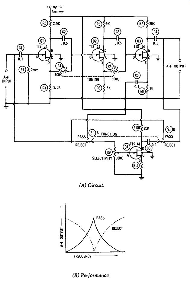
Fig. 7. "Selectoject." (A) Circuit. (B) Performance.
"SELECTOJECT"
The "Selectoject," like the Q-multiplier and the crystal filter, permits either the selection or rejection of a signal but on the basis of the latter's audio frequency. The "Selectoject" is connected between a-f stages of a receiver, or between second detector and audio channel.
Fig. 7A shows the circuit of a transistorized "Selectoject" employing four TIS14 FET's. Fig. 7B shows performance of the circuit. In this arrangement, which is essentially a sharply tuned a-f amplifier, a dual rheostat ( R4) serves as the tuning control. One rotation of this control tunes the "Selectoject" from 100 Hz to 10 kHz. Potentiometer R9 serves as the selectivity control ( for adjusting the sharpness of response to suit individual conditions) and dpdt switch S1 serves as the function switch ( for selecting either the pass or reject function of the circuit). With the function switch in its PASS position, the response at the frequency to which the "Selectoject" is tuned is shown by the solid curve in Fig. 7B. With this switch in its REJECT position, the response is shown by the dotted curve. The height of the pass curve or the depth of the reject curve, and the width of either curve, are controlled by the setting of potentiometer R9, highest selectivity in either case resulting when R9 is set for maximum gain in FET Q4.
The select/reject response of the circuit results from the fact that signal through the Q4 stage ( from input to output of the entire circuit) is negative when the function switch is thrown to REJECT and therefore cancels the tuned-in signal, whereas this feedback ( this time, from the source of FET Q3 to the input of the circuit) is positive when the function switch is thrown to PASS, and there fore boosts the tuned-in signal. If potentiometer R9 is advanced far enough when the function switch is set to PASS, the circuit will oscillate, delivering a sine-wave signal at the frequency to which tuning control R4 is set.
The resistance of R2 must be selected equal to the resistance of R3 within 1 percent. Similarly, the resistance of R5 must be selected equal to the resistance of R6 within 1 percent. Also, the capacitance of C2 must equal the capacitance of C3 within 1 percent. All fixed resistors are 1/2 watt.
For stability, all wiring must be kept as short, rigid, and direct as practicable. A metal case, to which the circuit is grounded, will shield the "Selectoject" from external fields, and for additional shielding the fourth pigtail of the TIS14 ( which is internally connected to the metal case of this FET) must be grounded as shown. Total current drain is 2 ma at 9 vdc.
AUDIO SQUELCH AMPLIFIER
Fig. 8 shows the circuit of a simple squelch amplifier which can hold the audio channel of a receiver silent until the receiver signal reaches a predetermined amplitude. This single amplifier stage may be inserted at any convenient point near the front end of the audio channel.
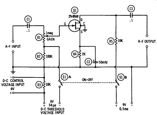
Fig. 8. Audio squelch amplifier.
The circuit is a simple r-c-coupled amplifier, based on a 2N4868 FET ( Q1), which is biased to cutoff by a d-c gate voltage applied to the THRESHOLD terminals. A d-c voltage, applied to the D-C CONTROL VOLTAGE terminals, bucks this bias and activates the amplifier whenever it exceeds the threshold cutoff voltage. The control voltage may be derived from the i-f amplifier (by rectification) or from the 2nd detector of the receiver. When the amplifier is in operation, it has a voltage gain of 10, with a maximum undistorted output of 1 volt rms. This means that the a-f input voltage at the gate of the 2N4868 must not exceed 0.1 volts rms for any setting of gain-control potentiometer R1.
Main current drain is 0.5 ma at 9 vdc. Virtually all of the current taken from the 6-volt threshold source flows through resistor R2 and is 54 microamperes. The d-c control voltage appears across resistor R3, and this creates a current of 0.6 ma through that resistor. While separate d-c voltage sources are shown for the main supply and the threshold, these voltages may be obtained from appropriate points in the receiver circuit (as along a voltage divider in the power supply.)
If a particular receiver circuit gives voltage of the polarity opposite to that shown in Fig. 8, use a P-channel FET ( such as 2N3578), change the values of R4 and R5 as required, and reverse capacitor C2.
Lead dress may be important in individual installations, so all leads must be kept as short and direct as practicable. Route them so as to avoid stray coupling in the receiver. A fourth pigtail of the 2N4868 is internally connected to the metal case of this FET and must be grounded as shown, for shielding. Resistors R2, R3, R4, and R5 are 1/2 watt. Capacitors C1 and C3 are 100-volt plastic units, and C2 is a 25-dcwv electrolytic.
[Note: This guide is based on Sams "FET Circuits", pub'd in 1961]