The sensitivity of the field-effect transistor to low signal levels and to small changes in level, together with its negligible loading of timing circuits, signal circuits, and actuating devices, suits it to a variety of electronic control circuitry where special provision often must be made for the bipolar transistor. Usually, a simple FET circuit in a control system offers straightforwardness and economy not so easily obtained with either tubes or bipolar transistors.
In solid-state control circuits, the FET allows some components, such as high-resistance photocells and capacitive transducers, to be operated with greater efficiency and convenience than is possible in such circuits containing bipolar transistors. And a special member of the field-effect family-the photo-FET, a light-sensitive FET-weds photocell and field-effect transistor.
This Section describes several basic control circuits which are intrinsically useful. Methods of operating relays from a variety of signals-direct current, radio frequencies, audio frequencies, and illumination levels-are shown. Perhaps these can also serve to generate ideas for other uses.
D-C RELAY
Fig. 1 shows the circuit of an amplifier-type d-c relay based on a single 2N3819 FET. This circuit has an input resistance of 10 megohms due entirely to resistor R1, so it draws only 0.15 microampere from the d-c control-signal source.
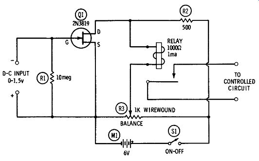
Fig. 1. DC relay.
The 1000-ohm, 1-ma d-c relay ( Sigma 5F, or equivalent) is connected in a resistance-bridge circuit whose four arms are R2, the internal drain-to-source resistance of the FET, and the two halves of potentiometer R3. With the DC INPUT terminals open, R3 is set to balance the static FET current out of the relay ( at balance, the relay opens firmly), and the bridge should remain balanced indefinitely without further attention.
Subsequent application of a d-c input signal of 1.5 volts will unbalance the bridge by changing the FET drain-to-source resistance; this will cause approximately 1.2 ma to flow through the relay, closing the latter. Up to 20 megohms may be used at R1, thereby decreasing the drain on the signal source to as little as 0.075 microampere.
All fixed resistors are 1/2 watt. Maximum current drain from the 6-volt d-c supply ( M1) is 10 ma. The 2N3819 is a plastic-encapsulated FET which, because of this construction, demands none of the installation precautions occasioned by metal-cased units. The plastic housing will withstand soldering temperatures.
AC R-F RELAY
The d-c relay described in the preceding section may be actuated by an AC or r-f control signal if a diode rectifier is operated ahead of the circuit, as shown in Fig. 2.
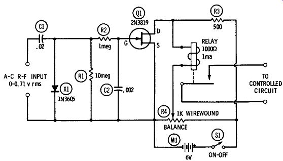
Fig. 2. AC r-f relay.
A shunt-diode rectifier circuit is used ( C1-· R1-X1 ). The main advantage of the shunt diode is isolation from any d-c component present in the signal source. In this arrangement, capacitor C1 is charged to the peak value of the a-c signal ( less the small forward voltage drop in the diode) on positive half-cycles of signal voltage, and this peak d-c voltage ( across 10-megohm load resistor R1) is presented to the gate of the FET. The diode must be polarized as shown for the d-c voltage at the gate to be negative. A silicon diode ( 1N3605) is required to work into the high load resistance, R1; the back resistance of germanium diodes is too low to support rectification with such a high value of load. Resistor R2 and capacitor C2 form a filter to remove any signal-voltage fluctuations from the diode d-c output.
The 1000-ohm, 1-ma DC relay ( Sigma 5F, or equivalent) is connected in a resistance-bridge circuit whose four arms are R3, the internal drain-to-source resistance of the FET ( 2N3819), and the two halves of potentiometer R4. With the AC-INPUT terminals open, R4 is set to balance the static FET current out of the relay ( at the balance point, the relay opens firmly), and the bridge should then remain balanced indefinitely without further attention.
Subsequent application of an a-c or r-f input signal of 0.71 volt rms will unbalance the bridge by changing the FET drain-to-source resistance, and this will cause approximately 1.2 ma to flow through the relay, closing the latter.
All fixed resistors are 1/2 watt, and capacitors C1 and C2 are mica. Maximum current drain from the 6-volt d-c supply ( M1) is 10 ma. The 2N3819 is a plastic-encapsulated FET which, because of this construction, demands none of the installation precautions occasioned by the metal-cased units.
The terminal arrangement of the FET's can be checked against the drawings shown in Appendix A. Manufacturers may be obtained from Appendix B, and the addresses are shown in Appendix C.
TOUCH-PLATE RELAY
The touch-plate relay has many commercial, industrial, and household applications. Touch the metal plate lightly and the relay closes; remove your finger and the relay opens. Call signals, safety devices, intrusion alarms, and kindred devices are operated from such relays.
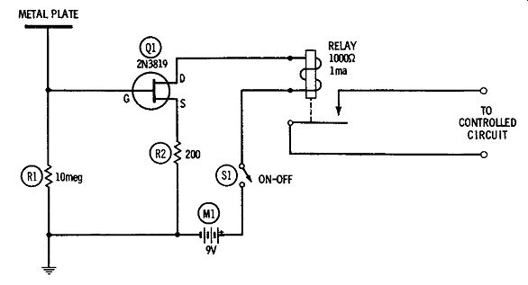
Fig. 3. Touch-plate relay.
Fig. 3 shows the circuit of a simple touch-plate relay based on a single 2N3819 FET. In this arrangement, the touch plate is a disc or plate of sheet metal or foil (2-inch minimum diameter) or a metal ball. When the plate is undisturbed, the FET draws negligible current through the relay ( Sigma 5F, 1000-ohm, 1-ma, or equivalent). When the plate is touched, enough stray noise is coupled into the 10-megohm gate circuit to boost the drain current to approximately 1.7 ma and close the relay. (This assumes a firm touch; a lighter touch will produce a lower current change, but the relay will close as long as this current reaches a minimum value of 1 ma.
If desired, a delayed dropout may be obtained by means of a capacitor in parallel with the relay coil. With the 1000-ohm coil, the hold-in is approximately 0.8 second per 1000 mfd of parallel capacitance.
Resistors R1 and R2 are 1/2 watt. The 2N3819 is a plastic encapsulated FET which demands none of the installation pre cautions occasioned by metal-cased units.
AMPLIFIED PHOTOCELL
The silicon solar cell ( self-generating type) is basically a low voltage, high-current device. In some applications, especially where high impedances are involved, more convenient control might be effected if the d-c output voltage of the cell could be boosted and the cell looked like a high-impedance source.
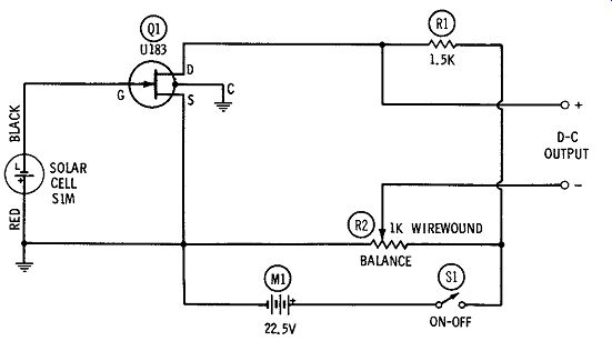
Fig. 4. Amplified photocell.
Fig. 4 shows the circuit of a simple d-c amplifier based on a single Ul83 FET. The maximum no-load output ( 0.4 volt) of the solar cell ( International Rectifier SIM, or equivalent) is amplified to 1.6 volts by this arrangement. A particular advantage of a circuit such as this is the high-resistance load which the FET input offers to the cell. On rapidly changing light signals and those modulated at high frequencies, this input avoids the high damping caused by the low resistances into which such silicon cells usually operate.
The output half of the circuit is a resistance bridge whose four arms are R1, the internal drain-to-source resistance of the FET, and the two halves of potentiometer R2. With the solar cell completely darkened, R2 is set to balance the static voltage from the D-C OUTPUT terminals ( a d-c vtvm temporarily connected to the output terminals will serve as a balance indicator). At the balance point, the indicator will read zero, and the bridge should then remain balanced indefinitely without further attention.
Subsequent illumination of the cell will unbalance the bridge because the DC output voltage of the cell changes the drain-to source resistance of the FET. This will cause 1.6 volts to appear at the D-C OUTPUT terminals. ( This level of output voltage will maintain itself across a 20,000-ohm load.) Wiring is uncritical. Resistor R1 is 1/2 watt, and potentiometer R2 is 1 watt. The fourth pigtail of the U183 is internally connected to the metal case of this FET and should be grounded as shown.
Total current drawn from the 22.5-volt source ( M1) is 24 ma.
PHOTO-FET RELAY
The photo-FET ( photoelectric field-effect transistor) has several advantages over photodiodes and bipolar phototransistors. It combines, for example, the functions of self-generating photo-junction and high-impedance-input amplifier. And it provides high amplification at low noise level ( 0.5-db typical noise). Fig. 5 shows the circuit of a light-sensitive relay employing a P-102 photo-FET. Note that this is a P-type field-effect transistor.
The P-102 has a built-in lens, which greatly simplifies application.
In this arrangement, the dark current in the photo-FET drain circuit is approximately 300 µa. When the FET is illuminated at only 10 foot-candles, the drain current increases to approximately 1.6 ma, more than enough to close the 2500-ohm, 1.4-ma DC relay ( Sigma 5F, or equivalent). If desired, a delayed dropout may be obtained by means of a capacitor in parallel with the relay coil. With the 2500-ohm coil shown, the hold-in is approximately 2.75 seconds per 1000 mfd of parallel capacitance. Current drain on the 1.5-volt gate-bias source, M1, is less than 0.1 microampere.
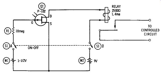
Fig. 5. Photo-FET relay.
Wiring is straightforward, and resistor R1 is 1/2 watt. The gate electrode of the P-102 is internally connected to the metal case of this FET, so the latter must be kept clear of contact with wiring, metal chassis, or other components.
TIMER
Resistance-capacitance-controlled timers have been built with vacuum tubes, thyratron tubes, bipolar transistors of all types, and with no tubes or other active devices whatever. The bipolar-transistor circuits, while offering the advantage of compactness, small size, light weight, freedom from the power line, and zero heat generation, have been troublesome to design because the low-impedance transistors load the r-c timing circuit and impose undesirable limitations on it. The high input impedance of the field-effect transistor, however, allows vacuum-tube performance to be attained in solid-state electronic timers.
Fig. 6 shows the circuit of a timer employing a single Ul83 FET. This is essentially a bridge-balanced d-c amplifier, with a relay in its output circuit, which receives its driving signal from a charged capacitor discharging through an adjustable resistor. It provides a hold-in of the relay that ranges from 1 second to 80 seconds, as selected by adjustment of the resistance.
The timing interval is determined by the number of seconds taken by 100-mfd capacitor C1, after being fully charged, to discharge through rheostat R1 to 0.4 of its charged voltage. This capacitor is charged by momentarily depressing push-button switch SL This connects C1 to a 1.5-volt tap on resistor R2. When released, the push-button blade returns to its normal position against the upper contact, and this connects the charged capacitor to rheostat R1 and the gate of the FET. The 1000-ohm, 1-ma d-c relay (Sigma 5F, or equivalent) is connected in a resistance bridge whose four arms are R3, the internal drain-to-source resistance of the FET, and the two halves of potentiometer R4. With capacitor C1 completely discharged, R4 is set to balance the static FET current out of the relay ( at balance, the relay opens firmly), and the bridge then should remain balanced indefinitely without further attention.
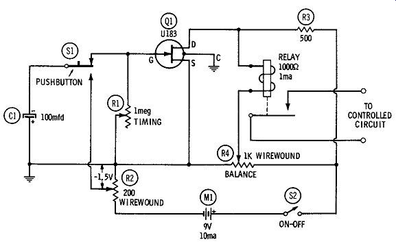
Fig. 6. Timer.
To use the timer, depress S1, charging capacitor C1. Then re lease this switch, whereupon the relay will pick up immediately, since the negative voltage presented to the FET gate by the charged capacitor unbalances the bridge, causing current through the relay. The relay will hold in until the capacitor has discharged sufficiently ( through rheostat R1) to reduce the gate voltage to 0.4 of its value at full charge of the capacitor. This time interval depends on the resistance setting of R1, and the rheostat accordingly may be calibrated to read directly in seconds. This may be done with a stopwatch, or the time ( t in seconds) may be calculated approximately from the resistance setting ( R1 in ohms), the capacitance ( C1 in farads), and a multiplier ( 0.8 for the relay specified here).
Thus: t = 0.0001 ( 0.8) R1 = 0.00008R1 (sec)
With a 1-megohm volume control having an audio taper for R1, time intervals from 1 to 80 seconds may be read on a single dial scale.
Various combinations of capacitance and variable resistance other than the 100 mfd and 1 megohm indicated in Fig. 6 may be used.
In any instance, the electrolytic capacitor used for the purpose should be new and have a good power factor. For close reading or for coverage of narrow bands, several switched-in rheostats may be used against a single capacitor.
Resistor RS is 1/2 watt; R2 and R4 may be wirewound rheostats with slotted shafts for screwdriver adjustment. Alternatively, R2 may be a stick-type resistor with slider. Electrolytic capacitor C1 is rated at 25 dcwv. The fourth pigtail of the Ul83 is internally connected to the metal case of this FET and should be grounded as shown.
FET AS VOLTAGE-VARIABLE RESISTOR
Since at any value of drain-to-source d-c voltage, the drain current is a function of the applied gate-to-source bias voltage, the instantaneous value of internal drain-to-source resistance depends on the d-c gate bias. This provides a convenient means of varying resistance with an available variable voltage; and since the correctly polarized gate bias in the FET results in virtually zero gate current, the process is essentially a voltage-controlled one.
Fig. 7A shows the simple setup of a U222 (high-current) FET as a voltage-controlled resistor. Here, the control voltage ( as gate bias) is applied to terminals A and B. Looking into terminals C and D, one see~ a resistor varied by the voltage on A and B. In use, this "resistor" is connected in series with a d-c supply and load device, the supply being polarized so that C is positive and D negative. Some devices in which a voltage-variable resistor is advantageous are voltage regulators, signal translators, voltage tuned frequency-sensitive RC networks, voltage-tuned audio oscillators, remote-control devices, temperature transducers, and remote volume controls.
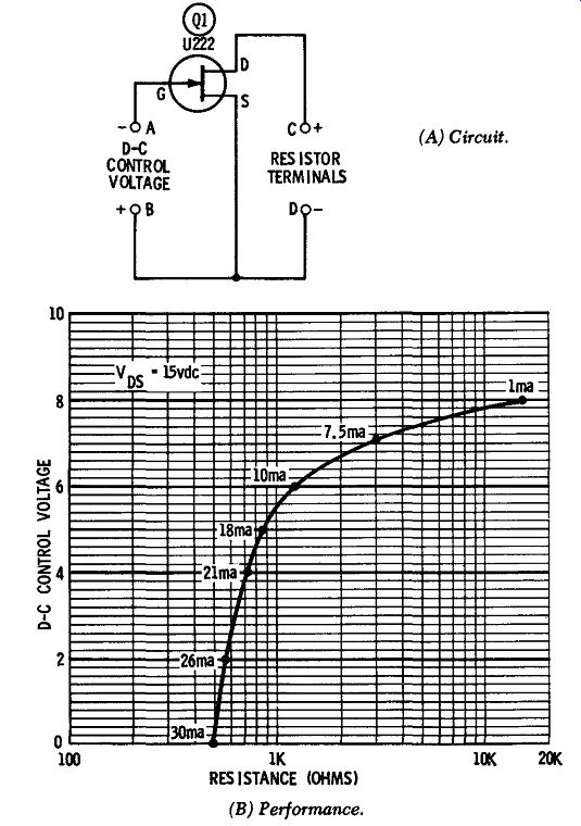
Fig. 7. FET 85 voltage-variable resistor.
Fig. 7B shows performance of the resistor when the voltage between C and D is 15 volts. Note that the resistance varies from 500 ohms ( when the control voltage is zero) to 15,000 ohms ( when the control voltage is - 8 volts). Other resistance ranges are obtained when the C-D voltage is some value other than 15 volts.
The power-handling capability of the variable FET resistor corresponds to the rated power dissipation of the FET. ( The manufacturer gives 300 mw as the absolute maximum device dissipation for the U222 at 25°C free-air temperature). Note that the corresponding drain-current values are given along the curve in Fig. 7B. When using any FET as a voltage-variable resistor, keep well within the maximum safe drain-to-source voltage, drain-current, and device-dissipation ratings supplied by the FET manufacturer.
The "resistor" may be calibrated by successively applying the various intended values of bias voltage and noting the corresponding drain current. The resistance is calculated at each point as VD/In, where VD is the instantaneous drain-to-source voltage ( in volts) and ID is the corresponding drain current (in amperes).
CONSTANT-CURRENT SOURCE
The pentode-like drain-voltage/drain-current characteristic curves of the FET suit this component for use as a constant-current adapter. Fig. 8 shows the circuit of such an adapter employing a TIX33 FET.
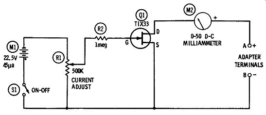
Fig. 8. Constant-current source.
The adapter is connected in series with an external d-c power supply and the device operated from the supply, with the supply polarized correctly to make terminal A of the adapter positive and B negative. Potentiometer R1 then is set for the desired load current, as indicated by 0-50 d-c milliammeter M2. ( With the TIX33, this may be any value between 1 and 40 ma.) That current level then will be maintained automatically within 6 percent, even if the voltage of the external supply varies between 3 and 20 volts.
Current drain from the 22.5-volt gate bias supply, M1, is 45 microamperes, which is due entirely to current through the 0.5 megohm potentiometer, R1. Resistor R2 is 1/2 watt.
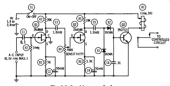
Fig. 9. Sensitive AC a-f relay.
SENSITIVE AC A-F RELAY
Using two FET's ( Q1, Q2) and one silicon bipolar transistor ( Q3), the circuit given in Fig. 9 closes a I-milliampere, 5-volt ( at approximately 0.1 microampere ), when gain control R4 is set to maximum. Good response is obtained throughout the spectrum from 50 Hz to 50 kHz.
The input signal is amplified by a two-stage r-c-coupled section based on two FET's: 2N4868 ( Q1) and 2N4340 (Q2). The amplified signal then is rectified by the 1N34A diodes ( X1, X2), and the resultant direct current is amplified by a 2N2712 plastic-encapsulated silicon bipolar transistor ( Q3) and applied to the 1-ma, 5000 ohm d-c relay ( K1, Sigma 5F, or equivalent). With zero input signal, the 2N2712 draws virtually no current, and the total circuit drain is 1.8 ma at 9 vdc. With a 0.1-volt input signal (R4 set for maximum gain), the circuit drain rises to 2.8 ma. d-c relay (K1) in response to an input signal of only 0.1 volt rms
All fixed resistors are 1/2 watt.
Capacitors C1, C3, C5, and C6 are 100-volt plastic units, and C2 and C4 are 25-dcwv electrolytics.
For stability, all wiring must be kept as short, direct, and rigid as practicable, and the entire unit should be enclosed in a grounded shield box if interfering fields are present. A fourth pigtail of the 2N4868 is internally connected to the metal shell of this FET and must be grounded as shown, for shielding. In the 2N4340, the gate electrode is internally connected to the metal case, so this FET must be mounted clear of chassis, wiring, and other components.
Signal input leads to the AC INPUT terminals should be shielded.
SOUND-OPERATED RELAY
Fig. 10 shows the circuit of a sound-operated relay based on two 2N4868 FETs ( Q1, Q2) and one 0183 FET (Q3). With this arrangement, a microphone output signal of 1.8 millivolts rms ( -52.5 db) will close the 1-ma, 1000-ohm d-c relay (K1) when sensitivity control R4 is set to maximum.
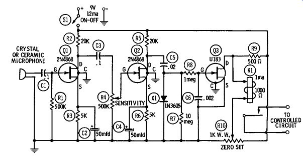
Fig. 10. Sound-operated relay.
The first two stages form a high-gain r-c-coupled amplifier, the output of which is rectified by the 1N3605 silicon diode, X1. The resultant d-c output voltage of the diode, developed across load resistor R7, is applied to the gate of the 0183 FET ( Q3) through the resistance-capacitance filter R8-C6. The 0183 acts as a d-c amplifier which drives a 1-ma, 1000-ohm d-c relay ( Sigma 5F, or equivalent). Current drain is 12 ma at 9 vdc.
Initial adjustment of the circuit consists of balancing the static drain current of the Ul83 out of the relay:
1. Short-circuit the microphone terminals.
2. Set potentiometer R4 for maximum sensitivity.
3. Adjust potentiometer R10 until relay K1 opens.
(This adjustment may be made very precisely if a d-c vtvm is connected across the relay coil and R1O is adjusted for zero deflection of the meter.) All fixed resistors are 1/2 watt. Potentiometer R10 is wirewound.
Capacitors C1, C3, C5, and C6 are 100-volt plastic units, and C2 and C4 are 25-dcwv electrolytics. The high-impedance input of the first stage will accommodate a crystal or ceramic microphone directly; for a dynamic microphone, use an appropriate input transformer.
For stability and minimum stray signal pickup, all wiring must be as short, direct, and rigid as practicable. For complete shielding in electrically noisy locations, the entire unit must be enclosed in a grounded metal box. In each of the FET's, a fourth pigtail is internally connected to the metal case and must be grounded as shown, for shielding.
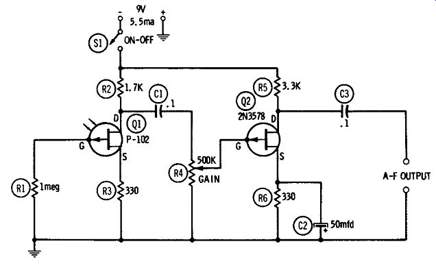
Fig. 11. Modulated light detector/amplifier.
MODULATED-LIGHT DETECTOR/ AMPLIFIER
The P-102 photo-FET is a good detector of modulated light ( either chopped or smoothly modulated), and its a-f output is easily amplified. Fig. 11 shows a circuit composed of a P-102 photo-FET ( Q1) and a 2N3578 P-channel FET (Q2) as an a-f amplifier.
The sensitivity of this circuit is such that 15 foot-candles of light modulated or chopped at a 1000-Hz rate will produce 1 volt rms (no load) at the A-F OUTPUT terminals when potentiometer R4 is set for maximum gain. Current drain is 5.5 ma at 9 vdc.
The detector/amplifier has many uses, such as light-beam communication, alarm signaling, intrusion alarm service, sound-on-film pickup, and optoelectronic control. The virtually zero loading of the photo-FET by the amplifier results in maximum efficiency of the P-102, while the amplifier produces a useful output-signal amplitude for direct application or further amplification.
All fixed resistors are 1/2 watt. Capacitors C1 and C3 are 100-volt plastic units, and C2 is a 25-dcwv electrolytic. In both the P-102 and the 2N3578, the gate electrode is internally connected to the metal case of the FET, so each of these units must be mounted clear of other components, chassis, and wiring. The P-102 must be positioned so that its nose-end lens faces the incoming light. All wiring must be as short, rigid, and direct as practicable.
PHASE SHIFTER
The circuit given in Fig. 12, combining a triode phase inverter and an adjustable r-c circuit, provides continuously variable phase shift from O to 180 degrees while leaving the signal amplitude virtually untouched.
This arrangement, based on one 2N3578 FET ( Q1), has equal fixed resistances ( R2 and R3, matched within 1 percent) in both drain and source legs. When rheostat R4 is set to one end of its range, the output is taken from the source of Q 1 and is in the same phase as the input signal (Q1 is then acting as a source follower); therefore, there is zero phase shift between output and input. But when R4 is set to the opposite end of its range, the output is taken from the drain of Q 1 and is of opposite phase from the input ( Q 1 then is acting as a conventional triode amplifier); therefore, there is then 180 degrees phase shift between output and input. At intermediate settings of R4, the various phase angles between 0 and 180 degrees are obtained. Two identical stages may be cascaded for 0 to 360 degrees phase shift.
The circuit provides good, full-range operation between 150 Hz and 5 kHz. Below 150 Hz and above 5 kHz, inherent phase shifts in the circuit and components restrict the range to limits somewhat higher than zero degrees on one end and somewhat lower than 180 degrees on the other. However, some improvement may be obtained by careful attention to lead dress and shortness of leads, and to minimizing stray capacitances.
For undistorted operation, the maximum input-signal amplitude is 2 volts rms. With potentiometer R1 set for maximum gain the corresponding output-signal amplitude is 0.75 volt rms. Current drain is 1 ma at 9 vdc.
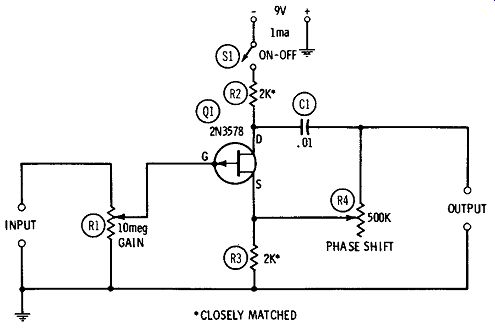
Fig. 12. Phase shifter.
Resistors R2 and R3 are 1 watt and are of the 1 percent non inductive, wirewound type. Capacitor C1 is silvered mica.
All wiring must be as short, rigid, and direct as practicable and kept well away from the metal chassis if one is used. The input and output circuits must be kept well separated. In the 2N3578, the gate electrode is internally connected to the metal case, so this FET must be mounted clear of other components, wiring, and chassis.
The dial of the phase-shift control, R4, may be calibrated in degrees by means of Lissajous figures. For this purpose, connect an audio-frequency signal generator to the INPUT terminals and to the vertical-amplifier input terminals of an oscilloscope having excellent phase characteristics, and connect the OUTPUT terminals of the phase shifter to the horizontal-amplifier input of the oscilloscope.
[Note: This guide is based on Sams "FET Circuits", pub'd in 1961]