VITAL to any circuit are the components or "hardware" that go into it. Printed-circuit components manufacture has taken many different paths. Some are merely those already developed for other purposes and are used without changes. Others have needed alteration for use with printed-circuit and subminiature assemblies. Still others have required entirely new development "from scratch." Many, such as wirewound pots and carbon resistors, are three-dimensional or "live" hardware. Printed and etched capacitors and resistors are essentially two-dimensional units, their thickness being negligible in most cases when compared to their other dimensions.
Many developments in subminiaturization and printed circuitry are awaiting the manufacture of certain components in particular forms. For instance, a two-dimensional variable resistor would open up new fields in printed-circuit packaging.
Even though a printed-circuit resistor ( fixed) is flat, the addition of a slider adds bulk and a third dimension. The most work to be done in printed circuits and subminiaturization lies in power sources. It is common to have a printed-circuit assembly which is one-third to one-fourth the size of the battery powering it.
Resistance components
The tape resistor, an example of which is shown in Fig. 301, was originated at the National Bureau of Standards, mainly through the efforts of Dr. Benjamin L. Davis. The basic ingredients are resin and carbon. They are blended into a mixture which is sprayed or rolled onto a tape base. Depending on the type of mixture, number of coats and dimensions of the resistor, a wide variety of resistance values can be obtained. The tape is manufactured commercially in either the "cured" or "uncured" form, the latter being used for assemblies such as ceramic-based plates.
The "uncured' material is tacky and will stick to the base-plate material. When the base is heated, the resins set permanently, bonding the resistor to the base plate. The "cured" resistor does not require the use of any baking equipment, but will usually have a lower temperature rating since it has no base. Metal terminations are furnished for soldering connections.
Because the resistive element of tape resistors is carbon, such a component has a noise characteristic, just like a carbon-com position unit. For the same reason, the tape resistor is sensitive to excess heat and the resistor body should be kept cool when soldering by using a heat sink, low-melting-point solder and rapid soldering techniques.
Tape resistors are furnished in .-1-.5% and--1-10% tolerances.
Tolerances of better than 5% are difficult to achieve in large production runs. One unusual feature of tape resistors is that certain varieties can be hermetically sealed and dip-soldered without damage.
A novel variation of the tape resistor is the coaxial unit shown in Fig. 302. This resistor is designed for operation from 90 to 400 mhz and is used to terminate 52-ohm coaxial cable. The vswr ( voltage standing wave ratio) of the unit at 90 mhz is 1.00, compared to 1.40 for a standard 51-ohm 3i-watt resistor. The three outer leads help dissipate heat and provide good grounding.
The painted resistance is still popular and is widely used.
Resistance paints contain four major ingredients: a conducting pigment such as powdered graphite or carbon black, a filler, a binder ( usually a resin ), and a solvent. Typical formulas and resistance ranges are given in Table 2-2 of Section 2.
Carbon black is one of the commonly used resistance pigments.
It is first treated by heating in a nitrogen atmosphere for several hours to remove the oxygen. The resulting low-oxygen pigment is mixed with a binder in a ball mill in which small flint or steel balls insure uniform dispersion of the ingredients. The operation is checked by measuring the resistance of the mixture. When it reaches its lowest value, the milling process is stopped.
Making your own painted resistors
An important step in laying down painted carbon resistors is surface preparation. The usual base materials are plastics such as Plexiglas and Bakelite, or glass and ceramic materials. In commercial practice, these surfaces are roughened by sandblasting or etching. The experimenter can use Etchall, a commercial glass-etching compound, on glass and ceramic surfaces. For work on soft plastics, a small sandpaper stick or sanding wheel (hand-powered type) can be used. A stencil is made out of manila or shim brass to protect the portions of base material that will not receive the resistance paint.
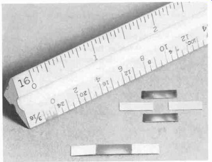
Fig. 301. Tape resistors are small and easily used. Their fiat character is
a space-saving feature. (Courtesy Hansen Electronics)

Fig. 302. The coaxial resistor, a variation of the tape resistor, is particularly
suited to high-frequency uses. (Courtesy Hansen Electronics)
Clean the surface of the base material thoroughly. Glass can be cleaned with ordinary household detergents. TSP ( tri-sodium phosphate) is excellent for soft plastics. Bakelite can be cleaned with carbon tetrachloride or chloroethylene.
Table 3-1. Properties of Low-Resistance Paint R11
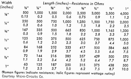
(Roman figures indicate resistance; italic figures represent wattage rating) Courtesy Micro-Circuits Co.
Resistance paints are available commercially. The advantage of using such mixtures is that they will give good results without the experimentation required when paints are home made. These paints are shipped a bit thin by the manufacturer to allow for solvent evaporation in storage and shipment. The drying time ranges from 34 to several hours at room temperatures ( 60-80°F.). Drying under heat lamps or in an oven will speed drying time. The paints must be stirred thoroughly before and during use. If they are allowed to settle, resistance values will he higher than normal.
In general, the resistance of any conductor can be calculated with the following properties in mind: The resistance is directly proportional to the length of the resistor; it is inversely proportional to the width and thickness of the resistor; it is a function of the carbon content in the mixture; the wattage rating is directly proportional to the surface area.
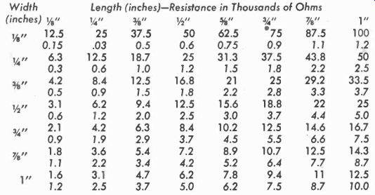
Table 3-2. Medium-Resistance Paint R21 (1,600 to 100,000 ohms) Width Length (inches)-Resistance in Thousands of Ohms (Roman figures indicate resistance; italic figures represent wattage rating) Courtesy Micro-Circuits Co.
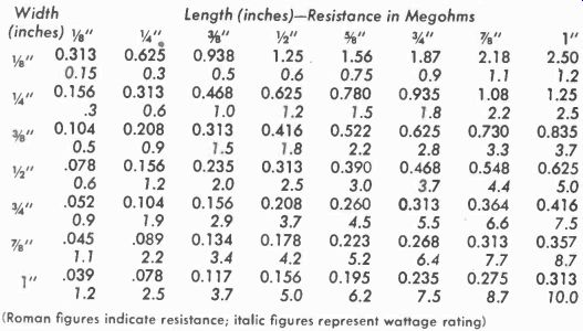
Table 3-3. High-Resistance Paint R31 (40,000 to 2,500,000 ohms)
The manufacturer controls the carbon content of commercial mixes closely, leaving the dimensional factors to the user.
The figures in Table 3-1, 3-2 and 3-3 are a guide to dimensions and ohmages of the finished resistor. In all cases, the calculation of ohmage is based on a resistor 1-inch square and 1-inch thick, having a unit thickness. The values given list resistor widths in increments of 3i-inch against progressive lengths of Ni-inch. At each intersection of a given width and length is the approximate resistance and under the resistance is the approximate wattage.
For example, in Table 3-1, let us take a resistor 3/4-inch by 5/8-inch long. The approximate final ( dry) resistance of a resistor made up in R11 paint' is 750 ohms. The corresponding wattage is about 3.7. Note that the same paint size resistor in R21 paint, Table 3-2, is 18,800 ohms and the wattage is the same. The resistance change has been accomplished in this case by the composition of the carbon mixture. A study of the tables shows three ranges of carbon content listed. Two others are available-a very low range R01, and a very high range R41. Specific directions for the use of these two mixtures are available from the manufacturer.
A good idea in setting up the resistance values is to draw out lines of the resistor first, using a soft lead pencil on the base material. The two "ends" can be painted in with silver-conducting paint. The resistance paint should slightly overlap the silver conductors. To obtain close values of resistance, one of the dimensions can be deliberately undersized and the resistance paint carefully added to bring the dimension to the exact size. Sanding or scraping with a razor blade can remove or add resistance, de pending on which dimension is altered.
Lower resistance can be obtained by adding several layers of paint, allowing each layer to dry thoroughly before adding the next.
Here are some tips on resistance-paint technique:
1. Be sure the paint is thoroughly mixed before and during use. Shake or stir occasionally during application.
2. If cracks appear in finished resistors, adhesion to the base material is probably poor. Remove the cracked resistor and clean the base thoroughly. Be careful not to smudge the base with fingerprints.
3. Make allowance for "wet" vs. "dry" resistance. The effects of drying on resistance are shown in Fig. 303.
4. Do not bake resistors until after they are partially dry. If any solvent is left and external heat is applied, the resistor may "bubble." Wait at least 15 minutes before baking.
5. Resistor thickness must be uniform if the resistor is operated near maximum wattage. If it is uneven, the thick section will over heat and possibly crack the resistor.
You may find that resistors do not follow the values given in the manufacturer's literature as closely as might be expected.
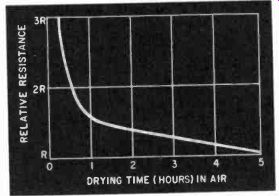
Fig. 303. Variations in resistance occur with drying time when resistance
paints are used. The final (stable) value is reached only when the paint is
thoroughly dry. (Courtesy Micro-Circuits Co.).
Many factors are responsible for this. For instance, the surface treatment must be standardized by the user for reproducible results. If a ceramic base is used and etched a certain way prior to the application of resistance paint, the same preparations must be made the next time the resistor is made. Likewise, if card board is used as a base material, an even coating of the same type of shellac or varnish must be applied to the cardboard base before applying resistance paint.
One test for consistency is to measure the resistance several times after drying. When the value remains constant, it can be assumed that this value is the final one. Carbon has a temperature coefficient ( i.e., its resistance changes with temperature) so the resistance will vary slightly with ambient temperature. This should not cause any trouble for most work at room temperatures.
Subminiature carbon resistors
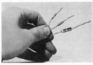
Fig. 304. Many varieties of carbon-composition resistors are commercially
available.
The conventional carbon-composition fixed resistor is also useful in printed-circuit work. Fig. 304 shows a representative sampling of fixed carbon resistors. Several physical forms are available commercially, including the uninsulated and insulated axial-lead types, and the radial-lug and radial-lead types. The most popular is the insulated axial-lead unit.
Common wattage ratings for printed-circuit uses are in the range of 1/5 to 1/2 watt, and one manufacturer has recently brought out a 1/10-watt unit. Wattage is roughly a function of size, but both will vary depending on the individual design. Lead length varies from 0.75 to 2.5-inches, depending on the end use of the resistor. Longer lead lengths are furnished for components used in automatic assembly machines or that have to be wrapped around terminals.
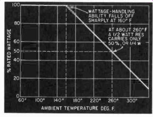
Fig. 305. Resistor derating curve. The wattage rating of resistances decreases
with rising temperature. (Courtesy IRC).
Insulated resistors are made in several ways. Some units have the resistance element laid down around a glass tube. Each lead has a small upset or flange on it. The two leads are inserted into the ends of the glass tube and pushed in. The flange prevents short-circuiting of the leads. The carbon-composition mixture is then put on the tube surface and the coating is extended on each end to make contact with the flange on the lead. Then the assembly is molded inside of a phenolic plastic.
In others the resistance element is formed, the leads inserted and the entire assembly is encased in plastic as one integrated manufacturing operation. Another method is to make the resistor and leads as a subassembly, insert that assembly in ceramic tubes and then cement the ends of the tubes, leaving the leads to come through the end caps which are cemented to the body assembly.
Any carbon resistor generates noise. Some of it is due to the agitation of molecules by heat (so-called Johnson thermal noise).
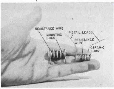
Fig. 306. Special wirewound resistors are manufactured specifically for printed
circuit purposes. Note the size of the units.
Other forms are produced when a direct current is sent through the resistor. Noise created by carbon resistors is usually measured as so many microvolts per volt of dc applied to the resistor.
An average figure for resistors in the 1/2-watt range and below is 2 to 5 microvolts per dc volt.
When running resistors above their normal temperatures, it is necessary to derate them ( Fig. 305) since most carbon-composition resistors have organic binders which decompose at elevated temperatures. It is sometimes possible to add a mass of metal to hold the resistor in place and this metal (called a heat sink) will help cool it.
Voltage ratings of composition resistors are determined by the strength of the dielectric material and the general design of the resistor body. Common carbon-composition resistors in the 3-watt range have voltage ratings around 300, but special units have been made which go up to 750 and 1,000 volts in the same wattages.
At high frequencies, a resistor will have properties that make it look like an inductor or a capacitor or combinations of both. The value of resistance usually changes with frequency and in general tends to drop off at higher frequencies. Rf bridges are used in one method of measuring resistance at high frequencies.
Selection of subminiature wirewound resistors
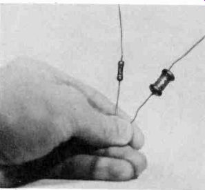
Fig. 307. Deposited-film resistors are manufactured for low-noise applications.
Typical examples of commercial wirewound resistors for miniaturized use are shown in Fig. 306. The usual construction is alloy resistance wire wound on ceramic tubes. The winding is then coated with organic cements or vitreous enamels. Resistance-wire materials used are the Nichromes (nickel-chromium), Manganins (copper, manganese, nickel) and Advance (nickel-copper) alloys.
The resistivity ( resistance per unit length and unit cross-section ) varies with the purity of the alloys and differences in the manufacture of the alloy wire.
One special class of wirewound resistors, the "accurate" group, have tolerances of better than 0.5%. These are usually hand-wound and checked for resistance with a Wheatstone bridge.
Deposited film resistors
Another manufacturing technique in fixed resistors is the use of conductive films laid down on a nonconductor base material.
These "deposited-film" resistors are shown in Fig. 307. The films are made of either metallic or carbon-bearing materials. The commonest are carbon and boron. Film type resistors find use in circuits where their low noise factor is important and where precision wirewound units in the 0.1% to 0.5% class are too expensive to use. Other uses include meter and voltage-divider circuits requiring high stability and high-frequency circuits in which wirewound units are unsuitable due to inductive or stray capacitance effects.
Flexible resistors
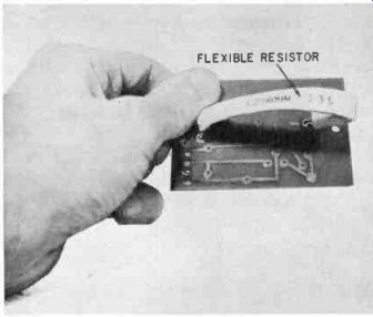
Fig. 308. Special high-wattage flexible resistors find wide application on
printed-circuit boards.
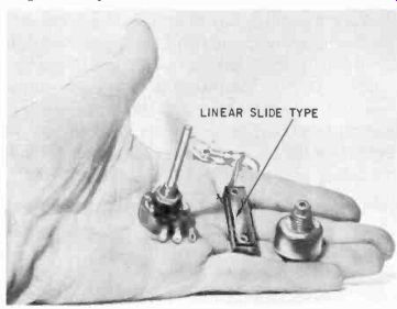
Fig. 309. Representative miniature variable resistances.
Fig. 308 shows a flexible resistor in use on a printed-circuit board. Developed to fill the need for a high-wattage resistor that 4,4 is mechanically flexible, these units are available in sizes from 1 to 10 watts-the rating being roughly 2 watts per inch of length.
They are normally wound on Fiberglas cores and have running surface temperatures of about 300°F at the hottest point.
Miniature variable resistors
Fig. 309 shows representative versions of miniature variable resistances. One form, the linear slider type, is adjusted by a screwdriver slot on one end. This type of unit usually has a clutching arrangement to prevent overtravel of the wiper and subsequent damage to the wire wound element itself. The power rating is between 3/4 and 2 watts and the terminals are often gold plated to cut down corrosion. Resistance values available range from 10 to 200,000 ohms with 5% tolerance as the standard or 1% tolerance available on special order. This type of variable trimmer comes with soldering lugs, pigtail leads and pins for direct mounting in printed-circuit base boards.
The miniature potentiometer shown in Fig. 310 is 1/4-inch diameter by 11/32-inch long. Rated at 3/4 watt, it takes about 500 such potentiometers to weigh a pound. Standard resistance values are 500, 1,000, 2,000, 5,000 and 10,000 ohms, and the winding is approximately linear with rotation.
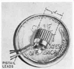
Fig. 310. A miniature potentiometer rated at 0.25 watt. (Courtesy Minelco)
A very common miniature variable resistance unit is the type shown in Fig. 311. First pioneered for hearing aids, these units have found their way into many printed-circuit and subminiature applications. Several varieties are made, the average of which is rated at 1/10 watt, measures 23/32-inch in diameter with its knob and 5/8-inch in diameter without it. Another subminiature model measures about 3/4-inch in diameter. Units are available with and without integral switches. Mounting is either by stud or bracket.
Resistances range from 500 ohms to 5 megohms with a choice of two resistance characteristics or tapers ( resistance vs. rotation curves ). These tiny units have a breakdown of 900 volts ac rms. A 3/4-watt unit is also made for solid- or slotted-shaft tuning.
[Manufactured by Miniature Electronic Components Corp. Manufactured by Centralab.]
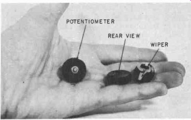
Fig. 311. Ceramic type miniature potentiometer.
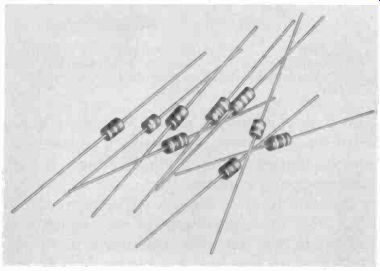
Fig. 312. Miniature ceramic capacitors have been available for a number of
years. (Stackpole Carbon Co.)
Capacitors for printed-circuit and subminiature use
The variety of capacitors suitable for printed-circuit and subminiaturization work has been limited only by the ingenuity of designers and our present technology. Of the three common circuit components-resistors, capacitors and inductors-capacitors are probably the group that has received the greatest attention in printed-circuit work. Materials with unusual dielectric strengths have been substituted for conventional wax and oil, with startling size reductions. Glass has been used both in fixed and variable capacitors. Newer plastics such as polystyrene in thin films have made possible variable capacitors one-half to one-third the size of conventional units used in ordinary five-tube ac-dc super heterodynes. The introduction of Mylar promises even greater gains in size reduction while increasing capacitances and working voltages.
Ceramic capacitors
One major group of fixed capacitors suitable for printed-circuit work are the ceramics. Some of these (Fig. 312) have been avail able for a few years. The units are molded with organic thermo setting binders and have normal values of 0.1 to 10 uuf. The body material is high-dielectric titanium dioxide, and the working voltages average about 500 dc. Typical applications include rf coil coupling and if transformer coupling. The leads of the units in Fig. 313 are designed to withstand a 10-pound pull.
Other ceramic miniatures have been developed with subminiaturization and printed circuitry in mind. The units, shown in Fig. 313, have vacuum wax-impregnated phenolic insulation.
Fig. 313. The fiat type miniature ceramic capacitor is very useful in printed
circuit work. Note the mounting tabs. (Courtesy Mucon.)
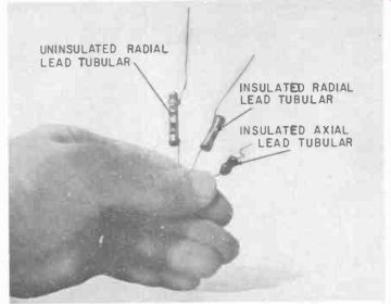
Fig. 314. The tubular ceramic capacitor is widely used in all branches of
electronics.
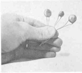
Fig. 315. Disc ceramics, such as those shown, are easily adapted for use in
miniature circuits.
Standard working voltages are 200 to 500 vdc. Although fixed in the sense that there are no moving parts, a capacitor is also made that changes capacitance with applied voltage. It finds wide use in tuning and frequency controls.
Another common form of ceramic capacitor is the tubular type shown in Fig. 314. The central part of the capacitor is a ceramic tube coated inside and out with conductive material. After lead wires are attached to the two conductive layers, the entire assembly is coated with an insulating dip. Tubular types are also made in the form of feed-through units for high-frequency circuits where lead length and lead dress is important. By various methods of manufacturing, the ceramic capacitor can be given different temperature coefficients. The major types are the negative or N-type, positive or P-type and the NPO or near-zero-type.
Fig. 314. The tubular ceramic capacitor is widely used in all branches of
electronics.
The N-type gives a decrease in capacitance with increase in temperature, the P-type is just the opposite, and the NPO-type does not change capacitance appreciably over wide changes in temperature. Thus, it is an easy trick to make a tank circuit or an oscillator very stable by the proper choice of ceramic capacitor.
Fig. 315. Disc ceramics, such as those shown, are easily adapted for use in
miniature circuits.
Various forms of disc ceramics, such as those in Fig. 315, offer capacitances in the order of 500 uuf up to about 0.1 pf in a very compact package. A variation in manufacture of this type consists of putting two or more units in one case by stacking single units before encapsulation in the insulating medium used for the body covering.
Metalized paper capacitors
The units shown in Fig. 316 are another development in paper capacitors. They use a metal-coated paper as a substitute for the common paper-foil sandwich. This metal-coated paper is usually a Kraft paper only 1/1,000 inch thick, and the metal coating is about 1/1,000,000 inch thick. Capacitors rated .05 to 5 of at 200 volts are about a third as long as a cigarette. Mineral-oil waxes are widely used sealers for this capacitor.
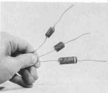
Fig. 316. Modern manufacturing methods permit the manufacture of paper capacitors
in sizes suitable for printed-circuit work. (Boughton-Callihan Enterprises)
Fig. 317. The mica capacitor, an old standby, has been miniaturized for use
in modern circuitry.
Mica capacitors
One of the "old-timers" in radio and electronics, the mica capacitor utilizes the dielectric properties of a natural mineral.
Fig. 318. Glass capacitors, smaller than micas of equal rating, provide humidity-proof
components.
Typical construction consists of mica sheets and metal foils arranged in sandwiches with the mica sheets alternating with the foils in the sandwich. Tin, silver and aluminum are common foil materials. The foils are paired to alternate common leads with the mica as spacing material. The whole assembly is then molded in Bakelite and the capacitance value color-coded on the body. Common capacitance tolerances are 20%, 10% and 5%, with the silver mica units rated as the most stable with changes in temperature.
Typical mica units suitable for printed-circuit and allied work are shown in Fig. 317. Improved design and materials permit capacitances as high as 4,000 uuf at 500 working volts dc in a unit only 7/16-inch wide by 3/4-inch long by 3/4-inch thick.
Color codes on mica capacitors have been changed several times, and it is best to consult the particular manufacturer for in formation on coding. Some manufacturers stamp the capacitance value into the body during the molding process.
Fig. 319. When glass is used in the manufacture of capacitors, extremely high
voltage ratings are possible, even with miniature units. (Courtesy Corning
Glass Works.)
During World War II, a serious question came up concerning the continuing supply of mica from India, which has been the largest source. As a result of military-sponsored research, a series of high-quality dielectric glasses for making capacitors was developed. Some of these are shown in Fig. 318. Glass capacitors require many unusual glass-manipulating techniques. The glass is formed into a thin ribbon and, during capacitor assembly, the glass ribbon and a metal foil are sandwiched together to give the required final capacitances. Terminals are added and the entire capacitor units are pressed out like soda crackers. The glass body holds the dielectric sandwich rigidly and capacitance values are more stable than for mica units under similar temperature and vibration conditions.
A glass capacitor is usually smaller in volume than a mica unit of the same capacitance at the same working voltage. Q's of high-capacitance glass units do not drop off as rapidly as those of mica units at higher frequencies and the glass construction eliminates the wax impregnation used on micas for humidity-proofing. Glass capacitors designed for high-voltage use are shown in Fig. 319.
Electrolytics
Fig. 320. Quite a departure from the familiar-electrolytic, the miniature
capacitors shown are about the size of ordinary tubular capacitors.
Fig. 321. The glass and quartz piston capacitor finds wide use because of
accuracy and ease of mounting. (Courtesy Corning Glass Works.)
Electrolytic capacitors are made of two electrodes, most commonly aluminum, separated by a liquid or semi-liquid conductor.
The dielectric element is a thin film formed on the anode. The commonest "dry" electrolytics used in radio and television work consist of aluminum foil separated by the electrolyte which is made up as a paper or blotter separator. The separator is saturated with electrolyte and the foil-and-blotter combination is rolled up like a jellyroll and encased in a waxed cardboard or metal case. Various forms of electrolyte are used, ranging in viscosity from liquids to heavy pastes. The insulating film is formed on the anode by the application of external voltage.
One very interesting feature of electrolytics is polar and non-polar construction. A non-polar unit is used in circuits where there is a reversal of polarity. The more common polar, or polarized, units are used in dc circuits where no reversals occur. Capacitance for a given volume is less for a reversible ( non-polar ) electrolytic than for a polar unit with the same voltage rating.
Tantalum capacitors
Fig. 322. A commercial printed-circuit oscillator using a piston type capacitor.
(Courtesy JFD.)
Another development in electrolytics, the tantalum unit has several advantages over ordinary aluminum types. The corrosion resistance of tantalum is higher than aluminum, permitting the use of more active electrolytes. Tantalum oxide films, the dielectric in these units, are more stable than their aluminum counter parts. Tantalum units can also be used at higher temperatures and will go down to lower temperatures with less loss in capacitance. Tantalum units generally have a lower dc leakage than does aluminum. Leakage tests are usually made by charging the capacitor for several minutes and then measuring the current flowing through the unit after 5 minutes or so. A series resistor is used to limit charging current to a safe value.
In all fairness to aluminum units, however, tantalum still has a few disadvantages. One of these is high cost per unit of capacitance. Another is that present units with capacitances over 1.0 of are limited to approximate working voltages of 150 vdc.
Electrolytics are subject to failure from excess heat, long shelf storage, and occasional pinholes and defects in the electrode foil material. Polarized units should be carefully checked for proper circuit connections; otherwise they may be ruined or, if over loaded too long, they may explode.
An assortment of miniature electrolytics is shown in Fig. 320.
Variable capacitors
For capacitances in the range of fractions of 1 uuf up to about 50 1.10, the glass and quartz piston capacitor finds wide use. The units shown in Fig. 321 are representative. A piston of ferromagnetic material is arranged to slide in and out of a metalized glass or quartz tube. The two concentric elements act as a capacitor.
Various features claimed by manufacturers of such units are vernier adjustment to increments of as little as .05 uuf per turn of the adjusting screw, no tuning, backlash, wide operating temperature range (-90° to +450°F. ), silver plating for higher Q's, and high dielectric strength for use on circuits up to several thousand volts dc. The most advanced designs employ quartz tubes and invar rotors. Fig. 322 shows one of these units in a printed-circuit oscillator.
Concentric shield units A unique design permitting variable capacitance up to 50 uuf in small spaces is shown in Fig. 323. The concentric shield capacitor has a Q of about 75 at 27 mhz and can be tuned with a knob or extension shaft made of plastic.
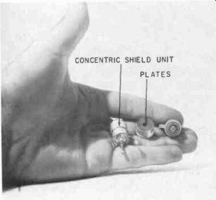
Fig. 323. The concentric-shield variable capacitor is an extremely compact
unit.
Fig. 324. Ceramic trimmer capacitors are well suited to printed circuits.
They are extremely stable and are minimally affected by mechanical shock.
Ceramic variables
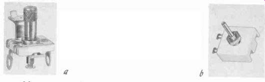
Fig. 325. Mica compression trimmers mi easily adapted for miniature work;
a) knob-tuned unit; b) shaft-tuned type. (Arco.)
Manufactured for years for conventional trimmer uses, the variable ceramics shown in Fig. 324 are ideal for printed-circuit work. Mounted on ceramic or steatite bases, they provide capacitances up to about 60 ijf in various mounting styles. These ceramic trimmers offer high stability under vibration due to the lightweight rotor which is kept under heavy spring pressure. The rotor and stator surfaces are ground optically flat to eliminate troublesome air films between them.
Mica trimmers
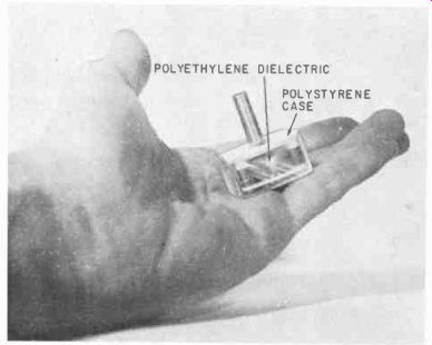
Fig. 326. Meshed-plate variable tuning capacitor. Completely enclosed, the
unit uses polyethylene sheets between the plates. (Courtesy Argonne Electronics
Mfg. Co.).
Mica compression trimmers can be adapted to printed-circuit and subminiature uses. Variations include dual and multiple units, half-size units in which the width of the body is about one-half normal size, and knob and shaft tuning units. The latter two types are shown in Fig. 325. Capacitances range from 3 to 30 uuf in two-plate units to 1,200-2,600 uuf in units with 15 plates.
Ratings vary from 250 to 500 volts working dc with a 1,000-volt test for flashover.
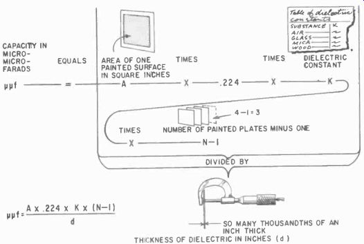
Fig. 327. Step-by-step process involved when calculating capacity. The formula
is especially useful when fabricating capacitors.
Mesh-plate units
The meshed-plate variable capacitor shown in Fig. 326 is one of the major advances in subminiature variable capacitor designs made as a result of printed-circuit and space demands from manufacturers and amateurs. A polyethylene dielectric is used between plates, and the entire plate assembly is enclosed in polystyrene.
The polystyrene case prevents entry of dust and also houses two rotary type trimmers which are adjustable through holes in the rear cover. In addition, body-capacitance effects are cut down by insertion of shielding plates in the rear of the unit when the unit is mounted on a metal chassis. Another novel feature is 175° rotation instead of the conventional 180°. The 5° limit on rotation prevents damage to the polyethylene film in case the rotor plates fall out of mesh with the stator plates. Maximum capacitance of the two-gang unit is 211 uuf in the antenna section and 101 uuf in the oscillator section. Minimum capacitances of the same sections are 13 and 11 uuf, respectively. Breakdown voltage is 50 volts dc after 1 minute. The Q is over 2,000 at 1 mhz. The trimmers range between 12 uuf minimum and 50 uuf maximum.
Single-and three-section 365-uuf units are also available. The latter are only 1-1/16-inches square by 13/16-inch deep. The manufacturer claims all units in the line have a life of over 10,000 operations without appreciable capacitance shift.
Making your own printed and etched capacitors
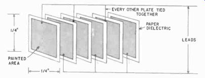
Fig. 328. Practical application of the formula illustrated in Fig. 127.----
Practical Example of Formula Capacitor has 6 plates. Each plate is 1,'t inch
square. The dielectric is .006-inch thick paper. Find the approximate capacitance.
Printed or etched capacitors are limited with present techniques to capacities in the 1-200- uuf range. In general, the formula for the area of a conductor-dielectric plate sandwich type capacitor is ...
c X d A- 0.224K(n-1)
... where A is the area of one painted or etched surface in square inches; K, the dielectric constant of the separating material; d, the thickness of the dielectric ( separator) in inches; n, the total number of painted or etched plates; c, the capacity in uuf of the entire capacitor. The use of the formula is shown in Fig. 327. A practical example is shown in Fig. 328.
Dielectric constants vary from 1.0 for air to about 7 for celluloid among the more common materials. Typical dielectric constants for materials found around the shop or home are given in Table 3-4.
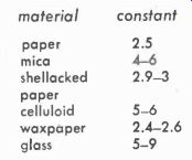
Table 3-4. Dielectric Constants of Common Materials
material: constant:
paper 2.5 mica 4-6 shellacked 2.9-3 paper celluloid 5-6 wax paper 2.4-2.6 glass 5-9
Voltage breakdown for a capacitor depends on dielectric strength ( not to be confused with dielectric constant ). For card board, this would be about 100 volts per mil ( 1/1,000 inch ). If there were four plates, each 15/1,000 inch thick, then the total thickness would be 60/1,000 inch. The theoretical voltage break down would be 60 X 100, or 6,000 volts. However, a safety factor of at least 10 should be applied to home-made units. This would give a working voltage of 600.
Subminiaturization and inductors
Inductors have been very difficult to miniaturize, requiring new techniques in wire drawing, insulating and winding. The printed and painted inductor has many limitations and must share a great deal of application with inductors that still use wire.
Nevertheless, the conventional receiver intermediate-frequency transformer can, normally a good 13k-inches square by 3-inches high, has been shrunk to a pygmy unit as a result of several years of effort. The search for higher inductance in smaller volumes has also led to the development of new core materials having permeabilities in the hundreds as compared to air. Metallic films and foils deposited on dielectrics have also been used as coils with limited values of inductance in the microhenry and low milli henry ranges. The recent discovery of materials with permeabilities in the thousands and finer wire-drawing techniques offer promise of inductors the size of match heads with millihenry values. As just one sideline, the art of electronic computers is depending heavily on such components for large quantities of stored information in tiny spaces.
Inductive components
Fig. 329. Construction of miniature transformers seems to be conventional.
It isn't. Special techniques are required. (Courtesy United Transformer Corp.)
Probably the most familiar of all subminiature inductors are the transformers shown in Fig. 329. These have plastic-insulated wire on nylon bobbins and use high-grade electrical steels in the ferromagnetic part of the assembly. Transformer designs this small demand special metallurgical techniques such as grain orientation in the steel and heat treatment in gas atmospheres. All of these processes are necessary to achieve acceptable frequency response characteristics for uses such as hearing aids and miniature radios. Many miniature transformer manufacturers employ alloys of iron and nickel for the lower wattage units and specially treated silicon steels for the higher-wattage transformers. Note that we are talking about transformers designed to handle milli watts-and in extreme cases, in power transistor circuits, a few watts. The problems of distributed capacitance and leakage reactance effects in these tiny units are minimized by special windings such as interleaved windings-a cousin to the old-fashioned "honeycomb" winding.
Pickup of outside signals by induction is a common problem in transformers of this size and power level. One approach to this problem employs two balanced coils which tend to neutralize stray pickup. Multiple shields of high-nickel alloys are also used to attenuate hum.
An extreme example of subminiaturization in transformers is shown in Fig. 330. Measuring only 5/16-inch in diameter by 13/32-inch long, it would take over 150 of these units to weigh a pound. The leads of the unit are insulated with a plastic that melts in the course of soldering the unit into a printed circuit.
It is also hermetically sealed and the leads are designed to with stand a 10-pound pull. Depending on the source and load impedances, the transformers have a reasonably flat response in the 300-5,000-cycle range; a typical response curve is shown in Fig. 331. They are available in input, interstage and output de signs and have been made with center-tapped windings. De signed mainly for transistor circuits, the input impedances range from 150 to 200,000 ohms, and output impedances vary from 3.2 ohms for speaker matching to 2,500 for interstage coupling.
Power levels range from 25 to 500 milliwatts.
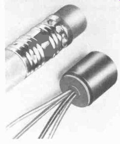
Fig. 330. Among the smallest of the small, this transformer is the size of
a pencil eraser. (Courtesy United Trans former Corp.)
Rf inductors
The maximum inductance of printed-circuit coils is usually limited to 100 microhenries or less in the simple single-layer construction; higher-inductance multilayer printed coils are usually plagued by low Q effects. However, three-dimensional rf chokes ...
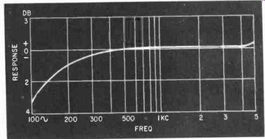
Fig. 331. Typical response curve for a transformer such as shown in Fig. 330.
(Courtesy United Transformer Corp.)
... have been designed that fit printed circuit and miniature applications nicely.
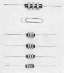
Fig. 332. Typical fixed-inductance rf chokes which can be used in miniature
equipment. (Courtesy Superex.)
Typical fixed-inductance-value rf chokes are those shown in Fig. 332. These units have pi-wound coils on ferrite cores. The pi-wound construction reduces distributed capacitance and the cores produce higher inductance in a fixed space.
A variable inductance design is shown in Fig. 333. The core has been mounted on a threaded stud, permitting adjustment of the core position within the coil. The range of inductance for coils in such designs varies from 40-250 microhenries in the smaller sizes to 0.25-0.5 henry in larger sizes.
Fig. 333. A variable inductance. The core is movable by means of the threaded
shaft. (Courtesy Superex.)
A pair of key components in subminiaturization, especially in superheterodyne circuits, are the if transformer and the oscillator coil. Examples of these are shown in Figs. 334 and 335. Several coil manufacturers have produced ifs 3i-inch square by %-inch high, and the most recent units are approximately 1/4-inch square by 3i-inch high. Q values run up to 150, and many of these tiny ifs have built-in shunt capacitors. One typical if unit for transistor circuitry has a primary impedance of 25,000 ohms and a secondary impedance of 600 ohms. The oscillator coil shown will tune with oscillator sections of variable capacitors having only 75-100 uuf maximum capacitance in contrast to conventional values of 170 to 210 uuf.
Fig. 335. A miniature oscillator coil.
The if coils shown in Fig. 336 are examples of plug-in types suitable for TV if strips. They are encapsulated in resin to exclude moisture and dirt, and have adjustable cores.
Loop antennas
The loop antenna that was commonly found in the five-tube ac-dc superhet and usually taking a space about 6 by 8 inches has been improved for miniature circuitry by using ferrite cores.
Fig. 334. Miniature if coils designed to be mounted on a printed-circuit board.
Fig. 337 shows one loop antenna design using a core 5 inches long by % inches in diameter. The Q for such a unit is about 500, and the inductance is 425 microhenries. The coils are impregnated with beeswax to seal out moisture. The unit mounts by means of a bracket.
Another antenna design utilizes a flat ferrite slab. This unit, shown in Fig. 338, is available in several inductance values, the two most common being 230 and 397 microhenries, designed to tune the broadcast band with 365- and 210-puf capacitors, respectively. This flat type antenna is usually mounted on brackets by cementing or by wrapping a few rubber bands around the flat surface near each end of the coil. Q's of flat units vary from 200 to 350.
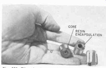
Fig. 336. The plug-in type if coils are extensively used in TV. These units
are potted. (Courtesy Essex Electronics Co.)
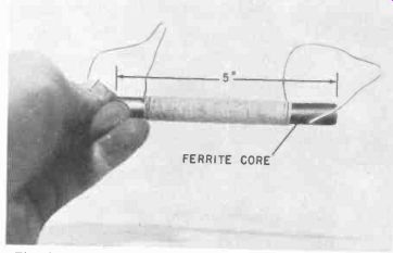
Fig. 337. One type of ferrite-loop antenna used in miniature circuitry.
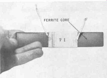
Fig. 338. Flat ferrite rods are also used in loop antenna designs.
Matched-coil kits
A matched-coil kit is available which consists of three 455- khz if's, an oscillator coil, a ferrite loop antenna and a subminiature two-gang capacitor. The entire kit is designed for use in superhet circuits using transistors. The shielded oscillator and if's are only 7/16-inch high above the chassis and about 3/4-inch in diameter.
The oscillator coil has an inductance of 261 microhenries which can be varied by ±20% with a tuning slug. The unloaded Q of the oscillator coil is approximately 140, and distributed capacitance is 7 uuf. The first if or converter output coil has a primary impedance of 15,000 ohms and a secondary impedance of 250.
The second and third ifs have similar primary impedances but slightly different secondary impedances. The subminiature two- gang capacitor is a polyethylene-coated plate unit, as described previously, and is matched to the antenna inductance in one section and the oscillator inductance in the other. The entire kit is shown in Fig. 339.
Glass inductors (metalized)
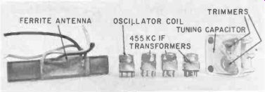
Fig. 339. A matched-coil kit consisting of if's, oscillator coil, antenna
and tuning capacitor. Note the size of the units.
Designed for use at 25 mhz and above, the metalized glass inductor shown in Fig. 340 offers the advantages of high tempera ture stability due to the low expansion coefficient of the glass form and the low temperature coefficient of the glass dielectric. Q's average 150. Typical specifications for such units would be: frequency, 38 to 49 mhz, Q at 50 mhz ( without core) of 150, apparent inductance of about 1/3 microhenry at 50 mhz, and average distributed capacitance of coil approximately 1.6 uuf. The ends of the metalized windings are tinned for soldering. Double-pitch windings are available for rf transformers and inductive coupling. Turn spacing varies from just under 1/32 to as high as M inch.
Making your own printed-circuit inductances In general, single-plate printed-circuit inductors are limited to inductance values below 100 microhenries. However, multi layer inductors can be built up to higher inductances by insulating between layers and coupling coils together. One limitation of the multi-layer construction, unfortunately, is the Q obtainable.
Another bothersome effect is distributed capacitance.
For single-layer inductances, three geometric forms are popular. The first of these is the circular coil printed on a section of tubing of which the outside diameter is relatively uniform. A practical application of this type of coil is given in Section 7 in the "lipstick transmitter circuit. There a coil has been painted on the glass envelope of a vacuum tube with silver paint. One formula for such a coil is:
ph ..025xkxdXN2 XL
These symbols simply mean that the inductance in microhenries is equal to the five quantities, .025, k, d, N2 and L multiplied together. The formula is explained in Fig. 341.
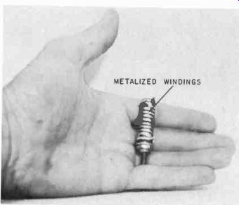
Fig. 340. Metalized glass inductor offers high tempera ture stability
Another popular design is the flat spiral shown in Fig. 342.
The spiral starts out at some central point and moves outward in rings of increasing size to a point on the outside. A riveted connection or eyelet drilled in the inductor acts as a termination.
One formula for the spiral inductor is:
ph=.02 XN2 XdXp ... where ph is the inductance in microhenries; N, the number of turns p, the permeability of material in and around the core (p is 1 for air), and d, the mean diameter of the coil.
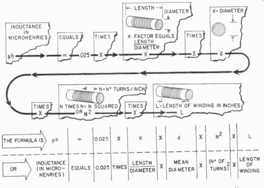
Fig. 341. Method of finding the inductance of a single-layer coil.
Mathematical formulas may be a bit baffling, but Fig. 343 takes most of the mystery out of this one.
Fig. 342. Example of a flat-spiral inductor.
Fig. 343. How to figure the inductance of a spiral in duct or.
Fig. 344. The flat square is another form of inductor.
A third form of inductor, the flat square shown in Fig. 344 is easier to draw and offers experimenters another variety in layout.
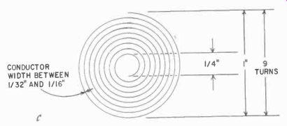
Fig. 345 shows how to figure the inductance of circular and square type spiral
inductors. This method is based on work done by Harold E. Bryan of the Naval
Electronics Laboratory, San Diego, Calif.
1. Decide on the approximate size of the coil and select an inside and outside diameter as shown in Fig. 345-a. For example, let's choose an outside diameter of 1-inch and an inside diameter of 3/4-inch.
How to Figure the Inductance of a Spiral Inductor:
Coil has inside diameter equal to 1/4 inch, and outside diameter equal to 1 inch. No. of turns is 6. Find the inductance.
Step 1. Mean diameter, d, is
2. Compute the quantities a and c; outside diameter + inside diameter 1 + 34 5 a= 4 4 16 outside diameter- inside diameter 1-3/4 3 c- 2 2 8
3. Divide a by c or 5/16 % = 5/6 or about 0.83
4. Find 0.83 on the a/c scale ( Fig. 345-b )
5. Pick out the inductance ( in microhenries) desired. Find this value on the L scale. Assume we are using a value of 1.2 ph and are working with a circular coil. We use 1.2 on the right-hand side of the scale.
6. Draw a line joining 0.83 on the a/c scale with 1.2 on the L scale. This line intersects the index line at a point, X.
7. The original a value was 5/16 which is about 0.3. Locate this value on the a scale ( Fig. 345-b ).
8. Draw a line between 0.3 ( a scale) and X. The point at which this line crosses the n scale is the number of turns required. In this case about 9.
9. Lay out the coil by painting or etching as shown in Fig. 345-c. If we wanted a square coil we would use the left-hand side of the L scale in step 5. This would result in slightly fewer turns.
Q values of inductances The Q of a printed-circuit coil is generally lower than that of a conventional wire coil of similar dimensions. This is due mainly to edge effects, a rough edge tending to produce more rf losses than a smooth one. Higher Q's are possible with materials having Teflon or silicone-glass bases. One method of improving Q is to silver-plate the inductor. This can be done by electroplating or else by rubbing a paste of silver chloride or silver nitrate on the copper coil pattern. Because of the many factors affecting Q, actual tests on individual assemblies with Q meters are recommended. In the absence of a Q meter, use a grid-dip oscillator and a vtvm, as shown in Fig. 346.
Fig. 345. How to calculate the inductance of square and circular type inductors.
Use the chart on the facing page. (Courtesy Chilton Publishing Co.)
---------------
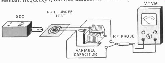
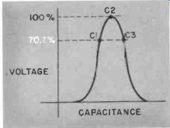
Fig. 346. Method of testing the Q of a coil, using a vtvm and a grid-dip oscillator.
To Find the "Q" of a Coil
1. Tune the capacitor for highest voltage, C2, on a vtvm
2. Detune to get 70.7% of C2 on low side (Cl)
3. Detune in the opposite direction to get 70.7% of C2 on high side (C3)
4. "Q" is then figured as equal to:
2 X C2 (C3 – C1)
The values of C1, C2 and C3 can be in uuf or uf. All values must be in same units, however. If C1 & C2 are in ,uuf, C3 must be in uuf.
---------------------
Distributed capacitance
All inductors have some distributed capacitance which makes them look like a tank circuit (L-C) at certain frequencies. At low frequencies, the inductance tends toward its true or dc value due to distributed capacitance effects. At some frequency, the inductance will resonate as a tuned circuit with its own distributed capacitance. The graph in Fig. 347 shows that, for a given inductance and distributed capacitance ( and therefore a fixed self-resonant frequency), the true inductance divided by the effective inductance increases as operating frequency decreases. Another way of looking at it is that, as the operating frequency is raised toward the self-resonant frequency, the effective inductance increases.
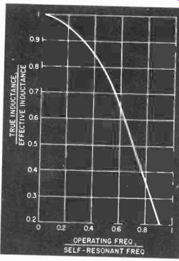
Fig. 347. Chart shows the relationship between inductance and frequency.
(Chilton Publishing Co.)
Use of magnetic materials The inductance of printed-circuit inductors on a dielectric surface is usually low because of small size and surrounding permeability. One side of the inductor is very often exposed to the air and the other side is on the insulating dielectric-both mediums having low permeability.
Several techniques have been employed to raise the permeability in such cases.
One method is to take out some of the center turns of the inductor and apply magnetic paint to the central portion of the coil.
Such a paint consists of a colloidal suspension of magnetic particles with appropriate binders and solvents. Another version of magnetic paint is a paste.
A second method for applying the magnetic material is to spray it on the inductor after insulating it from the magnetic paint by resin or very thin paper. In another technique, the base plate of the inductor is molded with a slot or cylindrical indentation, and a small slug of magnetic material is arranged to fit in the hole. A fourth technique consists of painting a magnetic disc on the insulating base plate of the inductor and then applying another magnetic disc to the opposite side of the inductor, sandwiching the inductor between the two. A further variation of the dual-disc method is to make two magnetic-disc inductor combinations and arrange them to slide over or past each other to vary the inductance. Inductors can be painted on conventional slug coil forms, and a wound inductor and painted inductor of approximately the same value are shown in Fig. 348.
Fig. 348. A wound inductor and a painted inductor of the same value. Note the difference in size.
The total self-inductance of two coils in series is the sum of each of the inductances plus two times the square root of the product of the inductances. Thus, if two similar inductances are used, say 2 microhenries each, the total self-inductance will be 2 ph + 2 ph 2 ,/ 2 X 2 ph, or 4 times that of each coil, or 8 ph. This could be done if two similar coils were painted on each side of the dielectric and connected in series. However, the Q of the circuit would be lower than single-coil construction, due to flux paths in the dielectric.
Rf coil forms-winding your own coils
Fig. 349. A variety of coil forms are available for those who want to wind
their own.
Shown in Fig. 349 are some empty coil forms which can be used by the experimenter who wishes to wind his own. Two main factors affect coil design. The first is the coil winding itself, and the second is the effect that the core will have on the inductance.
The four major types of magnet wire available to the experimenter are enameled, single cotton enameled, double-cotton covered and silk-covered wire. Ordinary enameled wire is made with a baked-on resin which is like household paint. The single cotton enameled is similar to the plain enameled wire, but has a single layer of cotton wrapping over the enamel. The double cotton-covered material is bare copper wire with two layers of cotton cord wrapped over it. The silk-covered wire is becoming less common: the extra cost of silk is seldom practical.
In using the cotton- or silk-covered wire, remember that textiles are porous. Coil dopes are used to keep out moisture and dirt.
Another important point to remember is to stick closely to any information which affects the number of turns or type of insulation, if exact results are expected the first time. This is especially true where construction articles specify a certain length of winding. Using enameled wire of the same gauge will give more total turns per inch than double-cotton-covered wire. This will affect the inductance and also any frequency characteristics such as being used with a fixed capacitor to tune to a certain frequency.
Most magnet wire coverings can be stripped easily with fine sandpaper or chemical solvents. Some of the plastic-covered wires can be stripped with a hot soldering iron.
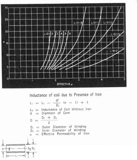
Fig. 350. Effect of cores upon the inductance of coils. The chart and formula
are used to calculate effective inductance and permeability. (Courtesy Stackpole
Carbon Co.)
Cores
The presence of a permeable material will change the inductance of a wound component.
Another factor that enters into coil calculations where there are cores is the length-to-diameter ratio.
A set of formulas and a typical family of curves which help predict the effective permeability and also the effective inductance are shown in Fig. 350. Once the effective permeability and L/D ratio are known, the inductance is calculated from the formulas. The actual permeability is determined by the physical nature of the core material.
Iron cores are made by mixing iron particles, 1 to 40 microns (0.001 millimeter) in diameter with a binder and then molding the mixture into shapes such as shown in Fig. 351. Various iron powder types are used. Some of these are produced by decomposition of iron carbonyl, by grinding iron mill scale and by reduction of iron oxides. Advantages of using iron cores, especially in high-frequency circuits, are ( 1) they reduce the number of turns of coil required for a given inductance, ( 2 ) they reduce stray flux and help boost Q's and ( 3 ) they produce coils with smaller distributed capacitances. Design factors influencing core selection center around the properties of the iron, and cores are usually classified into frequency ranges of use. The iron core will add some losses to the finished coil, and these must be balanced out with decreased copper losses due to eliminated copper coil turns and eddy currents in the core itself. For serious work, the core manufacturer should be called upon. Recent advances in core manufacture have produced a series of metallic oxide-ceramic combinations that have up to 10 times the permeabilities of iron cores.
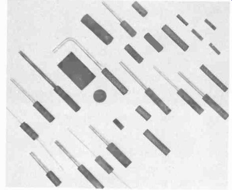
Fig. 351. Various types of molded iron cores. (Courtesy Superex).
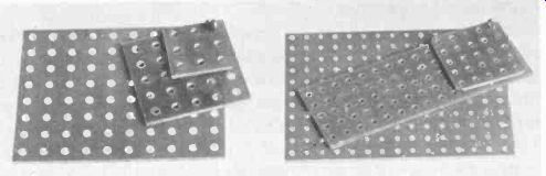
Fig. 352. Punched terminal boards, available in a variety of sizes and shapes,
are useful for permanent construction and experimental setups. (Vector Electronic
Co.)
Vital to the construction of any printed-circuit or subminiature assembly is the hardware that holds components in place. Like components, some hardware is conventional and has been scaled down for a particular use. Other units have been modified slightly in form or shape for printed circuitry. Finally, a unique class of hardware has come into existence designed for printed circuits and subminiaturization.
Punchboards
Terminal punch boards (Fig. 352) are used for quick mounting and test setups. These boards are available in several sizes, pat terns and materials. One pattern has a hole diameter of about 3/32 inch spaced on 33/64-inch centers and comes in either 1/16 or 3/32-inch thick material. Another has 1/16-inch diameter holes on 3/16-inch centers.
Fig. 353. Punched boards featuring stitched and tape wiring. (Vector Electronic
Co.)
Fig. 554. An example of a pre-etched circuit board for use with special printed-circuit
connectors. (Techniques, Inc.)
Stitched wiring boards
Stitched wiring is a form of breadboarding in which the connecting wires are fed in under eyelet and terminal boards in any direction and stitched in place like sewing. Wire stitching has the advantage of flexibility in the run direction. The technique permits runs on both sides of a breadboard. Several stitched boards can be wired up with vertical riser conductors, producing a modular structure. In cases of small experimental-quality runs, stitching is usually less costly and time-consuming than etching, especially where the number of wires ( wire-density) is low.
Tape stitching is another variation of wire connecting and is confined to straight conductor runs with bends at an angle. This type of stitching finds use as a ground bus, and is a cousin to earlier die stamping techniques.
Both wire and tape stitching are shown in Fig. 353.
Pre-etched test boards
Fig. 354 shows a facsimile of a pre-etched unit designed for use with printed-circuit connectors having 5/32-inch contact spacing, 1/16 inch wide. The material used in the actual board is 1/16-inch XXXP laminate with .00135-inch-thick copper on one side.
The pads or circles are 1/8 inch in diameter, and several models of the board are available with different rows of pads on different grid layouts. The pads can be drilled by the user or furnished drilled with No. 55 ( .052-inch) diameter holes. Manufacturers also make test boards for diode and resistor networks. The experimenter can duplicate any similar patterns in small quantities by etching methods.
Sockets
A versatile socket for breadboards is the surface type shown in Fig. 355. The surface type socket is especially suited for breadboard construction.
Fig. 355. In addition to the regular female socket contacts, this unit has
male lugs in parallel with the regular pins. The base connections are numbered
and the contacts are usually silver-plated phosphor bronze.
The right-angle socket was developed to save room in certain printed-circuit board layouts and also permit a more flexible arrangement of components. Several versions of this socket are shown in Fig. 356. One commercial design has buttress-ribbed construction to give the associated panel more rigidity.

Fig. 356. Right-angle sockets save space and permit flexible arrangements
of other components. (Cleveland Metal Specialties Co.)
Fig. 357. In-line and round-type subminiature sockets are used with tubes
and transistors.

Fig. 358. Some of the special multiple circuit connectors used in miniature
work. (Courtesy Circon Component Co.)
A variety of subminiature sockets are shown in Fig. 357. The ones on the left are known as in-line types and those on the right are round designs. Major problems in the application of these sockets are spring-contact design, corrosion and lead identification. Contact materials are usually phosphor bronze, brass or beryllium copper, with cadmium and gold most often used for plating. Body compositions are mica or mica-phenolics. Lead identification is made by either an orientation bump or colored dot on the in-line types; the round types are keyed on the socket base.
Connectors
Multiple-circuit male and female connectors for printed-circuit work are shown in Fig. 358. The variations possible include con tact spacing, contact spring design and mechanical mounting features. One miniature-series female connector has 5/64-inch con tact spacing with 12 contacts in a block about 1-3/8 x 7/16 x 1/4-inch. Another is based on 5/64-inch centers to produce a female connector just under 1 inch long, 5/16-inch wide by 1/4-inch thick. Contact arrangements come in 8, 12, 16, 32, 48 and 60 contacts with plating and materials to suit the user. Contact materials are spring brass and beryllium copper. Hoods are also available to protect the wires entering the connector.
Miniature coax connectors are shown in Fig. 359. These are made in various impedances, the most common being about 50, 52, 70 and 90 ohms. Cables as small as 1/16-inch outside diameter can be terminated with these connectors. Teflon is used quite often as the dielectric.
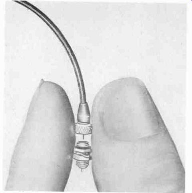
Fig. 359. Miniature coaxial 'connectors are available in a variety of styles
and impedances. (Amphenol-Borg Electronics Corp.)
Terminals One form of clip-in terminal, shown in Fig. 360, depends on serrated slots to grip the lead wires. These terminals do not require soldering in temporary setups. They are made in three forms known as the side-zip, edge-zip and push-in type. The edge- and side-zip units are fastened to 3/32-inch-diameter holes with eye lets, and the push-in type slips directly into a 3/32-inch-diameter hole without eyelet.
Fig. 360. Clip-in terminals require no soldering when used in temporary circuits.
(Vector Electronic Co.)
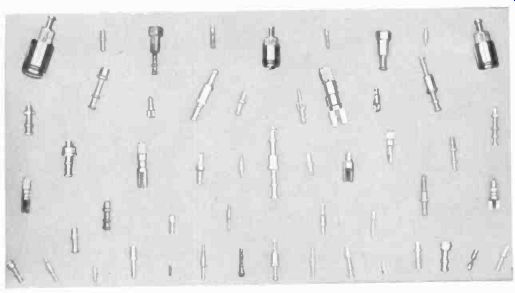
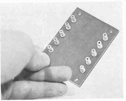
Fig. 361. Staked terminals (above) are mounted to circuit boards (below) by
a process similar to riveting. (Courtesy USECO)
The side-zip terminal has the serrated slots mounted to take components both parallel and at right angles to the base board.
The eyelets which hold the terminal can also be used as soldering points for vertical jumper wires or risers between decks of boards.
The edge-zip unit has serrated slots made to take components only parallel to the base board. The side-zip terminal has to be offset in some setups to avoid riser and component interference, whereas the edge unit has its eyelet hole offset to eliminate this problem.
Another feature of the edge- and side-zip units is a small strap ping fork. This serves a double purpose. First, it permits mating of adjacent terminals when the tongue of one terminal is locked into the fork of an adjacent one with needle-nose pliers. Secondly, it provides a tie or loop point for small-gauge wiring, No. 24 or thinner.
Fig. 362. The flea clip is a widely used connector in miniature circuitry.
Fig. 363. Spring flip component holder. (General Cement Mfg. Corp.)
The push-in terminal is inserted into 3/32-inch-diameter holes with needle-nose pliers. The terminal is formed from sheet brass and the half-tubular end holds the terminal in the base board tightly. A feature of this type terminal is .the slot in the inserted end. This slot can be used to hold additional component leads or can be staked into the base board permanently to hold the terminal. Flaring or staking can be done with needle-nose pliers.
The slotted tubular section can also be snipped off with side cutters close to the underside of the board.
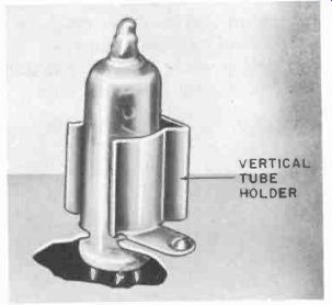
Fig. 364. Component holder for vertical support. (Atlas E-E Corp.)
The snipping action tends to flare out the tubular section and bind the terminal in place.
Various forms of terminals, designed expressly for staking into a base board, just like riveting, are shown in Fig. 361. These are usually made from brass, which can be electroplated with tin, tin and lead alloys, cadmium and gold. These terminals can be hand-swaged for small runs or mass-produced swaggering can be made with motorized equipment. A terminal board using swaged terminals is also shown in Fig. 361. These boards come in nylon, paper and cloth laminates, and other materials bonded with resins such as silicones, phenolics and melamines.
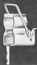
Fig. 365. The locking type component holder gives a positive grip. The large
surface area of the holder helps heat dissipation. (Atlas E-E Corp.)
Flea clips
A rather odd terminal is the "flea clip," so named because of its size. Designed especially for mounting subminiature tubes having co-planar leads, the flea contact is shown in Fig. 362. It is made from beryllium copper and then silver-plated. Mounting is accomplished by pressing the clip into a 1/16-inch-diameter hole. The lower end of the clip has a tapered hole which will take up to 1/32-inch-diameter wires, and the entire assembly can be soldered, if required, for permanent tube lead mounting. Where tighter fits are needed in production work, the clip is mounted in .050-inch square holes punched out of the base stock with a die.
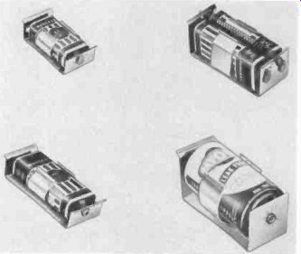
Fig. 366. Various types of battery holders. (Austin Co.)
Component holders
Another important class of subminiature and printed-circuit hardware is the component holder. These have been manufactured to hold everything from an electrolytic capacitor to a subminiature diode. A common type, the spring clip, is shown in Fig. 363.
Vertical holders ( Fig. 364) permit component mounting in limited spaces, especially where part of the tube envelope can be kept below the plane of the base board or chassis. Another component holder is the locking type shown in Fig. 365. This gives a more positive grip and increased contact pressure which helps to reduce heating of the component being held. Clips are also avail able with integral soldering lugs where grounds or common tie points are required.
Battery holders
Fig. 366 shows a few battery holders designed to make battery replacement easier. Numerous constructions are available, including dimpled ends, spring retainers, insulated and noninsulated bodies, and series-parallel combinations.
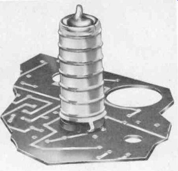
Fig. 367. Metal shield designed specifically for printed-circuit use. (Slaver
Co.)
The usual construction material is aluminum. Sizes available range from single penlite cells to holders for as many as four size-D flashlight cells. Models are made for mercury cells as well as ordinary carbon types.
Shields and heat sinks
Heat, vibration and electrical interference have always been enemies of electronic circuitry, and several ingenious designs have been produced to minimize the effects of these elements on vacuum tubes used in subminiaturization and printed-circuit work One form of shield for printed-circuit boards is shown in Fig. 367. A modification of a standard miniature shield, it has a flared bottom to allow the shield to fit over the ground lug of the printed-circuit socket and provide contact from shield to circuit ground. A vertical seam makes up for minor variations in tube diameters. The materials used for construction are tinned steel and aluminum. A subminiature shield clamp is shown in Fig. 368.
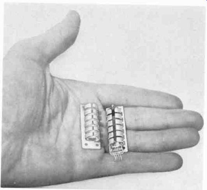
Fig. 368. Shield clamp used with subminiature tubes.
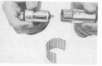
Fig. 369. A corrugated shield insert is often used to help reduce tube temperature.
(Birtcher Co.)
Shown in Fig. 369 is a corrugated shield insert designed to reduce miniature-tube temperature and prolong tube life. The device is made of .003-inch-thick spring brass with a dull black finish. The corrugated strip is cut to the proper length and formed into a cylinder which is then fitted between the tube and a conventional shield. The corrugations touch both tube envelope and shield, providing heat transfer to the shield and shield base. The corrugated shield inserts come in several sizes to fit T-5 1/2 and T-6 1/2 tube envelopes. Other forms are available for the sub miniature T-3 series.
Fig. 370. Extremely small jacks and plugs are needed for compact circuitry.
Individual plugs and jacks
A few of the smaller plugs and jacks adaptable to printed circuits and subminiature use are shown in Fig. 370. The principal points to keep in mind when choosing this type of component is the ease of connecting and disconnecting, and the contact resistance of the combination. Insulating materials vary from nylon to phenolics, depending on voltage breakdown ratings. Contact springs are ordinarily beryllium copper, brass or phosphor bronze. Both open, closed and combination jack circuitry is available.
Electro-acoustic devices
An important class of components used as input-output transducers are microphones, earphones and speakers. Converting sound pressure into modulated electrical voltages and currents, these components have also shrunk to accommodate printed-circuit and subminiature requirements. Typical miniature micro phones and speakers are shown in Figs. 371 and 372.
Subminiature tubes
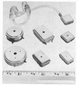
Fig. 372. A variety of "flat" earphones made primarily for hearing
aids. (Courtesy Knowles Electronics.)
Despite the advent of transistors, certain factors such as standardization in manufacture, power ability at higher frequencies, lower first cost on many types of tubes, and availability of multipurpose types in one envelope still weigh heavily in favor of continued use of subminiature tubes.
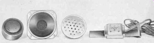
Fig. 371. Typical miniature microphones and speakers.
Subminiature tubes are generally of two types-the round envelope and the flat press. Both are shown in Fig. 373, compared to a conventional seven-pin miniature tube.
Considering the size of these tubes, it is almost a miracle that they can be made, not only to work, but also to be fairly consistent in overall performance. Among the manufacturing problems involved are holding dimensions in the spacing between elements, life expectancies and envelope sealing. Sealing techniques employ special gas atmospheres and tooling. The part carrying the electrode pins, called the mount, is sometimes assembled separately and then set up in special supports. Then the glass envelope is pressed around the mount. The electrodes are also premounted in certain methods of manufacture in a "button" made of glass. This button, in turn, is joined to the tube envelope in later steps of the tube-making operation.
Common filament materials are tungsten wire and nickel alloys.
Cathodes are generally coated with metallic oxides. Carbonized nickel is used by several manufacturers for anodes.
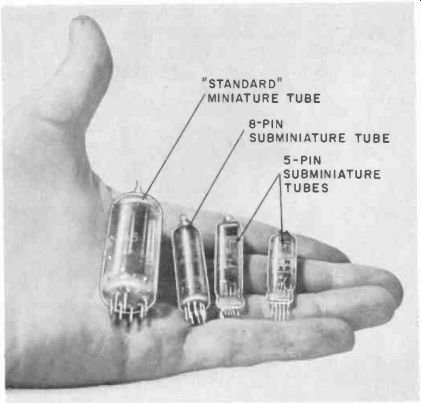
Fig. 373. Round envelope and flat-type subminiature tubes. Note their relative
sizes as compared to a standard 7-pin miniature tube.
Cautions in use
With small size, the technician must expect to accept a few problems. Among the bugs present in subminiature tubes are microphonics, poor heat-life ratings, mounting considerations, shielding methods, and the concept of "reliability." Microphonics are the spurious electrical outputs caused by conditions such as vibration, shock or other mechanical forces. The manufacturer tries to overcome this problem with more rigid electrode assemblies, and by relocating electrodes to give the least spurious outputs with external disturbances.
Heat dissipation is a very common problem in subminiature assemblies where component density is high and there are many tubes in the circuit. One method of reducing heat on. the tube is shown in Fig. 374; a shield-base-plate combination conducts the heat away from the tubes and radiates it to the air. Excess heat and elevated temperatures also electrolyze the tube leads and they react with the glass in the envelope. Heat will also cause gas to be driven from the tube walls and internal elements of the tube, reducing the life expectancy of the tube.
"Reliability" is a measure of confidence in the use of the tube.
Will a certain tube always give a certain number of hours of life under a certain set of conditions? Of, say, 100 tubes, how many will fail after so many hours of use? These are only two of the ...

Fig. 374. The combination shield-baseplate
helps keep the tube cool.
... questions that "reliability" studies attempt to answer. The tube manufacturer is constantly caught in a maze of compromises to achieve dependable performances. In general, two things can happen to affect tube life adversely. The first is that manufacturing know-how can be at fault and the second is that the user can misapply the tube, putting it into a circuit for which it was never designed. The average tube manufacturer employs 10 to 20 tests on a single tube to insure a minimum standard of performance. In the case of the so-called "reliable" or "premium" tubes, the tests often number up to 50. The state of the subminiature tube art has reached the point where a 1,000-hour guarantee is common and 5,000-hour guarantee on the "reliable" types are becoming standard.
Testing sub-miniature tubes
The most frequent complaint with these tubes is an open filament. This is not surprising since many subminiature tubes operate at A-voltages of 1.5 or less, and sudden surges or accidental shorts in the filament circuits can be fatal. Filament continuity can be checked with an ohmmeter using one of the higher ranges such as 100,000 ohms or 1 megohm full scale. This is a precaution to prevent the ohmmeter battery from burning out the low-voltage filaments. In making such a check, remember that high-loss dielectric surfaces can indicate false shorts due to leakage resistance, so the ohmmeter probes should not be allowed to come in contact with plastic tabletops or plastic chassis.
Subminiature semiconductor devices
Transistor theory and operation have been covered much more thoroughly in many other books, and only the highlights of transistor techniques as affected by printed circuitry and subminiaturization will be dealt with here. The transistor consists of a wafer of semiconductor material--either germanium or silicon--to which three external leads are attached. Fig. 375. A number of small component mounting clips are designed for holding transistors to a chasm.
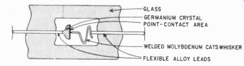
Fig. 376. Internal construction of a germanium diode. (Hughes Electronics)
Depending on the manufacturer and the particular design, the assembly is encased in metal or glass.
In contrast to its minuteness, it is a very rugged component mechanically, especially under shock and vibration. However, transistors are very susceptible to electrical and heat damage.
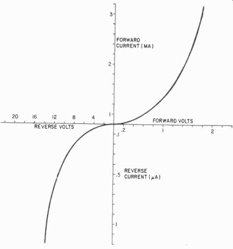
Fig. 377. Characteristic curve of a semiconductor diode shows that it will
pass more current in the forward than in the reverse direction.
When handling transistors check and double-check manufacturer's data on the unit. Polarities with respect to batteries must be watched closely; the so-called n-p-n types are not directly interchangeable with the p-n-p on this account. Whenever possible, meters should be used to monitor circuit currents. One potential danger to transistors, overlooked many times, is using a high-level output from a signal generator to troubleshoot. Do not use a low-range setting on an ohmmeter because of the applied voltage which might damage the transistor.
Mounting transistors
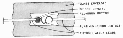
Fig. 378. Internal construction of a silicon diode. (Hughes Electronics)
Transistors can either be soldered in or put in sockets. If the transistor is soldered into the circuit, a heat sink must be used during soldering. Also use as much of the pigtail as possible and try to keep the heated point as far from the body as you can.
Fig. 379. A typical midget selenium photodiode.
Clipping a small alligator clip on the lead during soldering helps dissipate some of the heat that would normally be conducted to the transistor body. Do not twist the leads or bend them too much in installation. They will withstand a few gradual 90° bends, but will not take repeated sharp bends without breaking off. Several small component mounting clips are made to hold transistors on a chassis. These are shown in Fig. 375.
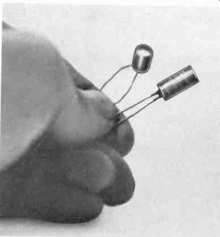
Fig. 380. Cadmium selenide photodiodes.
Testing transistors
Transistors can be tested by substitution or by instruments. The substitution method is more reliable. When checking transistors in place on a chassis, be careful with any sort of test prods. Printed circuit connections and associated subminiature components are packed in tightly and it is very easy to short-circuit a few terminals with the prod. Accidental shorts can produce enough current to ruin the transistor and, quite often, a few other components.
Diodes
Fig. 381. Germanium photocell. This type of unit can provide power for small
radios when a number of the cells are used. (International Rectifier Corp.)
It is difficult for the average user to determine if transistors or diodes are more important and also which of the two components are in wider use. Often mistaken for 1/4-watt carbon-composition resistors at first glance, the diode performs all sorts of tasks from simple rectification to FM detection. A major field of use is computers where, in conjunction with small magnetic "memory cores," the diodes provide decision-making and information storage in incredibly small packages.
The bulk of diodes manufactured today are encased in glass envelopes which seal the semiconductor materials from the atmosphere and act as a rigid support at the same time. The wire leads and the glass envelope are made so that they have as near equal temperature coefficients of expansion as possible to insure against cracking. The semiconductor material is mounted at the end of one of the leads, and a cat's whisker electrode is mounted at the end of the other lead. Various color codes and symbols are used to indicate polarity of the diode. Typical construction is shown in Fig. 376. The average size of such diodes is about 1/8 to 3/32 inch in diameter by 1/4 to 3/8 inch long, the leads being anywhere from 1-1/2 to 2 inches. The glass is often coated with an opaque material to cut down effects of light, since many semi conductors are photosensitive.
Basic rectifier characteristics are shown in Fig. 377. The curve simply says that in one direction the diode will conduct more than in the opposite direction. Another way of looking at it is that the unit has a high backward resistance and a low forward resistance.
For applications where plain rectification is needed, the user is not concerned too much with a property called recovery time.
However, in certain cases, such as computers, the so-called recovery characteristics are very important. This ability of the diode to reach a certain current value or voltage drop in a certain time is tested by applying a current or voltage pulse. Recovery time is measured in both forward and reverse directions.
Diodes, like other semiconductor devices, are very sensitive to temperature extremes. When soldering, some heat sink such as pliers or an alligator clip should be inserted between the diode body and the soldered point.
Spot-welding techniques can be used to apply concentrated heat for very small periods of time.
Silicon diodes, a newer development, permit operation at higher temperatures than germanium and, as a result, also give more power-handling ability than germanium units at lower corresponding temperatures. Normal ranges of germanium diodes run from 60° to 180°F, whereas silicon units operate as high as 270°F. Silicon is a very brittle material, and some silicon diode designs make provision for this property. In the unit shown in Fig. 378, a spring and soft metal mounting button are used to overcome breakage due to sudden shocks and thermal expansion.
Subminiature photoelectric devices
The major materials used at present for small photosensitive elements are the semiconductors, germanium and selenium, and compounds of cadmium with sulfur and selenium. A representative midget selenium photodiode is shown in Fig. 379. About 1/10 inch in diameter and under 1 inch long, it has found use in punched tape reading, scanning and photographic exposure-metering devices. This photodiode has a small, polished germanium slab mounted in a molded plastic body. A tungsten whisker comes up to the slab, and the whisker is bent to bear down on one point of the germanium surface. Leads about 1/32 inch in diameter are brought out from the slab and whisker, through the body, and are color-coded. Illuminating the germanium slab causes its resistance to change. Current will increase with an increase in light. The diode can also be used in modulation applications such as "sound on a light beam" since the frequency response is in the range of 10 to 50 khz.
The units shown in Fig. 380 have a cadmium selenide compound as the photosensitive material.
This type of photodiode is sensitive to gamma and X-rays as well as infra-red. Current for a given amount of light is dependent on the applied voltage.
Typical operating data are 400 microamps at 100 volts dc and 2 foot-candles, with a decrease to about 40 microamps under the same illumination and 10 volts dc. The diode produces a slight amount of current ( dark current) when in total darkness, and this is in the order of less than 1 microamp. Some versions of this diode have been built with light-to-dark current ratios of 10,000 to 1.
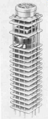
Fig. 382. A module is a vertically stacked array of components. The parallel
wafers are supported by wires known as risers. (Courtesy Aerovox Corp.)
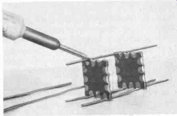
Fig. 383. Method of building a module using laminates and copper wires.
The germanium unit shown in Fig. 381 requires no external emf for excitation, and will produce up to 2 ma across a 10-ohm load.
A common experimental use is with a 0-1-ma meter as an exposure meter. The unit mounts on a bracket and is just under 1/2 inch wide by 3/4 inch high and 1/32 inch thick. Banks of these units may be series- and parallel-wired to drive small transistor receivers.
Modules and packaged circuits Many components are sometimes wrapped up in one package for ease in replacement.
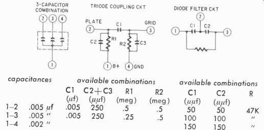
Fig. 384. "Packaged circuit" schematics are available in various
combinations. (Courtesy Sprague Electric Co.)
Some ceramic-based wax-coated units contain as many as two or three capacitors and a like number of resistors. Others include a three-capacitor combination, a diode filter circuit and a triode coupling circuit. Advanced forms of these ceramic-based units include audio output circuits and detector-pentode coupling circuits. Nine or 10 resistors and capacitors are common in the latter two circuits.
Repair of such packaged circuits is not practical, and ease of replacement and relatively low cost account for the growing use of such components.
A three-dimensional module (sometimes referred to as a Tinker toy) is shown in Fig. 382. The experimenter can duplicate some of these with laminate material and copper wire as shown in Fig. 383. Tinker toy modules are made commercially in the form of video limiters, cathode followers, multivibrators and dc regulators.
A third form of commercial module or packaged circuit is the unit shown in Fig. 384. The resistors are molded-composition types and the capacitors are tubular ceramics. Each resistor and capacitor is about 1/8 inch in diameter by 5/8 inch long, and
---- INVOICE
-00 Gernsback Library, Inc.
154 WEST 14th ST., NEW YORK 11, N. Y.
BILLS PAYABLE WITHIN 10 DAYS P L FOR SERVICING PRINTED CIRCUITS $3.35 KEEP THIS PART OF STUB FOR YOUR RECORDS (Cut Mom; Line) IND ARTS DEPT' EASTERN KY STATE COLLEGE RICHMOND KY SERVICING PRINTED CIRCUITS $3.35 IMPORTANT: PLEASE RETURN EXACT AMOUNT WITH THIS STUB
----
Fig. 387. A "pig-tailor" for measuring, bending and cutting component
leads. (Bruno- New York Industries)
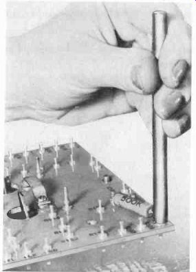
Fig. 388. A spin pin is used for wrapping component leads around turret-type
terminals. (Bruno- New York Industries)
Among the more advanced modules are the multistage sub miniature tube amplifiers.
Preparation of component leads
One of the methods used to prepare component leads for use in printed circuitry and subminiature work is "pig-tailoring." The amateur experimenter can duplicate this technique on a small scale by building a jig consisting of nails on a board. The component is then laid on the board and the leads bent to the desired con figuration and cut to length. These procedures are shown in Figs. 385 and 386.
A commercial machine has been developed to perform these operations in a very efficient manner. The machine, shown in Fig. 387, can be hand-operated, foot-operated or motorized, and is capable of simultaneously measuring, bending and cutting both axial leads of a component to accurate sizes and shapes. Only 2 to 3 minutes is required to make a specific lead-forming setup.
Any component 1-inch in diameter or less and 6 inches in overall length (including leads) or less can be "pig-tailored." Bends can be made as close as 1/16 inch to the body of the component. The unit occupies less than 1/3 square foot on the bench.
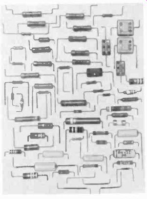
Fig. 389. Types of component lead shapes produced by pig-tailoring. (Bruno- New
York Industries)
The body of the axial lead component is placed between two guide supports which are free to move along a guide-support shaft. The component leads fall into notches of shearing and bending elements; one set of shearing and bending elements is used for each component lead. Depressing the main drive lever will move the shafts, which in turn actuate the shearing and bending elements. The direction that each shaft rotates is adjust able with drive links and, by changing drive link positions, S- or U-shaped leads can be produced. Adjustments are made with Allen type setscrews.
An added feature is the ejector mechanism which is part of the bending elements. The ejector fingers travel vertically between stationary and rotary members of the bending elements when the main drive shaft is actuated.
When the rotating blades of the bending elements are clear of the notches in the stationary blade of the bending element, the ejector fingers move up and carry the component leads out of the notches. The components fall forward into a receiving tray and the rejected ends are cast out side the immediate work area.
A slotted tool known as a spin pin is used to wrap the ends of the tailored component leads around turret-type terminals. This tool is a substitute for the needle-nose pliers normally used for such operations and requires less skill to produce acceptable wraps. The spinpin helps cut down broken leads and broken component bodies by allowing the operator to "feel" tautness in the lead as it is wrapped. Handling of the chassis or terminal board is cut down since the spinpin can be used in any place where it reaches. Another advantage is that the lead can be wrapped until no end is left, thus eliminating a clipping operation. The spinpin is shown in action in Fig. 388.
The variety of work produced by pig-tailoring is shown in Fig. 389. The components pictured are used for printed circuits, turret terminal assemblies, socket terminations and tie-point terminations. S- and U-shaped bends in two and three planes are possible.