HERE are many methods of producing "printed circuits," or what most people think of as circuits, without the reed for regular point-to-point wiring.
One is a simple technique in which the conductors are "painted' on the insulating material in a manner similar to ordinary house-painting.
Another depends upon spraying hot metal in the form of a "vapor" onto the insulating background. Still another produces circuits by electroplating or reverse-electroplating-material is actually "plated off" the insulator instead of on to it. Die stamping, in which a metallic wiring pattern is cut out of a solid-conductor background, has been used for making printed-circuit antennas. In addition to these more popular methods, auxiliary techniques such as potting or encapsulating allow the circuit to be cast into rigid molds for mechanical protection. Soldering techniques are also very important in the art of printed circuits because poor solder or poor flux can ruin an entire chassis.
Techniques such as metalizing require specialized equipment and are mentioned only as background information for the technician. Imprinted circuit inlays are close cousins to the foil techniques described in Section 5.
Painting
Painted printed circuits are easy to make on both an experimental and production scale.
Conductive materials such as copper, silver and carbon are ground into fine particles and dispersed in solvents. The resulting paints are then brushed or sprayed onto the objects to be coated. In some cases, the paints are air-drying and require no additional source of heat. In others, it is necessary to apply the paint to the "base" material and then fire the painted coating in a manner similar to pottery glazing.
One ounce of silver is enough to paint several square inches of conductive surface and can easily produce many multi-tube circuit chassis. The pigment for resistors is mainly carbon black, although colloidal graphite is also used. Flake graphite can be used for brush painting mixtures while carbon black and colloidal graphite are more adaptable to spraying and silk-screening. A binder-linseed oil, cottonseed oil, lacquers or silicate-holds the pigment together in the solvent.
Some forms of printed-circuit paints contain reducing agents, such as formaldehyde, which are used to convert the salts of the metal to the pure metal at low temperatures. Silver oxide and silver nitrate are two agents used to produce pure silver.
A solvent adjusts the viscosity of the paint. Some of the more common ones are acetone, various alcohols, ethyl acetate and amyl acetate. Sometimes solvents which attack the base material are used to improve adhesion of the conductive coating to the base; for example, toluene on polystyrene. Toluene, a relative of benzene, "etches" the surface of the polystyrene and allows the silver or other paint to obtain a firm grip on the base.
Some typical silver and carbon paint formulas are given in Tables 2-1 and 2-2.
-----------------------
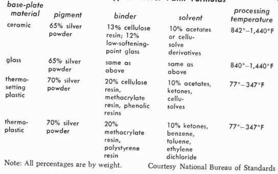
Table 2-1. Typical Silver Paint Formulas
base-plate processing material pigment binder solvent temperature ceramic 65% silver 13% cellulose 10% acetates 842°-1,440°F powder resin; 12% or cellu low-softening- solve point glass derivatives glass 65°k silver same as same as 840°-1,440°F powder above, above thermo- 70% silver 20% cellulose 10% acetates, 77°-347°F setting powder resin, ketones, plastic methacrylate cellu resin, phenolic solves resins thermo- 70% silver 20% 10% ketones, 77°-347°F plastic powder methacrylate benzene, resin, toluene, polystyrene ethylene resin dichloride
Note: All percentages are by weight. Courtesy National Bureau of Standards
----------------------------
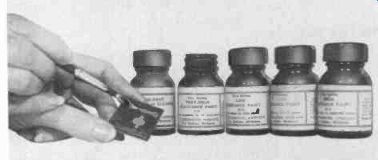
Fig. 201. Painting a printed circuit. (Courtesy Micro-Circuits Co.)
Surface preparation for painted circuits
The insulated surface on which the conductive paint is laid down has to be prepared in many cases. In the case of plastic bases such as Lucite or Plexiglas, a light sanding with fine sandpaper ( 180 grit) will do the job. The unpainted parts of the base material must be protected with heavy masking tape. Glass surfaces can be etched with commercial etching pastes such as Etchall or else hydrofluoric acid can be used. When using hydrofluoric acid, protect your eyes and hands from the acid fumes.
After roughening the surface, scrub it perfectly clean. Dirt will weaken the bonding between the paint and the base material.
--------------------
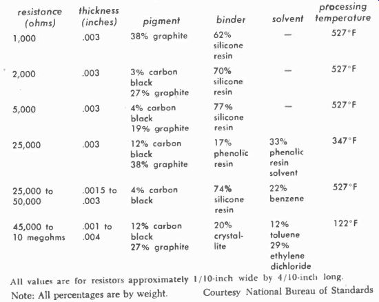
Table 2-2. Typical Carbon Paint Formulas
resistance thickness processing (ohms) (inches) pigment binder solvent temperature 1,000 .003 38°. graphite 62% silicone resin 527 F 2,000 .003 3% carbon black 27% graphite 70% silicone resin
- 527 F 5,000 .003 4% carbon black 19% graphite 77% silicone resin
- 527 F 25,000 .003 12% carbon black 38% graphite 17°.
phenolic resin 33°.
phenolic resin solvent 347 F 25,000 to .0015 to 4% carbon 74°. 22°. 527°F 50,000 .003 black silicone resin benzene 45,000 to .001 to 12% carbon 20°0 12% 122°F 10 megohms .004 black 27% graphite crystallite toluene 29% ethylene dichloride
All values are for resistors approximately 1/10-inch wide by 4/10-inch long.
Note: All percentages are by weight. Courtesy National Bureau of Standards
---------------------------
Ordinary detergents work very well in this respect, but they should be followed with several water rinses.
Putting on the paints
The painting of printed circuits is shown in Fig. 201. Brushing is the commonest method for small-lot runs; an ordinary camel's hair or sable brush can be utilized. Use even strokes and take care to avoid air bubbles and excessive paint buildup. Stir the paint occasionally to prevent settling or thickening. Adjust paint viscosity by thinning with solvent or else allowing the paint to evaporate, depending on the results desired.
Stencil techniques can also be used, and stencils prepared as described later in this section will hold up for several dozen or even several hundred runs. Another method for applying the inks or paints is to use an ordinary printing press. The ink plate of the press is coated with conductive or resistive paint. The pattern of the electronic circuit is made up as a form of "type" and put into the press where the regular type is usually set. The base material to be printed is laid on the plate where the paper usually goes, and the press is then operated.
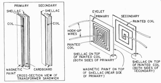
Fig. 202. Construction details of a printed-circuit transformer.
Repeated printings will build up the coating thickness, giving a wide variety of conductance or resistance values. Silk-screen techniques can be used very success fully for large production runs when tolerances have to be held more closely than can be done with hand-painting methods.
Conductive and resistive paints
The most common use for these materials is to paint conductive circuit lines on an electronic circuit board. Some of the less obvious uses include:
1. Measuring a break or tear in a surface by coating the surface with conductive paints and stretching or abrading the surface while the coating is in series with an ohmmeter.
2. Strain-gauge devices for weighing various objects. A layer of conductive paint acts like a varying resistance when the coated member is stressed, and the relation between stress and resistance can often be found experimentally.
3. Moisture-detection devices similar to the rain-gauge detector described in a subsequent section.
4. A substitute for a broken metallic part or a working model of a complex metallic part. By shaping the part from wood or plastic and then coating it with conductive paint, it is possible to make a very inexpensive model. Dipole antennas have been made this way, using wooden dowels coated with conductive silver paint.
5. Measurement of surface and volume resistance. Small dots or lines of conductive paint can be used as electrodes for point-to point volume and area resistance measurements.
6. Silver conductive paints have been used for electromagnetic and electrostatic shields in TV tubes. These paints have also been used to dissipate static which builds up on windshields and phono graph pickups.
7. By painting carbon resistances around a glass beaker, the resulting element can be used to boil water in the beaker or else heat water to a given temperature, using a thermostat to control the resistance-paint heater. The section on components has de sign information for computing the wattage of resistors using painted-circuit materials.
8. By coating a vibrating object with conductive paint and making it part of a capacitor, the vibration of the object can be measured as a function of capacitance changes.
9. Areas of conductive paint are brushed on box tops and other moving objects so that when the box or object passes certain points on an assembly line, solenoids triggered off by the coatings kick the objects to one side or perform predetermined operations on the boxes. These paints can be put on coded wheels and used as programming timers.
Magnetic paints and pastes
Miniature transformers can be made by using magnetic paints and pastes composed of metallic pigments dissolved in binders.
These pigments are mainly iron-base materials and can be applied over coils and wires to increase inductance and coupling and also to control magnetic leakage. A transformer can be made as shown in Fig. 202 by placing one coil on each side of the base material and building up with alternate layers of shellac, like laminations in a regular transformer.
A thermoplastic version of these magnetic materials is available for casting special core shapes.
Spraying or metalizing Although the metalizing process has been used since 1935 by electrical manufacturers, it has been applied to printed-circuit work only since the mid-1940's.
The basic idea of the process is to spray molten metal onto a base plate, using a stencil to produce the desired pattern. The process is too complicated for the average experimenter.
Imprinted-circuit inlays
The main feature of this technique is that all of the circuit conductors are cut out of a solid sheet of copper or silver and then attached to the base material by fusing with heat. Dies are used to cut out the conductor pattern, two dies being required for a circuit having a pattern on both sides of the insulator base.
The dies are mounted in a heated embossing press, and the time and temperature of pressing controlled closely for proper operating results. Practical methods using brass shim stock for making switches are given in section 6.
Spray milling
The most famous application of this technique was in the Sargrove broadcast receiver (Section 1 ). The spray-milling process was a technique conceived for mass production of small ac-operated broadcast receivers.
Two plastic base panels with preformed holes and indentations were fed into automatic machines in which the panels were sand-blasted and then sprayed with zinc. The excess wire was then milled so that the remaining zinc formed wires, capacitors and inductors in the depressions. At another stage, carbon (graphite-dispersion) resistors were sprayed on through stencils, and hardware, such as the tube and electrolytic capacitor sockets, was put on. The units were tested automatically and coated with protective resins to keep out dirt and moisture. The circuit wiring and spray-milled components were determined by whatever grooves were molded in the base panels. Inductors were formed by spirals, and capacitors by leaving thin grids in the. panels during fabrication and spraying metal on each side of a grid to form a dielectric combination.
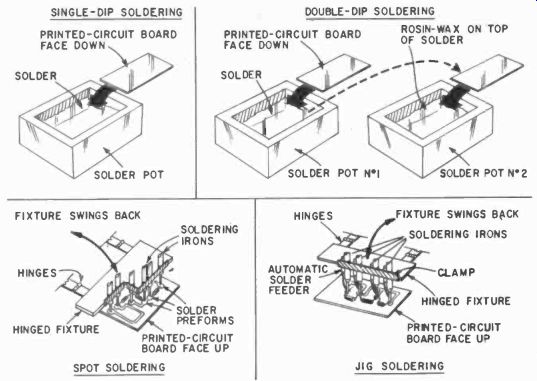
Fig. 203. Dip-, spot- and jig-soldering methods----SINGLE-DIP SOLDERING DOUBLE-DID
SOLDERING
Stamped wiring
The basic idea in the die-stamping printed-circuit technique is to form a series of bus bars on an insulating base and then proceed to interconnect these bus bars to produce a circuit.
One variation is to run one set of bus-bar conductors horizon tally on one side of the base board and to run the other set of bus-bars on the other side at right angles to the first set. Crossovers are made by simply putting eyelets or pins through the right junctions. Another technique is to have holes and slots punched or drilled in the base panel before the stamped wiring is inserted.
In this method, the stamped wiring can be attached by spot welding or resistance-soldering methods, eliminating eyelets. For single connections on one side of the board, eyelets or pins can be put through at some point which will not connect to any metal conductor on the opposite side. The stamped-wiring technique is limited mainly to low-voltage low-current applications, but has the distinct advantage of corresponding very closely to electronic equipment schematic diagrams.
Instructions for making stamped wiring devices are given in Section 6. The experimenter can duplicate some simple yet practical circuits with only a scissors, some copper foil and a few eyelets or rivets.
Stamped wiring is slowly losing favor to the more modern etching methods.
Encapsulation and potting
Encapsulation and potting techniques are relatives of the ancient art of casting parts in metal boxes and pouring pitch over them-a practice reminiscent of old-time radio days. The potting materials keep out dirt and moisture while offering mechanical support.
The worker has a large variety of materials from which to choose in these techniques, which are auxiliaries to printed-circuit and subminiature package production. A practical setup is given in Section 6.
Soldering methods
Although conventional soldering-iron techniques would appear suitable enough for printed-circuit work, refinements have been developed. For one thing, cold solder and rosin joints would be more likely to occur in hand-soldering methods and, second, the hand-soldering operation would slow the speed at which printed circuit boards could be produced. The major soldering techniques are the single-and multiple-dip and jig-soldering systems. however, as important as the actual soldering methods used is the choice of a solder and a flux.
Dip-soldering technique
There are two main kinds of dip soldering-single and double dipping.
In the single-dip method, the circuit board is first fluxed with a 50-50 mixture of alcohol rosin flux. The flux can be "painted" on or else the board can be "dunked" in a tray containing the flux mixture. When the board is completely fluxed, it is dipped into a solder bath at about 450°F. The board must be moved back and forth during the dip. After about 5 seconds, the board is taken out of the solder by withdrawing one edge first and using that edge as a pivot.
Double-dip soldering uses two solder pots and is about the same as single-dip except that the second pot contains a rosin-wax mixture which floats on the surface of the soldering bath. The wax provides moisture and fungus protection.
Spot and jig soldering In spot soldering, soldering pre-forms ( bits of solder made up in advance in different shapes) are placed at various points on the printed-circuit board. A fixture which holds one or more soldering irons is then brought down on the work. Jig soldering is a variation in which self-feeding irons are brought down on the board.
Dip, spot and jig-soldering methods are shown in Fig. 203.
They are mainly for advanced workers and commercial use. The spot-soldering method, using pre-forms, can often be used in printed-circuit repairs.
Solder masking techniques
It is usually necessary in all forms of dip soldering to mask certain areas of the base conductor pattern to prevent the adherence of solder. This is true, for instance, where mechanical tolerances must be held for component mounting. It is also better to mask as much as possible of the conductor base not needed for actual soldering. This prevents solder bridging due to large bare-copper areas.
One of the easiest masking methods is to apply high-tempera ture masking tape to the areas which require protection; the tape is stripped after soldering.
Masks can be made from good insulators such as asbestos or mica-and attached to the circuit panel before dipping. There are also solder-resistant paints or lacquers that can be applied by brush or stencil methods and which will shed the solder during the dip. These materials usually require baking, however, since they are thermosetting compounds.
Soldering troubles
In addition to the difficulties experienced in the soldering end of the operation, there are several troubles associated with the solder pot itself. Quite frequently, there is metallic contamination of the solder due to the solvent action of the molten solder on the work being dipped. The solvent action is really part of the soldering reaction and is perfectly normal. Where copper and zinc base alloys are used, there is rapid contamination of the solder bath because the copper and zinc dissolve easily in the molten solder.
In the case of solder baths and pots, the best thing to do when the solder shows signs of becoming "slushy" and hard to work with is to replace it with fresh solder. Do not attempt to adjust the bath with random additions of pure tin or small amounts of fresh solder.
The temperature of the solder bath is important. Too high a temperature promotes blistering of the board as well as formation of ' dross" on the solder's surface. Too low a temperature increases soldering time and the possibility of getting cold joints.
The pot should be large enough so that introduction of the printed-circuit board will not drop the pot temperature.
Surface dross and oxides are an ever-present problem, and the use of a so-called "cover flux" is not recommended since these contain chloride salts. These volatile compounds generate annoying fumes and create corrosive residues. An occasional skimming of the solder pot with a steel or ceramic blade is preferred by most workers.
Solder characteristics
Remember that soldering is an alloying operation and that a solder has varying characteristics.
Some of these are the way the solder spreads, the speed at which the alloy is formed between solder and object being soldered, the resistance of the joint to mechanical stresses and shocks, the porosity of the joint and its chemical resistance. Avoid impurities such as zinc and aluminum when choosing a solder since they form rough, porous joints. The most popular solders are the 50-50 and 63% tin-37% lead mixtures.
This 63-37 mixture is sometimes called a "eutectic." This simply means it is the lowest-melting-point combination of tin and lead for practical uses. Silver solders used in printed-circuit work are tin-lead alloys with small amounts of silver added. They can be used when repairing silver-plated or silver-fired ceramic circuits.
Flux considerations
One of the popular fluxes for soldering is rosin, which owes its fluxing activity to a chemical compound called abietic acid. Since the amount of this acid varies, depending on whether the rosin is from wood or from gums, the activity of the different rosins will vary. In choosing rosin flux for printed-circuit use, bear the following factors in mind: its ability to speed soldering, the amount of heat necessary to melt or activate it, whether it tends to boil or spatter, the forms in which it can be applied, its leakage resistance as it lays on the printed-circuit pattern, and its corrosiveness.
A novel idea is the use of a flux containing a dye. It can be used to indicate soldered joints that need resoldering, at the same time providing the necessary flux. It is also helpful at printed-circuit inspection points in a production line.
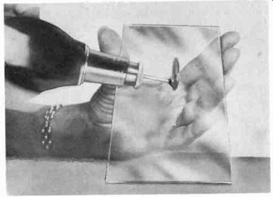
Fig. 204. Special technique for soldering on glass.
Special soldering techniques
Occasionally it is necessary to solder a glass or ceramic component to a metallic one. One particular case might be the use of ceramic or glass tubing as a high-frequency coil form. It might also be necessary to solder to aluminum or stainless steel, using ordinary 50-50 tin-lead solders.
A special technique' is shown in Fig. 204. A small hand grinder is fitted with an abrasive wheel, and the wheel is brought to bear against a bar of soft solder. The solder will eventually melt and flow onto the surface of the wheel, actually "loading' the pores of the abrasive with solder. The rotating solder-laden wheel is then brought up against the work surface to be soldered, and slight pressure applied. The friction created melts the solder, and it flows onto the surface of the work, now abraded by the grinding action of the wheel.
[Developed by Joseph McGuire of Los Alamos Laboratories.]
After this preliminary "tinning" operation, soldering can be done in the regular way, using 50-50 solder. A little practice is required not to heat the base material too much. An alloy called Wood's metal, available from druggists and chemical supply houses, works very well with glass and ceramic materials. Do not depend on the joint for great mechanical strength, but mainly for electrical connections. High grinder speeds tend to oxidize the solder, but the proper speed will put down a shiny solder coating in a few minutes or less.
Indium-based solders for glass to metals
Solders composed of indium metal and tin have the property of "wetting" glass, mica, quartz and thermosetting plastics. These solders melt in the range of 250°F and are applied by melting in a crucible and swabbing onto the work with a cotton applicator or cheesecloth. The work must be warmed to the solder melting temperature for best results. If the work is too hot, the solder will not adhere. No flux is required in using these solders, but the glass or ceramic must be scrupulously clean.
Etched circuits
Without a doubt, the best known and most widely produced printed circuits are the so-called etched circuits. A resist is laid down on the laminate material and, by various selective methods, the conductor pattern is caused to appear in the foil. The techniques for laying down the resisting agent and the etching differ widely and can be divided into two broad major classes-mechanical and photographic.
Photographic etch-resist methods
These will be treated first, since they constitute the most popular methods used today. They consist of putting some photo sensitive material on foil, after which the sensitized foil is exposed in a conventional manner and then developed. The foil is coated with a photosensitive emulsion which changes its solubility after being exposed to strong actinic ( ultra-violet) light. After development, the resist is exposed to light, hardens, and the non-exposed resist washes away to leave bare base-metal foil on the laminate. The final step is etching with ferric chloride or chromic acid.
[A commercial trade name for such a solder is Cerroseal ( Cerro de Pasco Co.). One such commercial method is the Kodak photo-resist system.]
Many precautions must be observed if this material is to yield good results. In the first place, all materials which contact the resist after sensitization must be dry. It is a fundamental property of the resist to harden upon contact with water. In addition, the photo-resist material should be handled in a dim light, preferably a 10-watt amber lamp. Although a darkroom is not necessary, light tends to decrease the activity of the chemicals.
Clean the copper or metal laminate thoroughly with a cleansing powder such as kitchen cleanser, before sensitizing. After the laminate has been cleaned, handle the plate only by its edges or with a wire handle hooked through a hole in one edge of the laminate. Oil and dirt from the fingers will cause smudging and spotting. The cleanser scouring should be followed with a hot water rinse, allowing the plate to dry by evaporation.
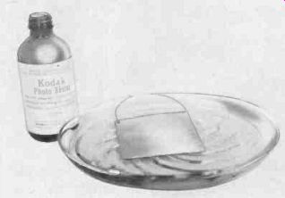
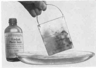
Fig. 205. (above). Dipping the laminate into photo-resist to sensitize it.
(below) Removing the laminate by a wire handle attached for this purpose. (Courtesy
Eastman Kodak Co.)
Pour the photo-resist into a glass tray and dip the laminate panel face up (Fig. 205) to insure a uniform spread of the photoresist over the metal foil surface. The panel should then be hung up by a parallel edge-not diagonally as in film--negative drying--to avoid streaking across the plate. The sensitized laminate should be dried in a dust-free room; it will dry in an hour or so without the addition of extra heat. If several laminate panels are sensitized at one time, be sure to store the extra panels after drying in dark, moistureproof paper, away from light.
Fig. 206. This negative is used to impress the pattern on the sensitized laminate.
A negative ( Fig. 206) is made by one of the methods described in later sections and the sensitized laminate foil and negative are 74E ...
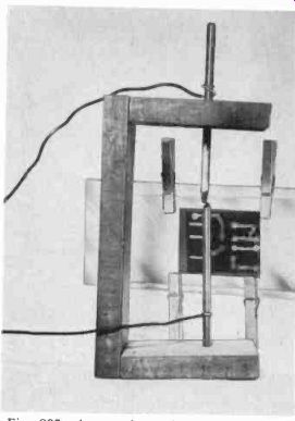
Fig. 207. An arc lamp is used to expose the laminate.
... exposed as shown in Fig. 207. A photoflood lamp can be used, but a mercury-vapor ultra-violet light or an arc lamp is better. For best results, use the special ultra-violet lights made for photographic purposes. The negative or stencil should be in good con tact with the sensitized material at all points. Exposure time is a matter of experiment: a rough rule of thumb is about 5 minutes with a Sperti No. 105 lamp at about 2 feet. A wise procedure is to use small pieces of sensitized foil as "test strips,' as in contact photo-printing methods.
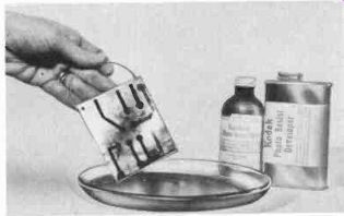
Fig. 208. Developing the exposed laminate plate.
The exposed image must be developed immediately in photoresist developer, which can also be set out in a glass tray. Development takes about 2 to 3 minutes. Agitate the plate constantly during development. It is another peculiarity of this process that the developed image does not show up very visibly, even though the developing agent washes away the resist which was not hardened by the action of the ultra-violet light. Although it is not absolutely necessary to see the pattern, one good way to bring it out is to use photo-resist dye. After removing the developed plate from the developer, transfer it directly to the dye ( Fig. 208) and submerge for about 1 minute without wetting the image with water. After dyeing, wash the image under a gentle stream of lukewarm water. The dye will leave the light-struck areas showing as dark black lines, and the light-protected areas will show through as the base laminate foil. The wiring shows as the black pattern and can readily be checked against the schematic or master drawing. The foil is then etched as described in the section on etching.
Manufactured by the Pennacel-LePage Co.
Glue-type photosensitive resists
Fig. 209. A phono-turntable setup for whirling the plate when using the Permacel-Lepage
glue-resist technique.
Fig. 210. Exposing the sensitized plate to an arc lamp.
For those who do not have time or facilities for compounding their own sensitizers, a photosensitive liquid is available for the job.' This material is an organic colloid, light brown to straw in color, depending on whether it is wet or dry. It is syrupy, but can be thinned with water. Although the technique described here is for a copper laminate, the same method can be used to set up resist patterns on monel, aluminum and steel.
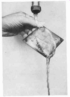
Fig. 211. Developing the exposed plate.
The first step in making printed circuits with this material is to clean the laminate board with pumice or rottenstone. The board is then rinsed with tepid running water. A uniform film of water will indicate a good, clean foil. Drain the excess water off and apply the resist. It can be brushed on or whirled on as shown in Fig. 209, using a deep circular pan attached to a phonograph turntable. The resist can be diluted with water prior to use.
Some experimenting is necessary to determine the best consistency for either painting or whirling. An infra-red lamp is used to dry the resist during the whirling process, or the material can be dried naturally if desired. One or two coats are used, depending on the thickness required to give satisfactory results.
After coating the laminate foil plate, the negative of the circuit pattern and the sensitized plate are put together in a printing frame and exposed to an arc light ( Fig. 210 ). A rough rule of thumb is to measure the diagonal distance across the frame, and hold the frame at half this distance from the arc if it is a single carbon arc. Printing time varies from 8 to 10 minutes. If the frame becomes too warm, cool it with a small fan.
Develop the exposed laminate foil plate under running water at about 110°F, as shown in Fig. 211. The water should not hit the exposed plate too hard. Swab the emulsion on the plate lightly with a cotton swab during development.
After developing the image, the colloid material is burned in under the heat lamp or in an oven. This drives off excess moisture and toughens the image for handling. The last step is immersion in an 'etchant such as ferric chloride or ammonium persulfate.
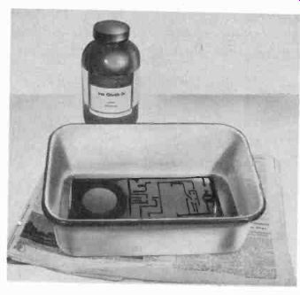
Fig. 212. Etching the laminate. Note that an enameled pan is used because
of the corrosive nature of ferric chloride.
The basic principle of the process is that dark areas in the negative protect the sensitized photo-colloid surface from exposure, and the lighter areas permit exposure. Exposed areas become insoluble and remain after development as the resist.
After etching, the remaining colloid is removed by careful application of dilute (5%) caustic-soda solution or by gently scraping the colloid layer with a knife or very fine sandpaper.
Etching the home-made plate
While etching methods will be detailed more fully later, a simple procedure is outlined here for the home-made circuit pattern. A ferric chloride solution ( Fig. 212) is used to etch the un wanted sections of the foil pattern. Use rubber gloves when handling this material, since it is very corrosive. Ferric chloride usually comes in lump form and can be obtained at a drugstore or chemical supply house. An average working solution can be made by dissolving 4 to 6 ounces of lump chloride in a pint of water. Increasing the concentration of chemical and heating the solution during etching will increase the etching rate. The etchant should be handled in a glass or enamel dish. Follow carefully the precautions given in the section on etchants.
After etching, remove the hardened sensitized "emulsion" with household cleanser or by brushing very gently with steel wool.
The board is now ready for fabricating operations such as drilling, plating, soldering and mechanical component mounting.
The experimenter may prefer to try other mediums in a home-made "emulsion." Some of the others that have been used are animal glues, egg albumen, casein glues and special grades of gelatin. A photoengraving concern can suggest specialized glues and formulas for making photosensitive "emulsions" which are more refined. Several commercial photosensitizing glues in tubes are on the market, ready to apply.
Etchants Among the etchants in wide use are nitric and chromic acids and ferric chloride. Nitric acid is a very rapid etchant; however, it gives off poisonous fumes and it is hard to achieve uniformity in small-lots. The tendency for nitric acid to be a violent etcher that is, to throw off large amounts of gas bubbles-makes it useful with a limited number of etch-resisting materials. Nitric acid offers the advantage of being capable of regeneration, and the copper can be recovered as copper nitrate. Both of these operations can be performed on a continuous basis, making the acid suitable for some forms of commercial work.
Ferric chloride is a more popular etchant and offers good uniformity in etching for small as well as large amounts of work. It is also readily available from chemical supply houses. The commercial or technical grade is best for printed circuits. Ferric chloride does not produce fumes, a decided advantage. About 43% by weight of ferric chloride will dissolve a little over 1% ounces of copper for every pound of the solution. However, as the ferric chloride is "spent"-as more copper dissolves-the etching action will become slower.
The temperature of the etching solution is an important factor in etching speed. Higher temperatures will increase the rate of etching. For best results, keep the temperature of the etching solution constant. The etching rate increases about 50% for every 20°F rise between 50° and 90°F. Temperatures in the range of 90° to 120°F are considered best for experimental work. Concentration also has an effect on etching speed. The more concentrated the etching solution, the slower the etch rate. As the solution is diluted, the etching rate increases until a concentration of about 35% by weight of ferric chloride is reached. As the solution is diluted further, the etch rate slows once again. Add water if the solution has evaporated and become too concentrated.
Etching speed also decreases as more copper is dissolved. A good idea is to time a sample of fresh etching bath on clean samples of copper foil. When the etching time doubles discard the spent etchant and use fresh material.
Etchant handling techniques
There are several handling techniques for materials under going the etching process:
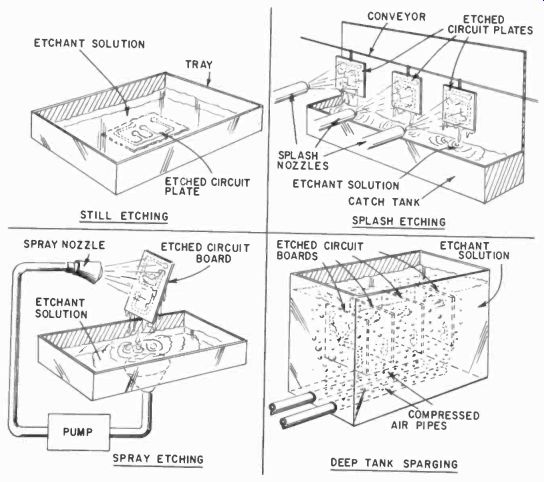
Fig. 213. A variety of etching techniques are used to prepare printed-circuit
boards.
Still etching
The material is immersed in a jar or tray. The etchant is then poured over the work and allowed to remain in contact with the work until etching is completed.
Splash etching
The work is mounted to a fixture which moves the work in place against violent streams of etching solution. The operation is limited to machine capacity in handling large numbers of plates.
Spray etching
The etchant is gently sprayed on the work.
Deep tank sparging
Large numbers of plates are immersed in deep tanks of etchant which is agitated by air streams blowing through nozzles.
These four techniques are shown in Fig. 213.
The most suitable approach for the amateur and experimenter is still etching. This method can be speeded by using brushes to simulate the splash technique, and experiments in sparging can be done with a small ear syringe or compressed air pump from a paint sprayer.
Take reasonable precautions with all etchants. Use rubber gloves and wear old clothing. A pair of safety glasses is a good investment if you plan any experiments in which the etchant is likely to splash. If you decide to use nitric acid, provide adequate ventilation for the gas fumes.
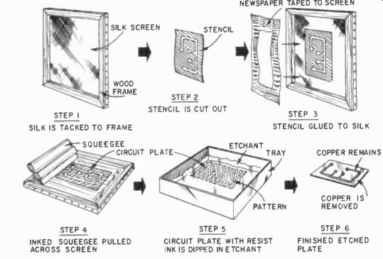
Fig. 214. The fundamental steps of silk screening.
Negative making
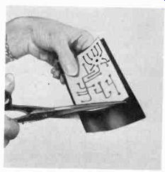
Fig. 215. The first step in the preparation of a silk-screen pattern is to
cut a piece of pre-sensitized gelatin film, slightly larger than the pattern
to be reproduced.
All resist-formation methods are variations of negative formation, whether they be stencils, silk screens, or tape and paint type of resists. The purpose of any negative is to prevent desired areas of the copper conductor pattern from being attacked by the copper etchant used to produce the final etched-circuit pattern.
Mechanical methods of etch resists
One of the popular mechanical etching methods uses silkscreen printing techniques. A resist material is applied through a silk screen stencil, and the resulting pattern is then etched. After etching, the resist is removed, leaving the finished etched-circuit pattern.
Silk-screen methods
There are many methods for laying out silk-screen patterns, but the basic one is to set up a stencil, part of which is opaque to paint and part of which will allow paint to come through. The paint is spread on the screen, on top of the work to be painted, and a squeegee is run over the paint, forcing it through those parts of the screen that have not been treated to prevent the passage of the paint. When the silk screen is removed from the work, the painted pattern appears. Basic silk screening is shown in Fig. 214.
Making your own silk screens
A pre-sensitized gelatin film is available for making silk screens." The material can be stripped from its vinyl plastic base, and toughened and transferred to a silk screen with very little difficulty.
Manufactured by the Craftint Co.
The first step in using this film is to cut a piece to a size slightly larger than the printed-circuit pattern "negative" ( Fig. 215 ).
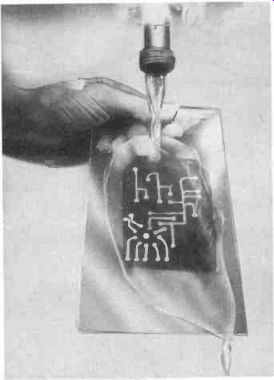
Fig. 216. Developing the exposed stencil material.
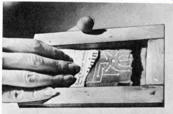
Fig. 217. Transferring the developed stencil to the silk.
The "negative" in this process is really a positive in the sense that, wherever a dark line on the negative appears, there will he a conductor in the final printed-circuit pattern. In this process, a "negative" can be made simply by using India ink on a sheet of celluloid or vellum. The "negative" and film sandwich are put into a printing frame and exposed to an arc light for 5 to 15 minutes, depending on the strength of the light and the distance from the light source to the printing frame. The rough side of the pre-sensitized film should be closest to the printed-circuit "negative." The exposure is made with the "negative" reversed in the frame.
The developer comes in powder or liquid form, and is used as a liquid at 65° to 75°F. The powder is mixed with water to make up a pint, quart or gallon, according to directions furnished on the manufacturer's package. Do the developing immediately after exposure to avoid fadeout and diffusion of the latent image into the gelatin by transferring the exposed film to the developer and rocking the film back and forth in the tray for 1 minute.
After development, place the film gelatin side up on an inclined glass surface and gently wash out the film with running water at 105° to 110°F. Use a thin stream, as shown in Fig. 216.
Wash until all details of pattern are clear and free from residues. Proper exposure will prevent loss of image due to over-washing.
Fig. 218. Finished stencil and silk mounted on I frame.
Prepare the silk by scrubbing it with hot water and mild detergent to remove any sizing or special treatment. Stretch the silk slightly and tack it to the frame.
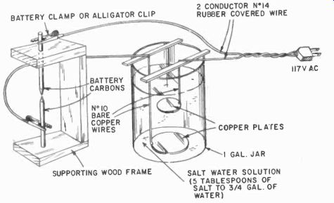
Fig. 219. Home-made arc lamp using old battery carbons and salt-water resistance
element.
Transfer the film to the silk by taking the film from the wash and placing it face up on a flat smooth surface. Bring the silk screen down on the film squarely and firmly, avoiding side-skidding motions. Then remove excess water with a blotter or newspaper, using flat, uniform pressure to give total adhesion of silk and gelatin (Fig. 217). A blue offset image of the "negative" on the blotter indicates good adhesion and proper exposure time.
Allow the film to dry naturally. When it is dry, the backing sheet normally peels by itself. Do not peel it unless the gelatin is completely dry. The screen and gelatin combination (Fig. 218) can now be used as a printing device for multiple runs of the printed-circuit pattern. A suitable resist is thinned asphaltum, which can be squeegeed through the screen on to the laminate boards.
Toughening and waterproofing the screen stencil
Where many runs are made, it is a good idea to toughen the stencil. The stencil is placed for about 5 minutes in a tray containing toughening-neutralizing solutions° and is then applied to the screen. Then it is baked for a minute or two at about 200°F with a heat lamp. About 4 to 6 inches between lamp and film is sufficient.
Exposure problems with pre-sensitized material
Some amount of trial and error is necessary in exposing this material. The manufacturer recommends using a test strip. Cut a film strip about 1 inch by 8 inches and place it in the printing frame with the rough side against the glass, facing the light source. Close the printing frame. Then put a piece of masking tape on the outside surface of the glass so that the tape covers all but 1 inch of the film.
Fig. 220. Using roll-tape resist to lay out a pattern.
Expose the uncovered section of film about 1 minute, and peel another inch of tape and expose 2 minutes. At the end of each succeeding minute, peel an additional inch so that, at the end of 6 minutes, the first 1-inch portion will have been exposed for 6 minutes, the next inch for 5 minutes, and so on down to the last inch, which was exposed only 1 minute.
Fig. 221. Fingernail polish can be used as a resist.
When developed and washed, the color of the 1-inch sections will vary from the original blue of the unexposed film to light blue on the 1-minute exposure. Proper exposure time will depend on the final film thickness required, and the lighting conditions.
Home-made carbon arcs are very effective, and one can be made from old battery carbons, as shown in Fig. 219. A salt-water resistance jar is used in series with the lamp and 117-volts ac.
Tape resists
Tape resists are mechanical resists made from various adhesive materials such as Scotch tape. They can be made or purchased in rolls and precut shapes such as circles and squares. The tape resists are put on the surface of the laminate (Fig. 220) and pressed firmly to secure positive adhesion. Tape resists must be joined tightly at conductor intersections and joints to prevent spoiling the circuit pattern by etchant leaking under the tape at exposed joints.
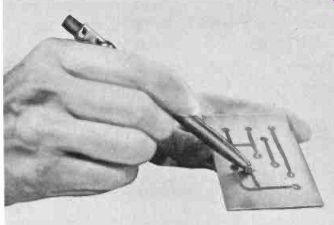
Fig. 222. Using a china marking crayon to lay out a printed-circuit pattern.
In an emergency, ordinary medical adhesive tape or cellulose Scotch tape can be used, although the heavier masking grades usually give better results.
Paint resists
Lacquers such as finger-nail polishes (Fig. 221) can be used to lay down a conductor pattern by brushing or by stencil methods. One of the more popular etched-circuit resists is asphaltum. Asphaltum is an asphalt-base paint obtainable at most paint stores and is easily thinned with petroleum solvents. Another source of asphalt is ordinary roofing tar or asphalt tile 4t, cement. Rubber cements are fair resists, and Duco cement can also be used.
Writing-implement resists
A common wax crayon can be used to outline the etched-circuit pattern on the laminate. This method has the advantage that, since crayons come in colors, more than one color can be used for initial layout purposes.
Two commercial "writing" type resists are also available. One of these is a ball-point pen containing a permanent ink which ...
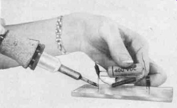
Fig. 223. A block
of plastic can he used as a bread board.
... normally resists alcohols, acids and alkalis at temperatures up to 850 F. A special version of this ink resists temperatures over 1,800°F. These pens come in various colors and can be used to lay out an etched-circuit pattern in color code. After etching the circuit, the paint is removed with organic solvents.
The other type of "written" resist is a liquid, also available in colors, dispensed from a ball-point tube. Each tube is good for over a mile of 1/16-inch-wide resist pattern. This ball-point tube material will resist nitric acid in etching processes.
Fig. 222 shows a China marking crayon being used to lay out a pattern resist. Many other items found around the house, such as wax-base eyebrow pencils and children's crayons can also be used.
Circuit layouts and design
The radio experimenter's breadboard technique can be used to advantage in setting up components for a printed-circuit layout.
After obtaining all the hardware and electronic components necessary for an experimental unit, the components are placed on a piece of medium-weight cardboard in the positions that will give the minimum layout area with a workable circuit. Be sure to figure in correct lead lengths and mounting-hardware clearances. After roughing in the circuit layout, be sure to locate the input and output terminations, and also any power-source terminations necessary. Lay out tube sockets and interstage components ( such as coupling transformers and R-C networks) in approximately the same order in which they appear schematically.
If possible, avoid two-sided conductor patterns because they are more complicated. Crossovers can be used if two-sided patterns are needed for size reduction. Crossovers and hole connections are discussed in a following section.
After all the components are in their final position, sketch in the common buses such as ground, B-plus and filament leads, and lay out all grid and plate leads so that they are isolated as much as possible from other leads. It is usually necessary to rearrange the components several times to determine the best combination for the layout. The components are then wired permanently and tested for final circuit operation.
One useful aid in breadboarding is a piece of Lucite or Plexiglas about 1/4-inch thick. Cut this to the approximate base size of the pattern desired. Heating component leads carefully with a soldering iron and pressing them into the plastic base will melt the plastic and allow the insertion of the component lead or mounting lug. When the soldering iron is removed the plastic cools and solidifies, leaving a rigid support for the component assembly. The technique is shown in Fig. 223.
Preparing the master drawing
If the conductor pattern is to be reproduced by photographic methods, a black-and-white master schematic is necessary for best results in final circuit production. For photographic reasons, the materials used in master drawings must have high contrast and be capable of giving sharp definition to the negative that is produced in the process. For average experimental purposes, use a good grade of Bristol board, but for finer work a plastic base material should be utilized. The two most popular materials are Stabilene ( a plastic-impregnated glass cloth) and Mylar. These materials are not subject to distortion due to changes in temperature and humidity. The manufacturer can furnish these with what is known as a "nonreproducible grid," that is, when the negative is printed, the grid lines will not show up on the sensitized laminate. The grid lines, however, are used as guides in laying out the conductor pattern.
Use a good grade of black ink, and scale the circuit to 2 to 4 times actual size. Small circuit layouts require more enlargement, and 8 or 10 times actual size is not uncommon where the detail must be brought out in the final negative. For reference purposes, a scale should be indicated on one corner of the original circuit, or one known dimension should be noted for a guide in photo copying the master.
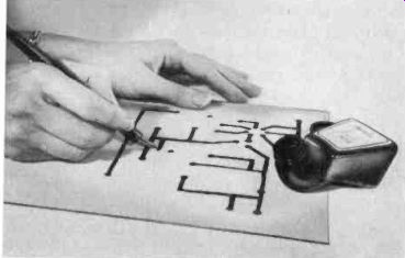
Fig. 224. Drawing a printed-circuit pattern with India ink. Conductor line
widths and spacings are described in Table 2-3 in regard to current ratings
in amperes. However, line widths between 1/16 and 3/16 inch are normal. Widths
narrower than 1/32 inch are difficult to maintain in the final etching process.
The large solid-copper areas should be broken up as much as possible to prevent
bridging and blistering of the foil on the laminate base if the pattern is
dip-soldered later. Circuitry should not be drawn any closer than 1/8 inch
to the edge of a part unless absolutely necessary. Conductor lines can be rounded
when making a 90° turn.
Heavy black circles at least 3/32 inch in diameter should be used where the circuit lines terminate. To obtain the best soldering results, the circles should be 1/16 inch larger than the hole which will be pierced in their centers during the final conductor fabrication. Draw letters so as to be at least 3/32 inch high in the final conductor pattern, and no less than 1/64 inch wide when reduced to size on the final negative.
The making of a master drawing is shown in Fig. 224. The master drawing is photographed by conventional processes to produce a sharp high-contrast negative, which is then used to print the final circuit-conductor pattern, using one of the sensitization methods described earlier.
Crossovers and holes
Occasionally it becomes necessary to cross over ( go from one side of the circuit board to the opposite side) with the conductor pattern. Several methods are used:
1. Eyelets,
2. Machine-screw connections,
3. Through solder on the circuit board proper,
4. "Plated-through" holes.
Table 2-3. Current Ratings of Copper Foil
Conductors rating for rating for conductor .001-inch .003-inch width thickness, thickness 1/32" 1/16" 1/8" 3/16" 1/4" 5 amperes 10 amperes 15 amperes 17 amperes 20 amperes 7 amperes 15 amperes 20 amperes 27 amperes 35 amperes
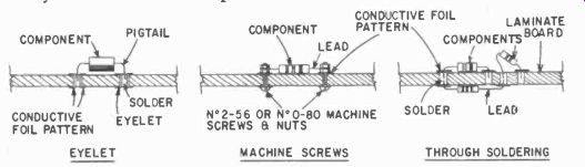
Fig. 225. Various techniques used for crossing leads from one side of the
board to the other.
The first three techniques, shown in Fig. 225, are suited to amateur and experimental use. Eyelets are usually used where components have to be changed frequently. After drilling the hole in the circuit board, the eyelet is placed in the hole and is "upset" or fastened into the board by flaring the smaller end of the eyelet with a center punch. The flared end can also be flattened into contact with the circuit conductor by "peening" or by pressure in an arbor press.
Some precautions must be mentioned in the use of eyelets for serious commercial work. Poorly plated eyelets will create noise and poor connections in critical circuits. Corroded eyelets will also produce unstable results in circuits subject to shock and vibration. Advanced workers prefer to use gold-plated eyelets for these critical applications.
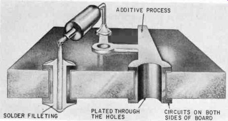
Fig. 226. The Thru-Con crossover system. (Courtesy General Electric Co.)
Plated-through holes
This is a commercial process in which the laminate is sensitized and, by a reverse printing process, the hole is prepared for plating directly through the thickness of the laminate board. After electroplating, the resist is removed and the excess foil is etched away, leaving a built-up electroplated through hole.
One patented version of this process is the Thru-Cons method. A sample of a Thru-Cone hole is shown in Fig. 226. The major advantage for this type of hole is that there is superior solder "filleting," which results in a more positive solder joint, the solder tending to lock up" on the component lead.
Machine-screw connections
This type of connection is for smaller quantities of boards where the circuitry is mainly de or low-frequency ac with no critical points. Small hardware such as 2-56, 1-72 and 0-80 screws, nuts and lockwashers are used to build this type of construction, which is very effective as an intermediate fabrication for pilot runs or prototypes. The possibility of high-resistance connections rules out permanent or large-scale use of this method.
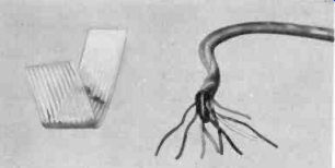
Fig. 227. Conventional multi-conductor cable and cable made with printed-circuit
techniques.
Through soldering of the circuit board proper
This technique should be employed only for small runs; the solder joints made in this way are not very uniform in size and quality. The solder should be permitted to flow down into the junction of lead and board conductor. The soldering iron should be removed promptly after soldering, to avoid blistering.
Laminates
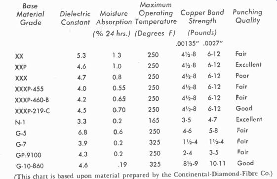
Table 2-4. Etched-circuit Laminate Properties
The majority of printed circuits are produced by variations of what are generally known as etched circuit techniques. A laminated base material consisting of a metal foil bonded to an
(This chart is based upon material prepared by the Continental-Diamond-Fiber Co.) insulating base is the starting point for etched methods. The techniques themselves will be described later. However, the experimenter should be familiar with the basic types of laminates and their main properties.
Making the laminate Laminates are made of a sheet of metallic foil bound in a hydraulic press to an insulating base. Sandwiches made of base material, adhesive, metal foil and stainless-steel press plates are put into a hydraulic press and cured under heat and pressure.
The base materials themselves are most often made of resin impregnated paper or cloth. The resins are usually thermosetting and cannot be melted again once the initial fusing and cure cycle has been performed.
Table 2-4 shows some typical laminates and their properties.
Flexible circuits
One unusual class of printed circuits is the flexible circuit.
Several commercial variations of these are made, including curved laminate boards formed to the mechanical requirements of the equipment. The flexible materials range in thickness from .001 inch copper foil on .010-.030-inch plastic films to .005-inch-thick copper on 1/16- and 3/32-inch thick resin-composition laminate base materials.
Flexible multiconductor flat cable
Fig. 227 shows an interesting bulk comparison between conventional multiconductor cable and flexible, flat, printed-circuit multiconductor cable. The latter, a recent development in printed circuitry, shows promise of great space and labor savings. Several manufactured types are available with variations in the number of conductors and their spacing, thickness and width.