SOONER or later, all electronic components fail to function properly; printed circuits and subminiature devices are no exception. The experimenter and technician should be familiar with the many techniques for restoring these units to working order. Many printed-circuit units ( such as ceramic-based types where components are "fired" on) are usually cheaper and easier to replace than to repair.
The most important difference between ordinary wired circuits and printed circuits is the uniformity of the latter. Thus, once a service technician learns how to trace a particular printed circuit, he will not have to learn a new arrangement of components and wires the next time he troubleshoots the same circuit Many manufacturers of printed circuits also identify components by stamping or coding on the printed-circuit board, which aids the technician considerably. One other helpful feature of printed-circuit boards is that they often resemble the schematic as far as physical layout is concerned. Some manufacturers also bring out a set of test points, which helps immeasurably in rapid testing.
Armed with a knowledge of the possible troubles to be encountered, the precautions to be observed and the testing techniques and tools used, the technician can master any printed-circuit repair.
Possible troubles and diagnosis
The major servicing troubles in printed circuits usually fall into five categories, some of which are interdependent, according to the circuitry. The five repair classes are ( 1 ) circuit opens, ( 2 ) circuit shorts, (3) circuit intermittents, ( 4 ) defective soldering and ( 5 ) mechanical defects.
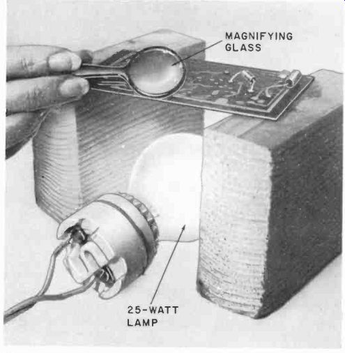
Fig. 501. Magnifying lens and 25-watt lamp used to detect printed-circuit-opens"
Open circuits crop up frequently and most are probably due to the size of the conductor used in some parts of the circuit.
Many conductors carrying a low-voltage low-current signal, such as a 1.4-volt 50-ma filament circuit bus bar, could be less than 1/32 inch wide as shown in Table 2-3, Section 2. Although minimum practical widths are closer to 1/32 inch, this figure is still small compared to solid No. 18 or No. 20 hookup wire.
Bending of the board in shipment, vibration during use or slight inclusions in the foil during manufacture can all lead to opens.
Another pause of open circuits is failure of components themselves. A transformer winding can open due to an overload, or a resistor can open due to repeated overloads or excessive heat.
Sometimes the process is reversed and, instead of the copper-foil conductor opening due to component failure, the foil opens and a string of components go.
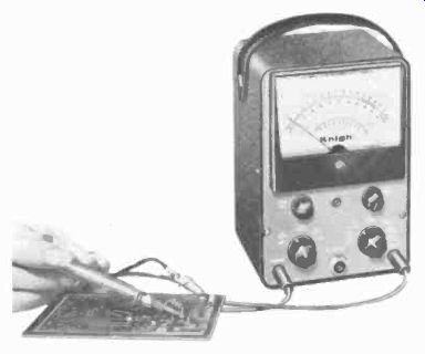
Fig. 502. Using a vtvm for point-to-point circuit checks. (Courtesy Allied
Radio)
Opens are detected with point-to-point measurements or by visual inspection. Two handy items for visual inspection are shown in Fig. 501-a 25-watt lamp on an extension cord and a magnifying glass that can often locate opens by visual observation. The 25-watt lamp will not throw too much heat and can be used for long periods of time without eye fatigue. Where board thickness and component density are high, a 60-watt lamp should be used. However, the 60-watt unit throws off considerable heat and cannot be held too close to the circuit board or key components for long periods of time. Point-to-point measurement with a vtvm is shown in Fig. 502. A signal generator can be used for opens detection, remembering, to keep the output as low as possible since high-level signals are usually fatal to components such as transistors or ultra-low-level milliwatt-range, transformers.
Circuit shorts are often caused by dirt, faulty components or loose wire ends and solder particles. When repairing printed-circuit and subminiature assemblies, shake off excess solder and component lead cutoffs, as described under detailed servicing instructions. For the same reasons, steel wool or emery paper is not recommended 'as a cleaner for printed-circuit assemblies since these materials can, leave conductive particles in small crevasses and cause shorts.
A short can also often be detected visually by a "sunburst" pattern of copper caused by sudden overloading and vaporization of the foil.
A very annoying type of short is caused by gradual dirt and moisture building up between two conductors that are normally insulated from each other. This partial, or high-resistance, short often resembles a resistor in its effects and is sometimes hard to find visually. The dirt in high-resistance shorts can be removed with a toothbrush and solvent. The cleaned base board is then coated with resin to prevent the re-entry of dirt and moisture.
Defects in the printed-circuit base-board material itself and "silver migration" often lead to partial short circuits. The only remedy is to drill out the offending portion of the board.
Intermittents, whether printed-circuit or not, have always been a bane to service people. Intermittents in printed circuits usually pop up in locations where there is mechanical stress such as near tube-socket tabs, component lead-ins ( eyelets, crossover and through-board connection points) or sometimes in the leads themselves. A bent pigtail that has been re-formed a few times in repair or in manufacture tends to be brittle, and might even crack when the board is in certain positions. The application of heat, humidity or vibration will help "smoke out" an intermittent.
Gently tap the printed-circuit board while the area is checked visually or with instruments. If vibration fails to show up the intermittent, a 60-watt lamp can be held near the suspect area for short periods of time and the board allowed to cool between checks. Sometimes the expansion due to heat will open up the intermittent and thus pinpoint the trouble.
Mechanical defects come from such things as improperly eye-letted holes, poor riveting in original manufacture, and component mounting hardware which puts strains on printed-circuit boards. Check every point at which a component is mounted to the board by mechanical means such as springs, clips, nuts, screws, clamps and brackets. This class of defect is very often obvious from mechanical inspection under the magnifying glass. The remedy is usually a mechanical adjustment with a screwdriver or pliers, and occasionally a small soldering job in the case of some broken parts. Broken dials. springs and items affected by heat must he replaced.
Pitfalls in printed-circuit servicing
Because of the overall compactness and close component locations in printed circuits, certain pitfalls await the technician who attempts a hasty job.
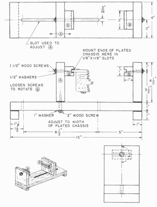
Fig. 503. Some pieces of scrap wood can be used to make a very convenient
holding jig for printed circuits.
The first hazard is the possibility of damaging the etched circuit foil. Some components are attached to the base in such a way that their removal may cause tearing or peeling of the copper foil.
Replacement of the foil is described later in this section.
Damage to the base board proper is another source of headaches. Most printed-circuit boards are thin and cannot be bent too much without cracking. Printed-circuit boards should not be gripped on their corners with pliers or put in vises in a way that the weight of the board will make it sag and crack. Simple holding jigs can be made up from scrap wood ( Fig. 503). If a vise must be used, pad the jaws with felt or sponge rubber and tighten the vise just enough to hold the board securely without bending it.
Excess heat can be ruinous to a printed-circuit board by either blistering the copper foil or actually degrading the base material.
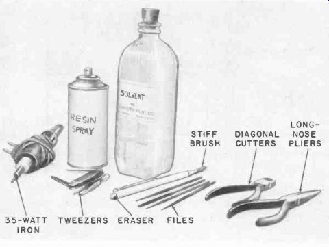
Fig. 504. Some typical tools used in printed circuit repair.
Soldering irons over 60 watts in size should be kept far away from ,printed-circuit boards. Likewise, blowtorches and soldering guns should never be used for printed-circuit and subminiature repairs.
Heat is the result of both temperature and time, and a 25-watt or 35-watt soldering iron can cause as much damage as a 60-watt iron if left on a joint too long. Be careful around soldered joints that cannot conduct heat away fast enough. The old trick of using pliers or an alligator clip for a heat conductor can come, in handy here.
Another common printed-circuit repair hazard is the over abundant use of solder. It is extremely easy to get too much solder on a printed-circuit joint, especially if the technician is new to the work and has been soldering conventional wiring for many years. A brush and pick can be very helpful in cutting down excess solder problems.
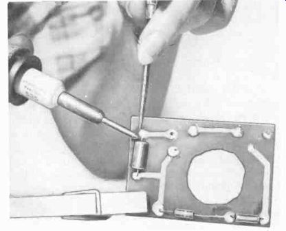
Fig. 505. The ordinary clothespin can make a convenient third hand when working
with printed circuits.
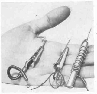
Fig. 506. An assortment of ' home-made test prods.
Tools
Shown in Fig. 504 are the tools recommended for printed-circuit repairs. A 60-watt iron is used on those extra heavy jobs such as brackets, supports and corners where large amounts of heat must be applied for very short intervals. Ground lugs can be soldered faster with a 60-watt iron. However, the 60-watter should be reserved only for those jobs where the 25- and 35-watt units have failed to give results. The 35-watt iron is the workhorse of printed circuit repair, and hints on its use are given elsewhere in this section.
When repairing printed circuits, it is always wise to coat the repaired portions of foil with an insulating medium. Several chemicals have been developed for this purpose, most of them resin-base lacquers. They can be applied either by brush or spray can. In an emergency, fingernail polish and polystyrene Q dope can be used. A solvent and soft cloth are handy to have around also.
Common solvents are carbon tetrachloride, chloroethylene and wood alcohol. Carbon tet should be avoided unless the work area is well-ventilated.
An assortment of picks is a necessary item in printed-circuit repairs. In addition to removing solder deposits, the pick is often the only way to move or bend a hidden lead to where it is accessible for work. A Fiberglas brush or toothbrush is a must for flicking off excess solder and general cleaning of printed-circuit boards. The Fiberglas, being abrasive, can be used to shine up Copper foil prior to soldering; a Fiberglas eraser is particularly convenient for this type of work. An ink eraser with an abrasive rubber core is a good substitute.
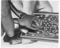
Fig. 507. Replacing a capacitor on a printed-circuit board.
A small pocket knife with a few blades is handy for scraping joints or component terminals prior to soldering. A set of tweezers is also useful for handling parts too delicate for a needle-nose pliers.
Side cutters and needle-nose pliers are indispensable for printed-circuit repairs. Several jeweler's models, smaller in size than regular pliers, are ideal. A good set of assorted-shape Swiss needle files can be worth their weight in gold when fitting in new components or adapting standard hardware to unusual mechanical situations.
Clothespins ( Fig. 505) can be used effectively as third hands.
Felt inserts should be used to protect the printed-circuit board surfaces.
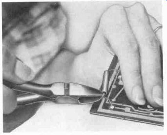
Fig. 508. If the leads are long enough, they ran be cut close to the body
of the resistor. Additional lead length can be obtained by cutting the resistor
in half and crushing the resistor body.
Home-made test prods ( Fig. 506) can be assembled from miniature alligator clips and sewing needles. The variety of prods is limited only by the user's ingenuity. A piece of plastic tubing or spaghetti is slipped over the prod to eliminate short circuits when using the prod in close quarters.
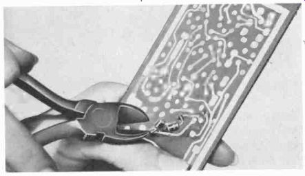
Fig. 509. After being cut apart, the two halves of the resistor are separated.
Replacing components
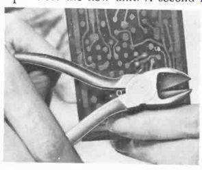
Fig. 510. Crushing the body of the components in the crotch of the pliers.
Components can be replaced in several ways. One method is to cut the old component in half, strip the component body off the lead wires, and use the extra lead from the inside of the component as a tie point for the new unit. A second method, where leads of the defective component permit, is to cut close to the component ends and use the old leads as new starting points.
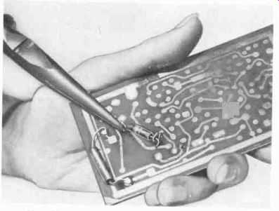
Fig. 511. Soldering the new component into place.
Still another technique is to remove the old component completely and repair or replace as tests indicate. Before removing a component, be sure to check it even if the circuit makes it appear that it is defective. Be sure that no other component or wiring is in parallel with the suspected component, by opening one lead of the component.
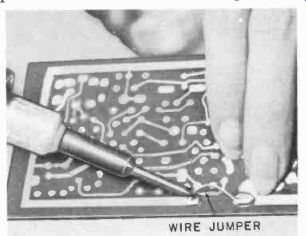
Fig. 512. Using a wire jumper to repair a broken printed-circuit conductor.
Fig. 507 shows a capacitor which has short leads. A diagonal cutter is used to clip the component in half, and then the remaining parts of the component are removed by pinching carefully with the pliers. Sometimes space permits mashing the component body remains in the crotch of the pliers. Be careful to hold the printed-circuit board in such a way as to allow the "mashings" to drop away from the remaining circuitry. The exposed wires are scraped clean with a knife. Avoid nicking wires by scraping at an angle to the wire. The leads of the new component are looped around the old leads with a needle-nose pliers, and the new component is then soldered in place.
Fig. 508 and 509 show the removal of a resistor which has long pigtail leads. The remains are mashed in the crotch of the pliers (Fig. 510). The leads can then be re-formed into loops, and the new component dropped in and soldered ( Fig. 511). Excess lead wire should be clipped short, making sure the clippings fall away from the hoard where they might cause short circuits.
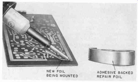
Fig. 313. Using adhesive-barked foil to repair a broken conductor.
Complete replacement of component
One system for removing components has been named the "10-step method."
1. Determine which component is at fault.
2. Remove defective component by cutting it away from board.
3. Remove any resin coating from the connection to be reworked, using solvent or abrasive brush.
4. Remove solder from connections to be replaced, making sure solder flows away from board and adjacent circuitry. Use a brush and pick if necessary.
5. Take off remaining leads with pliers ( in case of delicate components, use tweezers) while an iron is still held on the work momentarily to melt solder.
6. Open webbed mounting holes by inserting a pick or knife in the 'hole while the solder is still soft. After the solder cools, clean the area around the repair with solvent or an abrasive brush.
7. Fit the replacement component into existing mounting holes, taking care not to damage the original foil.
8. With an abrasive brush clean connections on the component being soldered in and solder in. A soldering preform such as a washer or ring of solder wire can save time when soldering in spots that are crowded.
9. Check the soldered joint with pick or knife. Pry the joint gently and look for evidence of cold solder and joints held by flux only.
Rework if necessary.
10 Clean off excess flux and any solder particles. Recoat reworked areas with a protective resin.
Replacing foil
Two methods are in use for replacing foil that might be broken in the repair process. One of these is to use a small piece of hookup wire as shown in Fig. 512.
The second method ( Fig. 513) employs a repair foil which is adhesive backed. First, outline the path of the old foil on the printed-circuit board with a pencil or scriber made from a fine needle point. Next, put a piece of tracing paper over the defective section just marked out, and trace the outline of the section on the paper. Allow extra foil for overlapping the new foil on the old copper foil. Remove the tracing paper and paste it on the adhesive-backed copper-foil repair material. Using the outline on the tracing paper, cut the foil to pattern and remove the tracing paper.
Clean with solvent the area to be reworked and use an abrasive brush to clean and roughen the surface of the printed-circuit base board. Then put the adhesive side of the cut-out foil nearest the copper foil already on the board, and press down. Use a chisel-tip soldering iron to heat the foil and cure the adhesive. It takes about 1 to 1 1/2 minutes to get a fully cured adhesive bond between the new foil and the base board. Finally, solder the new foil to the old foil along the edge at each end.
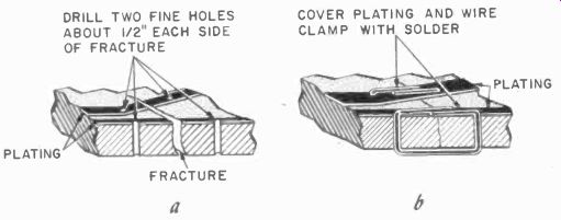
Fig. 514. Steps in the repair of a fractured board. Two fine holes are drilled
and wire clamps are inserted. The clamps are then soldered. (Courtesy Motorola,
Inc.)
Repairing cracked boards
Simple cracks in areas not subject to stress by heavy components or mounting hardware are easily repaired ( providing no conductors cross the cracks at any point) by using fast drying plastic cement. Although cracks like these are seemingly harmless they must be repaired to prevent their spreading into areas where they can affect circuit function and to maintain the overall strength in the board.
When a crack occurs in a circuit area, crossing conductors must always be repaired. Sometimes the conductor may not seem to have been harmed, especially, if the crack is. a hairline. Nevertheless it must be repaired, for it has been weakened.
Drill fine holes in the board as shown in Fig. 514 and insert wire clamps. By proper positioning, the clamps are used to support conductors crossing the line of the break. When the supports have been inserted and the edges of the crack drawn together, coat the clamps and the associated conductors with solder.
Tube-socket repairs
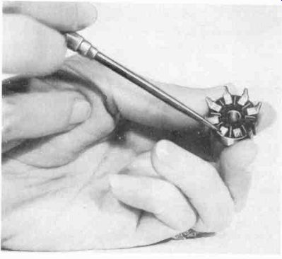
Fig. 515. Use a pick to clean the contacts of a tube socket.
Printed-circuit and subminiature tube and transistor sockets are a frequent source of trouble. The causes are usually dirt, flux, oxidation and mechanical difficulties such as loss of spring tension or distortion in the contact spacing.
In the case of poor spring tension, a pointed pick or probe can be used to bend the contacts of the weakened spring back into a useful position. This requires patience and slow, gentle manipulation of the bending tool. Distortion of the contact spacing, such as incorrectly positioned contacts, can be detected by comparing the socket to a tube base-pin pattern overlay. Sometimes incorrectly positioned contacts can be aligned by resoldering the tabbed end. In other cases, where the molding process is such that no amount of tab bending or resoldering will realign the contact, complete replacement is the best answer.
Dirt and light surface corrosion and oxidation can be removed by scratching the contact with a pick or needle inserted in a piece of 1/4-inch dowel. Very sparing application of chemicals such as General Cement's De-Oxid sometimes helps dissolve oxidized residues. If flux remains from a previous assembly, dissolve this by using a flux solvent from an eye dropper. Abrasives, such as steel wool, should not be used for cleaning tube-socket contacts because of the danger of short circuits or partial high-resistance shorts due to particle accumulations. The socket scraping operation is shown in Fig. 515.
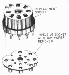
Fig. 516. Inserting a new socket in a printed-circuit board with out removing
the old. (Courtesy Sylvania Electric Products. Inc.)
Replacement of sockets
Wherever possible, the socket should be removed by unsoldering one contact at a time, brushing the excess solder away, and prying up the socket tab with a knife or other thin-bladed tool. The socket can also be removed by cutting the tabs with a diagonal pliers, but this is not always possible due to cramped space or other components near the socket which might be damaged by the pliers. The ground terminal is usually unsoldered last, and the socket then gently pried loose and free from the base board. The grounding section of the copper foil sometimes breaks and should be replaced with new foil or wire.
Depending on the mechanical mounting details, it may be necessary to enlarge the old mounting hole when installing a new socket. The new socket should be as close to an exact replacement as possible. The socket hole ( and, where required, the tap holes ) can be enlarged conveniently with a small needle file. If the new socket is slightly oversize, it can be filed down to fit the hole in the base board. If the new socket is undersize, a coat or two of cement will aid in building up the outside diameter of the socket base to a snug fit.
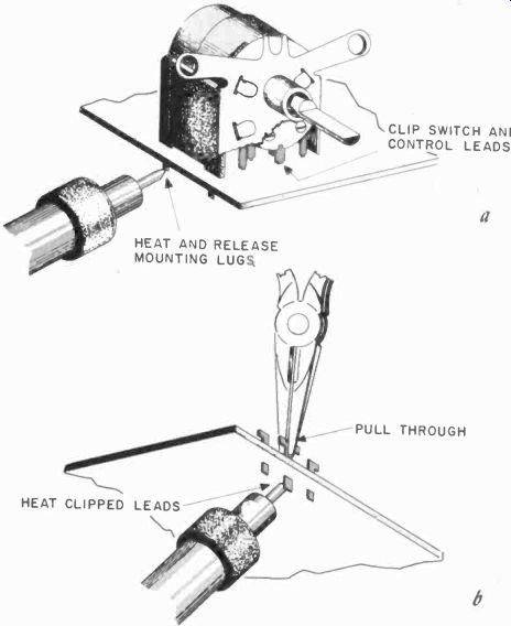
Fig. 517. Method for removal of controls and switches from printed-circuit
boards. (Courtesy Sylvania Electric Products Inc.)
By using specially prepared sockets it is possible to replace a defective wafer type socket without having to subject the foil to both unsoldering and soldering. Remove the top half of the wafer socket with diagonal cutters. Work carefully, a small section at a time, to avoid damaging the printed-circuit hoard. Remove all broken socket clips from the old socket and then insert a new one ( Sylvania type) as shown in Fig. 516. Next, solder the lugs and the job is done, Replacing transformers, inductors and if's Miniature if's and rectangular potted inductors generally have four to six soldering lugs, and are originally mounted by inserting these lugs through punched holes in the printed-circuit board.
The lugs should be unsoldered and bent up one at a time, brushing off excess solder. After the lugs are bent up, it is possible to remove the component by bending the lugs perpendicular to their respective slots in the printed-circuit board and sliding the component off the board. The new component should be an exact replacement to minimize mechanical rework on the .base board.
Tabs on the new component can either be bent in place or soldered into the new position. Because of the size and materials used in making the cans or if's and other inductors, component layout must be studied carefully before attempting an exchange.
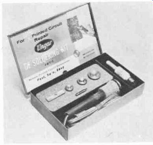
Fig. 518. Desoldering kit designed for use with printed circuits. (Courtesy
Ungar Electric Co.)
It is also helpful to mark the position of any keyed part ( such as a slot or special ear on the old component) on the board so that there will be no error in relocating the new unit.
Replacing controls
Controls and switches can generally be treated the same way as other multiple lug components. To replace units mounted directly on the printed circuit board, cut the leads to the assembly about 3/4 inch above the chassis ( Fig. 517-a ). The mounting lugs are unsoldered and bent perpendicular to the chassis one at a time. The entire component is then gently removed from the board. The component lead' stubs are left attached to the board at this point. They are removed easily, one, at a time, by unsoldering, straightening if bent, and pulling through the chassis (Fig. 517-b ). The mounting lug slots and component lug holes are then cleaned with a pick, brush and iron. The new control or switch is mounted and all connections are soldered, completing the job.
Special de-soldering methods
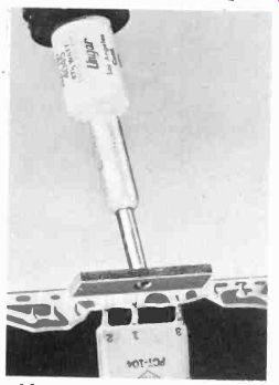
Fig. 519. This soldering-iron lip, in the shape of a bar, can he used to remove
packaged components. (Courtesy Ungar Electric Co.)
Shown in Fig. 518 is a special kit containing cup, bar and slotted soldering-iron tips for printed-circuit repair work. The tips are made of chromium-copper alloy. In addition, they have been designed to radiate very little heat along their sides and edges.
This promotes heating of the parts to be removed without disturbing nearby components. The tips are interchangeable within the heating element.
The bar type tip ( Fig. 519) is designed to remove straight-line components such as packaged circuits and resistor-capacitor combinations. The bar is held against the terminals until the solder melts, and then the component is lifted or allowed to fall off.
Cup-shaped tips ( Fig. 520) have been designed in 5/8-, 3/4- and 1-inch diameters to fit the common miniature tubes as well as larger-diameter components. They are suited for removing sockets as shown in Fig. 521. The cup is positioned over the component tabs or lugs and the component is removed by gentle prying when the solder melts.
The slotted tip is perhaps the handiest of the series, acting both as soldering-iron tip and miniature crow-bar. It is used to straighten bent tube tabs or other component leads. The slotted tip is held against the solder until the latter melts, and then the slot of the tip is positioned around the tab or lead to be removed.
Gentle prying completes removal. Fig. 522 shows the slotted tip being used to bend up a component lead prior to removal.
In many cases, it will not be necessary to remove a printed-circuit board from a chassis for servicing. The versatility of the tips allows the user to apply plenty of heat in tight spots.
Another special soldering technique especially useful when removing multiple-lead components is illustrated in Fig. 523. The soldering pot, a thermostatically controlled unit, is an invaluable bench aid. You just dip the board into the molten solder and remove the component. When replacing single-lug components return to the soldering iron.
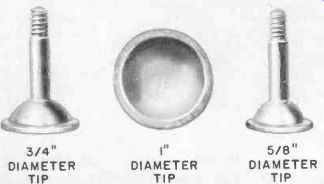
Fig. 520. Cup-shaped solder tips for removing tube sockets from printed-circuit
boards.
Test instruments
Although specialized test instruments are not necessary for servicing printed-circuitry, the service technician would do well to add a few items to his bench line-up. In order to do this economically and at the same time gain useful working knowledge of printed-circuit techniques a few useful circuits which are easily constructed are included in this section.+
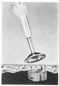
Fig. 521. Removing a tube socket with a cup-shaped soldering-iron tip. (Courtesy
Ungar Electric Co.)
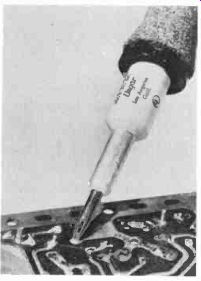
Fig. 522. Slotted soldering-iron tip being used to bend up the lugs of a multiple-lug
component. (Courtesy Ungar Electric Co.)
In-circuit component tester
After isolating a malfunctioning stage many technicians rely upon clip-and-check methods to test suspect components. One lead of the component is removed from the circuit to isolate it so that it can be tested for changed value, shorts, and in the case of capacitors, leakage. This procedure is one that is efficient up to a certain point. When working with printed-circuitry, where manipulation must be kept to a minimum, the clip-and-check method becomes a search for more than a malfunctioning component-it's looking for even more trouble. The chance of damaging a good component when resoldering and the possibility of cracking the board more than offset the convenience of troubleshooting in this manner. In-circuit checkers are a must when servicing printed circuitry. The instrument shown ( Fig. 524) is a combined R-C bridge and quick-check unit, which is particularly suited for servicing.
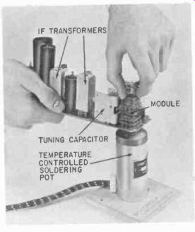
Fig. 523. A number of connections can be soldered (or unsoldered) in one operation,
when using a soldering pot. (Courtesy Motorola. Inc.)
The only disadvantage in using instruments of this type arises when the circuits being probed use transistors. The 20 mhz and 60-cycle waves put out by these instruments for test purposes can damage transistors. Remove all transistors before using any instruments of this type.
Fig. 524. Combined R-C bridge and in-circuit checker for servicing printed
circuits. (Courtesy Allied Radio.)
Subminiature tube tester
The printed-circuit board for a subminiature tube tester is shown in Fig. 525. The flea clips for the tube leads and the switches are also shown in the photograph. Construction details for the unit are given in Fig. 526. Designed for both 0.625- and 1.25-volt filaments, the tester contains a resistor R2 for extra protection when checking lower-voltage tubes.
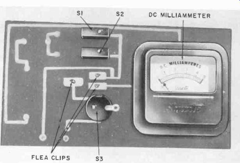
Fig. 525. Photo of the subminiature tube tester taken while the unit was under
construction.
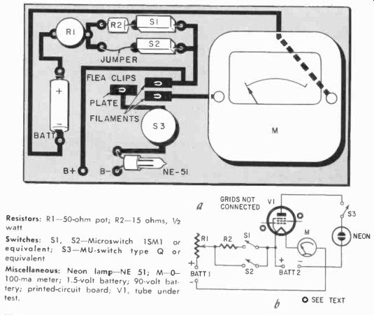
Fig. 526. Layout of the printed-circuit board and circuit diagram for a subminiature
tube tester.
Resistors: R1-50-ohm pot; R2-15 ohms, 1/2 watt Switches: S1, S2-Microswitch 1SM1 or equivalent; S3-MU-switch type Q or equivalent Miscall :
Neon lamp-NE 51; M-0 100-ma meter; 1.5-volt battery; 90-volt battery; printed-circuit board, V1, tube under test.
Fig. 527. The layout of the printed-circuit board of the transistor checker is shown at the left. The circuit diagram appears above.
----------
Resistors: R1-2,000 ohms, 1/2 watt R2-1 megohm pot (Lafayette Radio VC-47 or equivalent) R3-51,000 ohms, 1/2 watt.
Switches: 51, S2-miniature spst rotary; S3, S4-dpdt slide type Motor: 0-5-ma dc (Shurite 4302 or equivalent)
Only the two filament leads and the plate lead are used in this checker, which tests for filament continuity and leakage. It's a good idea to use a vtvm or high-resistance vom as a check when setting R1 to obtain the right voltage across the filament of the tube under test. The neon lamp will flash when S3 is depressed if there is leakage from the plate to other tube elements.
Simple transistor checker
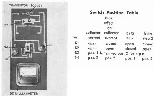
Fig. 528. Photo of the transistor checker. The arrangement shown here follows
the circuit diagram fairly closely.---
Switch Position Table
A simple transistor checker is shown in Figs. 527 and 528. The emitter is used as the common ground with resistor R2 varying the base voltage. This test circuit is meant to be used as a static checker-no signals pass through the transistor.
Three tests can be made-shorts, opens, and gain. To test for shorts switches S1 and S2 are opened, S4 is flipped to position 2 and current in the collector circuit read on the 5-ma meter.
The reading will depend somewhat on the collector resistance setting but will usually be in the order of 10's or 100's of micro amps. A reading in milliamps indicates a short or leakage. For precise results, the manufacturer's data should be checked to determine the collector current for specific collector bias voltages with the base open. An open check is made by closing the base circuit switch S1, opening S2 and then increasing the series resistance in the base circuit. With less base bias voltage, the collector current should rise. If no change occurs, there is usually an open in the transistor.
Gain is checked by flipping S4 to position 1, opening S1 and closing S2. Then set the base resistance to produce a fixed current, say 50 microamps, on the meter. Move S4 to position 2, close S1, open S2, and read the collector current while the base is still biased for the 50 microamps. Collector current divided by base current is used as a rough check of gain, sometimes called the beta of the transistor. Checks for n-p-n units can be made by using S3, which reverses the battery.
A summary of switch positions is given in Fig. 528.