AMAZON multi-meters discounts AMAZON oscilloscope discounts
THE transistor basically is a current-operated device. Current amplification therefore is inherent in it. The base-to-collector amplification factor (beta) expresses the extent to which common-emitter or common-collector transistor circuits will amplify currents.
Direct current and voltage amplifiers using transistors are simple and straightforward, often more so than ac amplifiers. In most such basic circuits, high, true current gain is possible.
This section describes several practical dc amplifier circuits. The resistance-coupled circuits will be seen to bear a close resemblance to direct-coupled vacuum-tube amplifiers. The direct-coupled transistor amplifier, on the contrary, has no counterpart in tube practice.
Single-stage current amplifier
Fig. 301 shows the circuit of a single-stage direct current amplifier in which amplification is provided directly by the common-emitter beta of the transistor. Because beta is a short-circuit parameter, the load device connected to the DC OUTPUT terminals must have low resistance. High values of load resistance decrease the current gain.
The load resistance should be 100 ohms or less.
With a dc supply (B) of 1.5 volts a current gain of 40 is obtained:
25 microamperes input will give an output-current increase of 1 ma.
(This is very nearly the full beta value of 45 for the Raytheon CK721 transistor.) The steady direct current (ic) flowing when the DC INPUT terminals are open is 100 µa.
The current gain and the zero-signal collector current vary with the resistance of the source to which the DC INPUT terminals are connected. The zero-signal collector current and the current gain both decrease as the input resistance decreases.
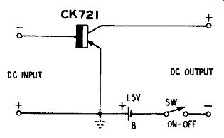
Fig. 301. Single-stage current amplifier.
Since ico and beta both vary with temperature, this rudimentary amplifier is suitable only in applications in which the ambient temperature can be stabilized. In spite of this shortcoming, however, its simplicity and high gain fit this amplifier for use between a high-resistance dc source and a low-resistance load device (such as relay or model actuator).
Transistors with higher beta ratings will provide higher current amplification. Raytheon CK725 and 2N65, for example, have maximum current gains of 90.
Single-stage current amplifier with fixed-resistance input The tendency of current gain to vary with input (generator) resistance in the simple direct-current amplifier may be minimized to a large extent by fixing the input resistance by means of a relatively low value of shunting resistance, R (Fig. 302).
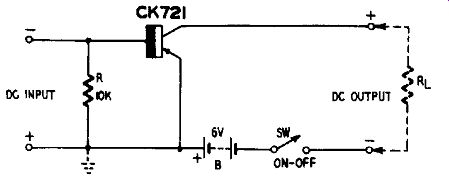
Fig. 302. Single-stage current amplifier with fixed input resistance.
While the presence of this resistor reduces the current gain to 25 (i. e., 40-ua input gives a 1-ma output-current increase in an external load R1, not exceeding 100 ohms) this gain is stabilized against the large changes usually encountered when the generator resistance varies from a few ohms to several megohms.
At the measured current gain of 25, the input resistance of the stage is approximately 10,000 ohms, dc input voltage 0.5 volt, dc input current 40 va, zero-signal collector current 100 ua and maxi- mum-signal collector current increase is 1.0 ma (that is, from 100 to to 1.1 ma) .
Increasing the external load resistance RL, decreases the gain.
For example, raising RL to 1,000 ohms drops the gain 10.
Cascaded p-n-p current amplifier
Fig. 303 shows how current-amplifier stages may be direct-coupled for increased gain.
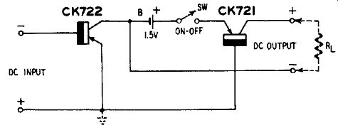
Fig. 303. Cascaded p-n-p current amplifier.
In this circuit, the collector output current of the first transistor (Raytheon CK722) flows directly through the base-emitter circuit of the second transistor (Raytheon CK721) . The input current thus is amplified successively by the CK722 and CK721.
Both stages are connected as common-emitter dc amplifiers and the 1.5-volt battery (B) supplies both collectors. A dc input of 10 ma gives an output-current increase of 1.0 ma through a load resistance RL of 100 ohms or less. This represents a current gain of 100 times, or 40 db.
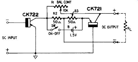
Fig. 304. Cascaded current amplifier with balance control.
The zero-signal collector current of the CK721 output transistor is the sum of the CK721 zero-signal current (ico) and the amplified zero-signal current of the CK722. This initial current is large enough to be troublesome in some applications. However, it may be bucked out by means of any of the conventional balancing circuits.
Fig. 304 shows how a balancing circuit be added for setting the initial collector current to zero. Here the bucking circuit is a four-arm bridge consisting of resistors R1, R2, R3 and the internal collector resistance of the CK721. Arm R1 of the bridge is made vari able for adjustment. When the bridge is set to null by adjustment of R1, the current through the load resistor RL is reduced to zero and only the current change due to application of the input signal will flow through it.
All common-emitter, direct-coupled, current amplifier circuits employing a single battery have the slight disadvantage that there is no ground terminal common to both input and output. Thus, the input or output may be grounded but not both simultaneously.
To employ a common ground, a separate battery must be used in each stage. Otherwise resistance coupling must be employed.
Cascaded p-n-p / n-p-n current amplifier
The effect of the amplified zero-signal collector current of the input transistor in a two-stage direct-coupled current amplifier is minimized by employing a p-n-p (Sylvania 2N34 in Fig. 305) in the input stage and an n-p-n transistor (Sylvania 2N35) in the output stage. The zero-signal collector currents in the two transistors are in opposite directions. This circuit sometimes is called a complementary-symmetry dc amplifier.
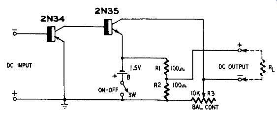
Fig. 305. Cascaded p-n-p / n-p-n current amplifier.
Here, as in the previous two circuits, a single 1.5-volt battery (B) supplies the two transistors. Since the n-p-n and p-n-p collectors require voltages of opposite polarity, the battery is connected in series with the output-stage emitter. Negative voltage thus is applied to the 2N35 emitter and (through the emitter-base circuit of the 2N35) to the 2N34 collector.
The balancing circuit is similar to the one explained previously in connection with Figs. 303 and 304. It consists of a four –arm bridge (R1, R2, R3 and the internal collector resistance of the 2N35) . When R3 is set for null, no dc flows through the external load resistance.
With 0.4 µa dc input, this amplifier delivers an output of 100 µa through a 1,000-ohm load resistance RL. This represents a current gain of 250 times, or 48 db. With the amplifier delivering full output, drain from the 1.5-volt battery is 7.5 ma dc.
Single-stage dc voltage amplifier Fig. 306 shows the circuit of a single-stage, resistance-coupled, dc voltage amplifier employing a Raytheon CK721 transistor. With a ...
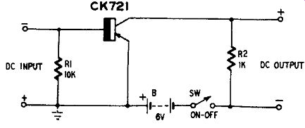
Fig. 306. Single-stage de voltage amplifier.
... measured input resistance of approximately 2,550 ohms, this amplifier provides a voltage gain of 5. For an input signal of 0.2 volt, the output-voltage change across collector resistor R2 is 1 volt. The zero-signal voltage drop across R2 is 2.4 volts, which may be nulled by applying a bucking voltage in series with the top of R2 and the positive DC OUTPUT terminal. Current input is 80 µa and the corresponding output-current change is 1 ma in R2.
Cascaded dc voltage amplifier Resistance-coupled dc voltage amplifier stages of the type de scribed in the preceding section may be cascaded, as shown in Fig. 307, for higher voltage gain. Transistor noise is the factor limiting the number of stages which may be coupled in this manner.
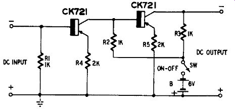
Fig. 307. Cascaded dc voltage amplifier.
Employing two Raytheon CK721 transistors, this resistance-coupled circuit provides a dc voltage gain of 25. With an output of 1 volt, the dc input signal is 40 my.
Single-stage power-type current amplifier
The circuits described up to this point, while providing high gain, handle relatively low current levels. By substituting a power transistor for the conventional type, larger currents may be accommodated. Fig. 308 shows such a circuit.
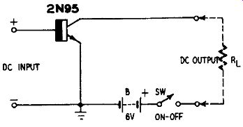
Fig. 308. Single-stage power-type current amplifier.
Here a Sylvania 2N95 power transistor is operated at 6 volts.
Providing a current gain of 35, this single stage provides a dc output-signal increase of 250 ma in response to a dc input signal of 10 ma.
The initial, zero-signal dc collector current is less than 10 ma. To utilize most fully the rated beta of the 2N95, the external load resistance RL must be 1 ohm or less. This low resistance requirement restricts the amplifier load devices to solenoids, lamps, high-current relays, heater coils and similar low-ohmic equipment.
Proportionately lower amplification will be obtained with higher RL values.
Two-stage, high-gain, power-type current amplifier When higher current amplification is required than can be obtained with the power type amplifier described, a conventional-transistor input stage may be prefixed.
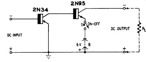
Fig. 309. High-gain power-type current amplifier.
This arrangement is shown in Fig. 309. A Sylvania 2N 34 conventional transistor is used in the input stage and a Sylvania 2N95 power transistor in the output stage. This gives a p-n-p--n-p-n type of circuit similar to the complementary-symmetry amplifier shown in Fig. 305.
The zero-signal output is 10 ma dc. An input-signal of 150 ua dc gives an output current increase of 260 ma. This represents an overall current gain of 1,670 times, or 64 db. As in the preceding circuit, maximum current amplification is obtained only with low values of external load resistance R1,. Resistances of 1 ohm or less are ideal. Proportionately lower gain is obtained with higher R1, values.
Alpha-beta conversion
Since the maximum current gain obtainable with a transistor in the common-emitter amplifier circuit is equal to beta (β, the base-to-collector amplification factor) or to alpha (a, the emitter-to-collector current amplification factor) in a common-base circuit, it is necessary to know the α and β values when designing transistorized dc amplifiers. Unfortunately, some tables of transistor characteristics list beta and some list alpha, but very few give both. However, if one factor is known, the other may be calculated. Thus:
a = 1- (1/β+1) and a/ (1-a)
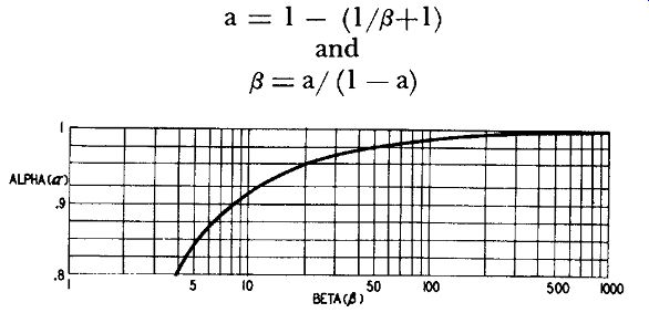
Fig. 310. Alpha-beta conversion curve.
For convenience, the graph given in Fig. 310 may be used to convert alpha to beta and vice versa. This graph saves calculations in most instances, but the curve rises so steeply at alpha values be yond about 0.991 that calculations are recommended when high accuracy is desired beyond the point at which a = 0.980 or = 100.
REFERENCES
1.Rufus P. Turner, Transistorized Voltmeter.RADIO-ELECTRONICS Magazine, December, 1954; p. 54.
2.The work leading to the design of the zero-balanced p-n-p-n-p-n circuit was performed by the author for Cornell-Dubilier Electric Corp.
8. Rufus P. Turner, Transistor Alpha-Beta Conversion. Tele Tech Sc Electronic Industries, March, 1956; p. 74.