AMAZON multi-meters discounts
AMAZON oscilloscope discounts
THE transistor has four important roles as a power supply component: (1) controlled rectifier similar to the grid-controlled vacuum-tube rectifier, (2) voltage regulator for the electronic stabilization of dc voltage, (3) constant-current converter or adaptor for converting a constant-voltage output into a constant-current output and (4) oscillator in inverter-type supplies. Transistors make possible for the first time fully electronically-regulated low-voltage dc supplies.
Because the transistor has no filament, the power supply circuits in which it can be used are considerably simplified and their power requirements markedly reduced. Its small size and freedom from heat-up time are added advantages.
Variable low-current dc power supply The transistor serves as a controlled half-wave rectifier in the circuit shown in Fig. 501. Adjustment of potentiometer R2 changes the bias applied to the base of the n-p-n transistor ( Sylvania 2N35) and this varies the dc output from zero to 10.5 volts (no-load) in response to 115 volts ac input to the filament-type transformer, T.
The curve in Fig. 502 shows the voltage regulation obtained when R2 is set for maximum dc output voltage. While this plot indicates only 50.5% regulation, this poor value imposes no difficulty since at any current level within the range the voltage may be reset to a desired level (if it has fallen off) by adjustment of potentiometer R2.
Output current drains higher than 10 ma are not recommended since this is the maximum rated collector current of the 2N35 transistor. If difficulty is experienced in covering the full output voltage range from zero to maximum, the value of the limiting resistor R1 may be changed.
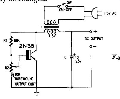
Fig. 501. Variable low-current dc power supply.
Variable high-current dc power supply
A power transistor may be substituted in the simple variable power supply to deliver higher output currents. Fig. 503 shows the circuit after the necessary changes have been made.
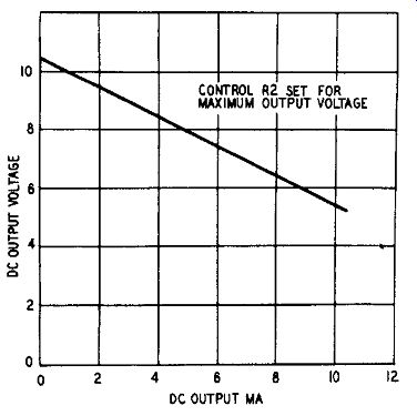
Fig. 502. Voltage regulation of low-current supply.
A Sylvania 2N95 power transistor in this circuit delivers a dc output voltage which is continuously variable between zero and 10 volts, with maximum output current up to 1.5 amperes.
At each output voltage level, the maximum current which may be drawn with safety to the transistor is limited by the maximum power dissipation rating of the transistor. For the 2N95, the maximum dissipation is 1.5 watts if the transistor is operated in free air; 4 watts when a heat sink is provided. Fig. 504 illustrates the performance limits. For example, curve A shows that at 4-volt output 0.5 ampere may be drawn safely when the transistor is operated in free air but curve B shows that 1 ampere could be drawn at this same voltage if a heat sink were provided.
A heat sink may be obtained simply by bolting the transistor solidly to an aluminum chassis (based upon chassis dimensions of 25-square-inch area and 1/16-inch thickness) . However, the transistor must be insulated electrically from the chassis by a mica separating washer (not more than 0.0005-inch thick) since the transistor case is connected internally to the collector electrode.
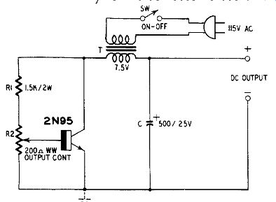
Fig. 503. Variable high-current dc power supply.
The resistance of the OUTPUT CONTROL potentiometer R2 has been changed to 200 ohms since this is the maximum external base-to emitter resistance permissible for the type 2N95 transistor.
If difficulty is experienced in covering the full output voltage range from zero to maximum, the resistance of the limiting resistor R1 may be altered.
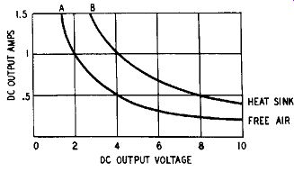
Fig. 504. Performance limits of high-current supply.
Full-wave variable dc power supply
Full-wave rectification often is preferred in a power supply be cause of its higher output current than that supplied by a half-wave circuit and the increased ease of filtering.
Fig. 505 shows the circuit of a full-wave, high-current, variable power supply which delivers twice the output current given by the
half-wave circuit described previously. Up to 3 amperes output may be obtained. The secondary of the transformer (T) may be chosen to supply up to 21 volts rms each side of center tap. This is the...
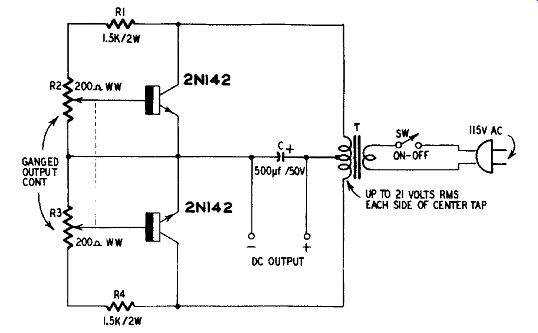
Fig. 505. Full-wave variable dc power supply.
...maximum recommended voltage since the peak value of a higher voltage will exceed the maximum permissible collector-to-emitter voltage rating of the Sylvania 2N142 power transistor employed in this circuit. When a 21-0-21-volt secondary is employed, the circuit delivers 28 volts dc output.
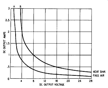
Fig. 506. Performance limits of full-wave supply.
The maximum output current which may be drawn at each dc output voltage level without exceeding the maximum power dissipation rating of the 2N142 transistor is shown by the curves in Fig.506. Curve A shows the limits when the transistors are operated in free air and curve B the limits with heat sink.
For most efficient operation, the two transistors should be matched with respect to collector current and alpha. The base voltages are varied simultaneously by adjustment of the ganged 200-ohm dual potentiometer R2-R3. If difficulty is experienced in covering the full output voltage range from zero to maximum, the resistance values of the two limiting resistors R1 and R4 may be altered.
Light-duty dc voltage regulator
Fig. 507 shows a shunt-type voltage regulator which may be added to the output of a 10-volt rectifier-filter circuit to deliver 6 volts dc regulated within 2-5% at output currents up to 10 ma. The dc output voltage is developed across the n-p-n transistor (Texas Instruments 202) .
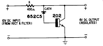
Fig. 507. Light-duty dc voltage regulator.
The control device in the circuit is the silicon junction diode (Texas Instruments 652C5) which is reverse-connected (i. e., cathode positive) . Silicon junction diodes have very high back resistance (often several hundred megohms) up to a critical reverse voltage (the Zener voltage) at which the reverse current increases suddenly to a higher value at a steep slope. This is somewhat similar to the breakdown of a gaseous diode tube. The Zener point is fixed in a given diode and provides a convenient voltage reference in applications such as voltage regulators.
In Fig. 507, the 652C5 diode has a Zener voltage of 6.0 (±5%) .
Below this point, any current flowing through the diode is negligible due to the high back resistance. When the dc output voltage rises above the. Zener point, however, the diode conducts, passing current through the base of the transistor. Because of the base-collector current amplification factor (beta) , a larger current flows in the collector circuit of the transistor and causes a corresponding voltage drop across resistor R. This voltage drop then reduces the output voltage. Output voltage regulation thus is obtained.
The output impedance of this shunt type voltage regulator circuit is approximately 25 ohms.
Heavy-duty dc voltage regulator
The preceding voltage regulator is limited to low currents and voltages by the ratings of the conventional transistor.
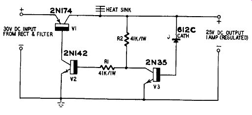
Fig. 508. Heavy-duty de voltage regulator.
Fig. 508 shows the circuit of a voltage regulator which may be added to the output of a 30-volt rectifier-filter unit to deliver a dc output of 25 volts up to 1 ampere. This is a series-type circuit pro viding better than 1% regulation at an output impedance of approximately 1 ohm.
Two power transistors V1 (Delco 2N174) and V2 ( Sylvania 2N142), one conventional transistor V3 ( Sylvania 2N35) and one silicon junction Zener reference diode D (Texas Instruments 612C) are employed. A heat sink must he provided-for transistor V1 but none is required for V2.
In this circuit, transistor V1 acts as an electronic variable resistor, introducing a controllable voltage drop in the line between the positive DC INPUT and DC OUTPUT terminals. Its resistance is controlled by varying its dc base bias. The variable bias needed for this purpose is obtained from transistor V2 which, in turn, is actuated by transistor V3 and Zener reference diode D from output-voltage changes. This is the chain through which voltage regulation is obtained. The system is sensitized by the two-stage de feedback amplifier resulting from the cascade connection of transistors V2 and V3.
A small change in dc output voltage thus is amplified sufficiently to shift the base bias of transistor V1 far enough to restore the output voltage to its original level. The 612C diode (D) is chosen for a Zener point of 25 volts.
When the 30-volt dc input is obtained from a semiconductor rectifier-filter unit (selenium, germanium or silicon), a completely tubeless heavy-duty regulated power supply results.
Light-duty constant-current adaptor
The testing of some modern electronic components (such as di odes, transistors, thermistors, varistors, tungsten filaments and other nonlinear resistors) requires a constant-current power supply. The reason for this is that in the testing (and often the operation as well) of such devices, current is the independent variable. This is the opposite condition to that of testing vacuum tubes and linear resistors where voltage is the independent variable and a constant-voltage supply is needed.
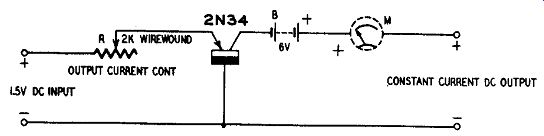
Fig. 509. Light-duty constant-current adaptor.
When using a constant-current supply, the load resistance can be varied over a wide range without materially disturbing the output-current level. The plate-cathode circuit of a pentode tube often is connected in series with a dc supply and load to obtain a constant current. The current regulation results from the constant-current plate characteristic of the pentode. (The Ep-Ip curve of a pentode is flat between widely separated limits, plate voltage changes having negligible effect upon plate current.) Fortunately, the collector ...
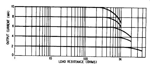
Fig. 510. Current regulation of light-duty adaptor.
... characteristic of a common-base transistor also has the pentode-like constant-current shape, a fact which suits the transistor to use as a simple tubeless constant-current adaptor.
Fig. 509 shows how a p-n-p transistor ( Sylvania 2N34) is employed to obtain constant current output from a 6-volt dc source (battery B) . The output current may be set to any desired level between zero and 10 ma (the maximum rated collector current of the 2N34) by adjusting the emitter-bias current. Emitter bias is supplied by a separate 1.5-volt source and the current level is adjusted by means of rheostat R. To read the output current value, a 0-10 dc milliammeter may be inserted in one output lead, as indicated by the symbol, M. Both the 1.5- and 6-volt potentials may be obtained from ac-operated rectifier-filter circuits, if desired.
The curves in Fig. 510 depict the current regulation afforded by the adaptor at output current levels of 2, 4, 6, 8 and 10 ma. From these plots, it is seen that the current is constant over more than three decades of load resistance values (10, 100, and 1,000 ohms) when it is 2 ma and more than two decades each (10 and 100 ohms) for higher values up to 10 ma.
To use the adaptor, first short-circuit the dc output terminals and set the current to the desired level by adjusting rheostat R. Then remove the short circuit and connect the load device to the output terminals. Refer to Fig. 510 to determine the maximum permissible value of load resistance which may be used before current regulation tails off. When testing a device requiring several test-current levels, as when plotting a family of I-E curves, vary the constant current throughout the desired range by adjustment of rheostat R.
Heavy-duty constant-current adaptor
Fig. 511 is the circuit of a constant-current adaptor operating on the same principle as the unit previously described but supplying dc output currents up to 50 ma.
CONSTANT CURRENT DC OUTPUT
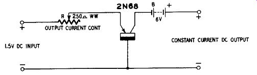
Fig. 511. Heavy-duty constant-current adaptor.
This circuit employs a p-n-p power transistor ( Sylvania 2N68) with the same 1.5- and 6-volt sources as in the preceding example.
These voltages may be obtained either from batteries, as shown, or from ac-operated rectifier-filter units. The OUTPUT CURRENT CONTROL rheostat (R) has been changed to 250 ohms in this circuit.
The curves in Fig. 512 depict the current regulation afforded by the heavy-duty adaptor at output current levels of 10, 20, 30, 40 and 50 ma.
The adaptor is used in the same manner as the light-duty unit and the operating instructions given for the latter may be followed.
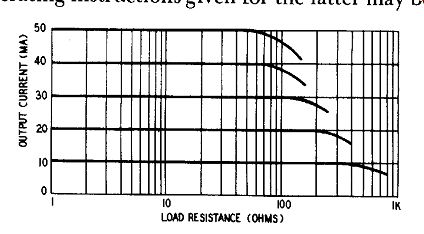
Fig. 512. Current regulation of heavy-duty adaptor.
High-voltage dc-to-dc power supply
Fig. 513 is the circuit of a compact supply operated from a small 6-volt battery and delivering from 900 to 1,000 volts dc at 5 to 10 u-a.
This unit is convenient for operating a GM tube, such as Victoreen Type 1B85, in Geiger counters. It is useful also in other low-current--high-voltage applications such as insulation testing, electro static charging, photoflash operation, oscilloscope anode supply and photomultiplier tube supply. The low operating current requirement (not exceeding 2 ma at 6 volts) permits the use of four series-connected penlight cells when extremely small size and light weight are demanded.
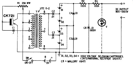
Fig. 513. High-voltage dc-to-dc power supply.
The basis of the circuit is a Hartley type oscillator employing a high-alpha p-n-p transistor (Raytheon CK721) . A portion of the primary winding (taps 1, 2 and 3) of a subminiature "ouncer" transformer (UTC type 0-2) forms the split tank coil of this oscilator. (The use of this particular transformer and the oscillator circuit configuration have been suggested by Thomas G. Knight.) The ac voltage developed across the primary (between taps 1 and 3) by the oscillator action is stepped up by the transformer and a high voltage (somewhat higher than 300 volts open-circuit) consequent ly is available across the entire secondary winding (available between taps 6 and 8, center tap 7 being unused) .
The high ac voltage is rectified and multiplied by a voltage-quadrupler circuit consisting of the four high-voltage selenium cartridges (D1, D2, D3, D4: International Rectifier Corp. type U1OHP) and the four 0.01-0 capacitors (C2, C3, C4, C5) . Filtering is provided by resistors R2 and R3 and capacitor C6. This capacitor must have a working voltage of 1,600. A satisfactory small component is the Mallory VB471 suppressor capacitor. Capacitors C2, C3, C4 and C5 must be of the mica type.
When regulation of the dc output voltage is desired, a simple method is to connect, a miniature, filament-less, corona-type regulator tube (V) such as Raytheon CK103B (900 volts) , across the output terminals, as shown by the dotted symbol. A series string of small neon lamps, such as type NE2, also can be used.
Fig. 513 shows the negative output terminal grounded. When a positive ground is desired, reverse each of the selenium cartridges ( D1 to D4) and regulator V.
The initial adjustment of the unit is simple: Connect a dc vacuum-tube voltmeter (set to its 1,000- or 1,500-volt range) to the DC OUTPUT terminals. Close switch SW and adjust rheostat RI for a dc output (as indicated by the vtvm) between 900 and 1,000 volts.
Open the switch and close it again. If the output voltage does not reappear immediately after closing the switch, readjust R1 for quick starting of the oscillator (quick buildup of dc output voltage) .