A low distortion design
by J. N. Eilis
It is recognized that to obtain low noise the usual one-transistor configuration gives generally poor results, and has a distortion level approaching 1% at about IV RMS output. The signal-to-noise ratio Can be greatly improved by using two transistors directly coupled, with the first device operating in common emitter and the second in common collector mode.
The first stage current can now be 100 uA, giving us a much better signal-to-noise ratio. This two-transistor design is often used, but suffers from latch up on overdrive.
The author's design raises the signal level from 100 mV to 1V RMS to drive a power amplifier and uses a cascode circuit to provide a more stable operating point and lower distortion. This is because the instantaneous collector voltage of the common-base transistor does not appreciably affect the current flowing in it. With a similar transistor cascode pair, the bias resistors may be low enough to inject a noise current into the lower device. Use of a complementary cascode configuration allows the selection of reasonable values of bias resistance.
To make full use of the advantages of the design (Fig. 1) the tone network is fed from an impedance equal to that presented at the output, essentially R16 and R17 in parallel. This allows a flat response when the potentiometers R19 and -R20 are mechanically central 1. The buffer stage (Tr1) allows the impedance to remain constant, independent of the volume control setting.
Component values of the tone network have been selected so that maximum bass boost or cut occurs at 50Hz, and the treble boost or cut maximum at 10kHz.
Inclusion of resistors R7, and R8 limits the treble boost or cut to only 12 dB beyond 10 kHz, as it has been found that the full 20dB (theoretical) at 20kHz is unnecessary, as the sensitivity of the ear is reducing rapidly at that point. Making R7 and R8 equal to 1 k-O allows the greater range to be obtained for the impressionist.
The frequency response is shown in Fig.2.
Without C9 the square-wave response showed slight ringing, eliminated by making C9 = 4,7pF. By increasing C9 to 10 pF the response is made 3dB down at 175kHz and the low frequency 3dB point is 5 Hz.
The design has an overall gain of 10 (20dB), and for 1 volt output with RL = 10kH and Rs = 100^ , the total harmonic distortion (measured) was less than 0.1% at 1kHz. The signal to noise ratio could not be accurately measured on the equipment available at the time, but is estimated to be -110 dB and certainly greater than -100 dB using low noise transistors --an improvement of 10 to 20dB over other designs.
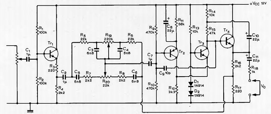
Fig. 1. Circuit diagram of tone control. Transistors Tr1, Tr3, Tr4 = BC109,
BC114, BC184. Tr2 = BC15, BC214, BC309 etc.
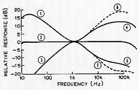
Fig. 2. Amplitude /frequency response curves of tone control circuit. 1.
Bass boost max. 2. Flat response 3. Bass cut max. 4. Treble boost max. 5.
Treble cut max. 6, 7. Treble boost and cut with R7 R, = 1-k-O.
References:
1. "Low Distortion Tone Controls", Wireless World, April 1971.
2, For example, Mullard "Transistor Audio and Radio Circuits" --Auxiliary high quality tone control.
3. Quad 33 tons control circuit.