Output stage using complementary transistors
It is only recently that matched complementary output transistors, capable of high dissipation, have been available at a reasonable price, in the past this has had the effect of concentrating high power amplifier design into two main streams.
The first uses a driver transformer with a pair of identical output transistors in a series connection. The use of a driver transformer is undesirable mainly on account of the cost, as the bandwidth of a well designed component may well extend from the sub-sonic region up to several megahertz. Nevertheless a circuit that does not require the use of such a component will obviously be at an advantage.
The alternative circuit that has been used by many designers is the quasi-complementary output stage. In this design identical output transistors are used and a complementary pair of driver transistors is arranged so as to give phase-inversion to the bases of the two output transistors. These two circuits are shown in Figs. 1(a) and 1(b) respectively. A correctly designed fully complementary output stage (Fig. 1(c) shows the basic arrangement) is capable of better performance than either of these common circuits and the reasons for this will be examined.
Compared with the quasi-complementary amplifier, the transformer-driven amplifier has the great advantage that the input impedances to the two sides of the output circuit are identical. This means that if a suitable quiescent current is used in the output transistors, cross-over distortion will be almost completely absent.
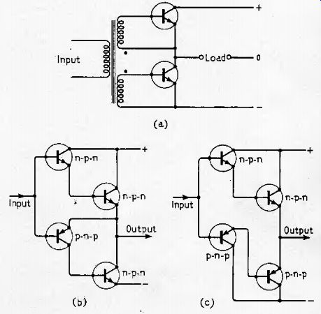
Fig. 1. Direct-coupled output stages: (a) with driver transformer: (b) quasi-complementary;
(c) fatly complementary.
---
Specification
The quasi-complementary amplifier, however, gives greater overall distortion even if identical output transistors are used.
This increase is due to the different input impedances of the two halves of the output stage in the quasi-complementary circuit.
In the upper half of Fig. 1(b) the input impedance is due to two emitter-base junctions in series, whereas in the lower half the signal feeds into only one transistor. The effect of this is an extremely marked asymmetry between the input impedances of the upper and lower halves of the output stage. Unfortunately the two input impedances cannot be equalized by the use of a series resistor as the curvature of the two stages is completely different. This dissimilarity of curvature can be seen in Figs. 2 and 3, these being the transfer characteristics of the upper and lower halves of an output stage using matched transistors.
The dissimilarity in input impedance is most marked at low values of collector current. Hence in the case of a class B output stage there is an abrupt change in slope at the cross-over point, giving rise to the well known phenomenon of cross-over distortion. This distortion may not be particularly serious when measured on an RMS basis, but as it unfortunately occurs mainly within a small part of the overall output swing, the peak value of the distortion can be surprisingly high. Also the distortion does not normally decrease appreciably as the output swing is reduced, since the effect is occurring at small signal levels. The overall effect is quite serious, therefore, and the ear seems to be very sensitive to such types of distortion.
This then is perhaps the reason why two amplifiers may sound quite different even though their 'paper' performance may be identical on the basis of normal amplifier measurements, Very few valve amplifiers suffer from cross-over distortion, and this may be the reason why the best valve amplifiers are difficult to evaluate on subjective tests. Certainly there are much greater subjective differences between the performances of current transistor amplifiers, if cross-over distortion is present it would appear that the common 0.1 percent harmonic distortion rule for an acceptable limit at peak output is no longer valid, and at least one manufacturer is working on the basis of far lower distortions being necessary.
There appear to be two ways of tackling this problem. The first is to use a larger value of overall feedback so as to reduce the effect to inaudible proportions. The main drawback with this method is that high values of overall feedback make the amplifier closer to instability, and it may be difficult, if not impossible, to achieve a reasonable stability margin. Stability may then be obtained by decreasing the cut-off frequency of a stabilizing step-network, but this has the effect of decreasing the available power at high frequencies as well as degrading the distortion characteristics at high frequencies.
Complementary Symmetry Output Stage
In view of these considerations the author decided that the best line of approach was to use a fully symmetrical output based on complementary transistors. With such a symmetrical system, there is no difference between the input impedances in the upper and lower halves of the circuit. From the basic circuit in Fig. 1(c) it will be seen that both halves of the circuit have the same input impedance characteristics because of their identical configurations. By a suitable choice of standing quiescent current, crossover distortion can be reduced to levels where it is extremely difficult to detect. This absence of cross-over distortion means that perfectly satisfactory results will be obtained if the overall distortion factor of the amplifier is similar to that commonly found in valve amplifiers, i.e. about the 0.1 percent mark. In fact lower distortions than this are possible while maintaining both unconditional load stability and good high-frequency performance.
During the development of this amplifier it was discovered that the overall performance was not as good as might have been expected from the output stage characteristics. This distortion increase was traced to the common-emitter amplifier stage that drives the output stages. This is transistor T_r3 in the complete amplifier circuit shown in Fig. 4. The effect was found to be caused by 'Early effect' [1] , the high collector voltage swing modulating the gain of the stage. In fact the overall distortion was approximately three times that which would have been expected. As this effect depends entirely on the design of the transistor in use, it was necessary to select a suitable transistor type for this position in the amplifier. This source of distortion seems to have been largely overlooked in the past, but it is obviously a possible source of extremely bad distortion. In addition, the high-frequency distortion was found to increase more rapidly than was expected and this was traced to the modulation of the collector-base capacitance of this transistor. The high collector voltage swing was causing non-linear capacitive feedback, and this in turn was increasing the high-frequency distortion. Again the only cure is by transistor selection. The type used appears to be the best currently obtainable, and the distortion introduced by these effects is below that of the output stage proper, over the whole of the audio-frequency range.
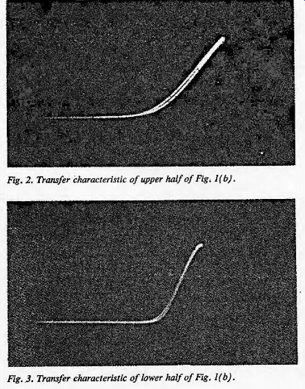
Fig. 2. Transfer characteristic of upper half of Fig. 1(b).
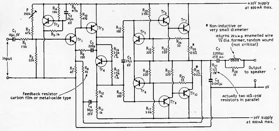
Fig. 3. Transfer characteristic of lower half of Fig. 1(b).
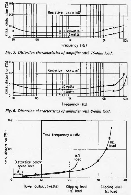
Fig. 4. Circuit of complete power amplifier. The transistors used are: Try-40361
( R.C.A.); Tr^-BC109 (Mullard); Tr3-40362 (R.C.A).; Tr3 ¦ BC107(Mullard);
Trt-BCi25 (Fairchild); Tre-~A0361 (R.C.A.); Tr1-MJ481 (Motorola); TrB--BCI26
(Fairchild); Trt-40362 (R.C.A.); Tr10-MJ49I (Motorola). Note that C7 is a
reversible electrolytic and could be made up of two 4000-p-F polarized electrolytics
connected 'back-to-back'.
Fig. 5. Distortion characteristics of amplifier with 16-ohm load.
Fig. 6. Distortion characteristics of amplifier with 8-ohm load.
Fig. 7. Variation of distortion with output power level.
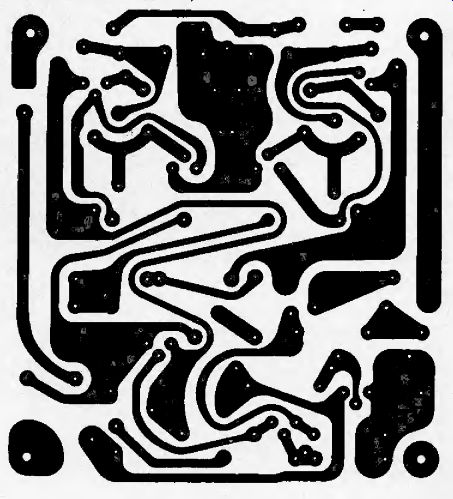
Fig. 8. Layout of suitable printed-circuit board, actual size.
For low distortion at high, frequencies, it is essential that the transistors should have as high a cut-off frequency as possible.
Planar transistors are used in all but the output stage to give this bandwidth. The output transistors used have a cut-off frequency of several megahertz and this enables low distortions to be obtained at 20 khz at full power output.
The design of the remainder of the amplifier circuit is fairly straightforward. The input stage is a common-emitter amplifier, but the. current and voltage swings associated with it are very small, so there is little difficulty in the operation of this stage.
To correct for the emitter-base voltage change of this input stage with temperature, a transistor is used to regulate the base supply current. This transistor, Tr^ operates as a rather crude temperature-sensitive zener diode and also as a hum filter. The net effect is to stabilize the DC base current of the input transistor, the supply voltage to the base of this transistor decreasing with increased temperature. This stabilization of the d.c. operating conditions enables the amplifier to deliver full output over a wide temperature range.
The bias for the driver and output transistors is produced by means of a transistor, Th,, rattler than a string of diodes as is commonly used. This is mounted in the heat sink of one of the output transistors, being as close to the output transistor as possible. This method of compensation works extremely well, and the transistor type is not critical provided a silicon one is used. The standing current in the output stage can easily be adjusted to its correct value (which is not critical) by slightly adjusting the ratio of the two resistors in the base circuit of the transistor.
For full power output from the amplifier the DC potential existing at the output of the amplifier proper should be as low as. possible. This can be adjusted by the potentiometer in the base of TVj, If this is not done the amplifier will not be able to Swing equally in the two output polarities.
The quoted figures for the amplifier were obtained using regulated supplies. Unless the amplifier is to be called on to deliver large sustained outputs, this is not really necessary. On the other hand, reduced mains voltage will severely restrict the power output of an amplifier with unregulated supplies, Commercially, a thyristor regulated supply is being utilized, and this has the two advantages of small heat dissipation and saving in components.
Constructional Points
The overall bandwidth of the amplifier is extremely wide and tire stabilizing step-network necessary only becomes operative in the ultrasonic region. Equally the inductor in series with the output lead, which improves the stability with capacitive loads, need have only a very small inductance. This wide bandwidth gives exceptional high-frequency performance as can be seen from the distortion, figures in Figs. 5, 6 and 7. Unfortunately, however, wideband amplifiers are very susceptible, to layout, particularly common coupling, leads. Provided lead lengths are kept very short there should be no difficulty, but the: author experienced tremendous variations in high-frequency stability when 'rats-nest' construction was used. For this reason the safest course is to use a printed circuit, so that the strays can be kept to a minimum. The design of a suitable board along with its component layout is shown in Figs. 8 and 9. The performance details given were measured using this particular layout. The leads to the output transistors should be as short as possible, preferably no longer than 3 to 4 inches. The size of the heat sinks for the output transistors is a matter of personal choice, the author having used sinks of finned aluminum about 4 in. by 4 in. square.
This size is not really necessary for high-fidelity use, and sinks of half this size would be adequate provided that extended periods of testing were not undertaken.
The overall performance of the amplifier is very good, considerably better in fact (on paper) than the best valve amplifiers.
Unfortunately, listening tests have shown that the performance of the amplifier is only slightly, if any, better than the best valve amplifiers. Extensive listening tests indicate only a very slight improvement in audible results, the subjective effects being almost identical. It would therefore appear that any further improvement will be of no real benefit for high-fidelity applications, the main need for work here definitely being in the field of loudspeakers, discs, etc.
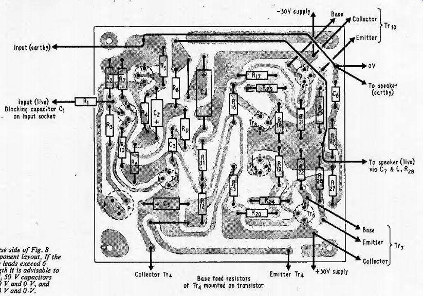
Fig. 9. Reverse side of Fig. 8 showing component layout. If the power supply
leads exceed 6 inches in length it is advisable to connect 8 uF, 50V capacitors
between +30 V and 0 V, and between -30 V and 0 V.
Owing to the absence of cross-over distortion, the distortion at low levels is very difficult to measure and the curves appear in Fig. 7. The wide bandwidth can be seen from the curves in Figs. 5 and 6, where it will be observed that the amplifier will deliver full power output from 20 Hz to 20 kHz with less than 0.1 percent of distortion. Indeed it is possible to obtain about 15 watts of power at 200 kHz. The. square-wave tests are far better than with any known valve amplifier. Even with pure capacitive loads there is no tendency whatever towards instability. The waveforms are shown in Figs. 10, 11, 12, and 13.
The protection circuits of the amplifier operate very satisfactorily, short-circuits and 50 microfarad capacitors giving no distress to the amplifier whatever. One word of caution is necessary, however; extended tests on low impedance reactive loads and short-circuits can cause high junction temperatures in the output transistors because of the finite heat-sink size. Unless one uses very large heat sinks, it is therefore undesirable to run the amplifier at full drive for extended periods when applying such abnormal load conditions, If 16-ohm load operation only is to be used, then the emitter resistors in the output stage can be increased up to 0,4 ohm, with a corresponding halving of the transistor dissipation under abnormal load conditions.
The specification is shown earlier. The overall sensitivity may be either doubled or halved by doubling or halving the value of the 1000-ohm feedback resistor. This has the effect of increasing the sensitivity at the expense of distortion if the increased amplification is felt to be necessary, With the increased feedback the overall distortion is halved, and even with this value of overall feedback the amplifier is still unconditionally load stable.
When the amplifier is operated in the reduced feedback condition for 500-millivolt sensitivity, the author cannot hear any difference in performance as compared with the halved distortion characteristic obtained with the 2-voft sensitivity. It appears therefore that no further improvement in amplifier performance will be detectable until other limiting factors are greatly improved.
In fact the author has a sneaking suspicion that this may be the end of the road so far as amplifier design for sound reproduction is concerned, further improvements being limited to power and cost,

Fig, 10, Square-wave response, 1 kHz and 8-ohm load.
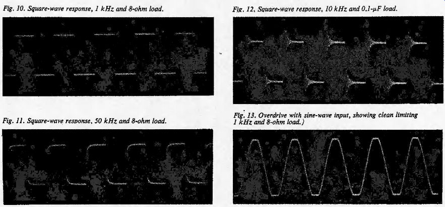
Fig. 11. Square-wave response. 50 kHz and 8-ohm load.
Fig. 12, Square-wave response, 10 kHz and 0.1-p.F load.
Fig. 13, Overdrive with sine-wave input, showing clean limiting 1 kHz and 8-ohm load.)
by Arthur R. Bailey, M.Sc., Ph.D., M.I.E.E.
Reference:
1. 'The Transistor' by E. Wolfendale. Heywood & Co., London, p. 24.
30-watt amplifier modification
Operation from a single supply rail
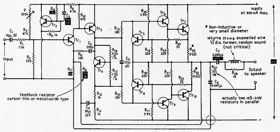
Fig. 1. Modified circuit of complete power amplifier. The transistors used
are: Tr1-40361 (R.C.A.); Trs-BCI09 (Muliard); Trz-40362 (R.C.A j; T^-BCIO?
(Mullard); Trs-BCI25 (Fairchild); Tr,-40361 ( R.C.A.); Tr^MJ4Sl (Motorola);
Tre-BC126 (Fairchild); Trt-40362 (R.C.A.): Trl0-MJ491 (Motorola). Changes
of values are indicated by black squares.
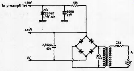
Fig. 2. A suitable power supply for the modified circuit.
The 30-watt amplifier circuit published in the May 1968 edition of Wireless fTorW utilized two power supplies and a non-polarized output capacitor. By suitable modifications to the circuit it is possible to use a single 60-volt supply rail and use a more standard polarized output capacitor. The overall cost then is appreciably reduced as compared with the original circuit. Also if it is contemplated to use a stabilized power supply, only one stabilizer has to be built.
The modifications are as follows:
1. The 0 and -30-volt amplifier connections are strapped together. This common connection goes to the negative side of the 60-V rail, and the previous +30V lead goes to the positive side of the 60-V supply.
2. The output capacitor is now a 2000 uF 50V DC electrolytic with its positive side connected to the amplifier output.
3. The feedback resistor is replaced by a 1.5-kOhm 1-W type, and its associated resistor J?, is increased to 68 ohms.
4. To maintain DC balance in the amplifier, is increased to 10 k-ohm and Rt to 22 k-ohm,
5. Owing to the changes produced in 4 above, Cs is now 10 uF and 12 volts DC working.
The d.c. conditions are now adjusted by the potentiometer R so that the amplifier side of the output capacitor C, is exactly half-way between the two supply lines in potential. The amplifier performance is not affected appreciably by these modifications if anything the overall performance is slightly better.
The design of a suitable power supply is shown in Fig. 2, The thermistor is included to prevent the charging current in the output capacitor C, becoming dangerously large at switch-on and thus endangering loudspeakers, If a stabilized supply is used, then it can be 'slugged' so as to give a slow rise in output voltage at switch-on; this making the thermistor unnecessary.
by Arthur R. Bailey, M.Sc., Ph.D., M.i.E.E,