A design using standard i.e. operationa! amplifiers to achieve a transformerless design to the specification of the British Broadcasting Corporation, who pioneered this type of level indicator.
Mono or stereo applications are catered for in the design, with separate or common meter indication. The circuit is stable against temperature and supply voltage variations, and is designed for use with a nominal 24V supply (16-30V). The main design aims were to obtain accuracy, stability, ease of law adjustment, and repeatability from one unit to another.
The peak program meter dates back some 36 years when it was developed to provide a better means of measuring line levels in sound broadcasting than that provided by normal rectifier instruments such as the VU meter. In particular the instrument was given a slow decay and fast attack time to ease reading and lessen eye strain.
Early designs were characterized by a very rapid response to transient peaks, but this was later modified since it was found that in practice the ear cannot easily detect the distortion produced by the clipping of very short duration peaks. The final attack time figure decided upon, and which is still standard, was 2.4 milliseconds. Such a response corresponds to a meter reading reaching 80% of peak using a square wave transient lasting 4 milliseconds. The decay time constant used is 1 second, which is a compromise between ease of reading and a response quick enough to record following peaks.
The graduations on the indicating meter were kept small in number and a black scale with white markings used to make for ease of reading. The basic scale division was chosen as 4dB, this being two steps of the standard B.B.C. fader controls. On a standard meter there are basically 7 divisions, with division 4 corresponding to 0-dbm on a 60012 line (0.775V RMS sine wave, 1.095V peak). The response of the peak program meter (PPM) is approximately logarithmic and the divisions on the meter are approximately evenly spaced. The extreme divisions (I to 2, and 6 to 7) represent a greater change than 4dB, namely 6dB. (Earlier meters differed in having all divisions except 1 to 2 equal to 4dB.) The present standard calibration together with the corresponding current in the meter are shown in Table 1.
The meter figures given are for B.B.C. Meter Specification ED1477, the one chosen for the design to be described.
In order to make good use of a fast charge time, the dynamic qualities of the movingcoil meter movement itself must be tightly controlled and considerably faster than that of normal movements. The meter must also be correctly damped to avoid large overshoots-two rather conflicting requirements. Whilst PPM circuits will work with standard meter movements the accuracy will be somewhat impaired unless the correct movement is used. In particular a circuit using a normal meter movement will, when set up on a standard tone level, tend to seriously underestimate short peaks on actual program material.
Table 1.
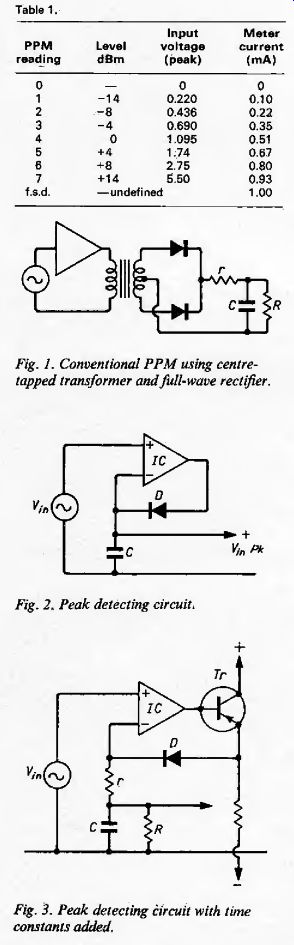
Fig. 1. Conventional PPM using centretapped transformer and full-wave rectifier.
Fig. 2. Peak detecting circuit.
Fig. 3. Peak detecting circuit with time constants added.
Peak detection
In most previous PPMs a normal full-wave rectifier has. been used, (Fig. 1), with a center tapped signal transformer; the charge and discharge time constants being controlled by the two resistors r and R. With the advent of integrated circuit operational amplifiers, however, one can now make an accurate peak rectifier without the need to use large voltage swings in order to overcome the forward drop of the rectifier, and the consequent non-linearity at low levels.
The basic circuit of such a peak detector is shown in Fig. 2. On a rising positive input, the output of the op-amp rises positively until the signal fed back to the inverting input of the op-amp via the diode D equals the level at the non-inverting input of the op-amp. When the input level falls, the diode D ceases to conduct as it becomes reverse biased, and the previous peak is stored on the capacitor C until such time as the input rises above the voltage to which the capacitor is charged, when the voltage on the capacitor again follows the input.
In practice the author has modified the basic circuit of Fig. 2 to that of Fig. 3.
Apart from the two resistors r and R, to control the charge and discharge time constants, a transistor has been added to ensure adequate charging current availability. The practical values of the components are C = 33/tF, r = 750, R = 30k-o. With such a large capacitance the peak charging current through the diode reaches approximately 100mA, which is weli above the capability of a normal i.e. op-amp, hence the additional transistor. (In practice r will be less than 75 ohm due to the necessity of allowing for the forward impedance of the diode, and other components in the 'charging' path.) The peak detector described operates only on positive peaks, whereas in a practical PPM it is necessary to measure positive and negative peaks equally, and to this end it is necessary to either (a) have a similar peak detector of reversed polarity to detect the negative peaks or (b) to have a second similar peak detector and precede it with a unity gain phase inverter.
It was decided to take the second course since it allowed the two positive peak detectors to be combined, sharing a common capacitor, charge and discharge resistors.
In this way the highest peak from either detector will automatically be selected.
The unity gain inverter can of course be a center tapped transformer as in previous PPMs, or else another op-amp connected as a unity gain inverter, as shown in Fig. 4.
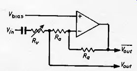
Fig. 4. Unity gain inverting circuit.
Provided that the loading on the two outputs is small, both the a.c. and DC levels will be equal except for the phasing.
Since the input to the two peak detectors is the non-inverting input of two op-amps the loading is in fact quite low. The difference of DC level due to the unequal base supply resistances of the two peak detectors is approximately equal to the typical offsets of the i.es, and is therefore fairly negligible when compared to the signal levels, i.e. they are less than 10% of the lowest division (1 on the PPM = 0.22V pk). In addition there is a zero set control on the output amplifier which can largely remove the effect from the meter deflection.
Gain adjustment is achieved by the single control Ry for both peak detectors. Whatever the value of Rv, Voia and 1%, (Fig. 4) will remain equal and opposite to one another so far as signal excursions are concerned, although at the same DC level.
Law corrected output amplifier
The voltage across the peak storage capacitor is applied to a law corrected summing amplifier, whose input resistance (and hence the discharge time constant) will be set by an input resistor Rx to the summing point.
The basic principle of this amplifier is illustrated in simplified form in Fig. 5.
The initial gain for voltages close to the bias voltage line ( that is from 0-3 on the PPM scale, is linear, and is set by the ratio Ri./Rx since for small output levels the transistor 7% is reverse biased. When the emitter potential of TV-! falls below its bias voltage F1 the additional feedback
resistor Rfi is brought into operation in parallel with Ry so that the gain is reduced to
Ry ' Rfi RJJ<y+RIt)
Further feedback resistors Rf2-RfA together with transistors Tr2-Tr4 each controlled by bias voltages V2-V4 respectively, are similarly connected to the amplifier to successively reduce the gain with increasing negative output level. The law corrected amplifier therefore approximates the desired curve of input versus output with a five section linear gain curve as shown in Fig. 6. The choice of feedback resistors and bias voltages is made to get the best match to the actual smooth curve. In practice this was done by graphical methods together with calculation. The values were finally adjusted by trial and error to get the best result, together with the use of standard E24 values. The choice of values possible is almost infinite depending on the choice of break points.
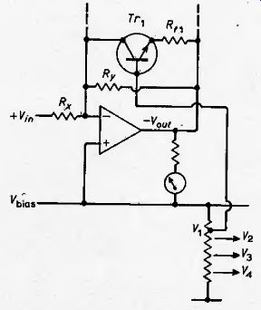
Fig. 5. Use of a transistor in the feedback path to provide law correction
of transfer characteristic.

Fig. 6. Low corrected transfer curve approximated by a five section linear
characteristic.
Complete practical circuit
Fig. 7 shows the complete circuit of the peak program meter based on the circuits described above. It is designed to work with a IraAmeter movement to B.B.C. Specification ED 1477, There are a few items in this circuit not covered in the above circuit descriptions.
First, in the feedback network of the law corrected amplifier a diode has been added to prevent any appreciable positive excursion of the amplifier's output on switching on or off. Secondly, a zero set potentiometer is added to this amplifier to take out the combined zero errors of the four opamps which although small enough to hardly affect the working accuracy is nevertheless rather annoying visually in the absence of an input level.
The zero set potentiometer is the usual value for the type 741 op-amp but is connected in a somewhat different manner.
Instead of being connected between the two offset points of the 741 and the negative supply line, a resistor is connected to the slider of the potentiometer and returned instead to the 9.1V bias line. This arrangement allows a much wider range of adjustment than the usual connection, which although adequate to cope with the offset of one 741 op-amp is not sufficient to cope with the combined offset of four op-amps if these should unfortunately be additive.
The DC operating level of all stages is determined by the bias supply of + 9.1V stabilized by the zener diode /L which also supplies the bias chain for the output amplifier's feedback network. This bias chain has an overall adjustment in order that the exact law correction of the completed instrument may be set up, and the tolerances of the various elements allowed for-in particular that of the zener diode stabilized voltage.
The 1mA meter to B.B.C. Specification ED 147 7, has a resistance of 600D ±5% so that with its series resistor of 4.7k-ohm (R15), full-scale deflection corresponds to -5.3V with respect to the T-9.1-volt bias line.
Maximum overdrive of the meter is limited therefore to a little less than the bias line voltage, or approximately some 8V, corresponding to roughly 150% overdrive-a reasonable value for meter protection. The general action of the circuit normally prevents reverse deflection, but in any case the diode in the feedback circuit prevents more than 0.6V being applied to the meter, corresponding to -11% deflection.
Due to the very high peak currents occurring in the peak rectifier circuit, particularly in the collector currents of TV, and 7>2, some measure of isolation from other equipment sharing the same supply line is necessary, To this end decoupling by jRjj and C3 is provided.
A resistor of 620fl is included so that, it can be linked into circuit to give a line terminating impedance of 600-ohm instead of the normal line bridging input impedance of around 16kfl.
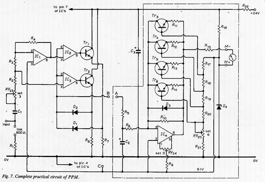
Fig. 7. Complete practical circuit of PPM.
Setting-up and performance
The procedure for setting-up the PPM is a simple one. First, with zero input voltage, the zero is set ('Set 0' control) RV2^. Next a level corresponding to --4dBm (reading 3 on the PPM scale) or 490rnV RMS sine wave, 690mV peak, is applied and the
'Set 3' control (-RF^s) is adjusted to bring the meter pointer to. 3 on the scale. Finally a level of + 8dBm, (reading 6 on the PPM scale) or 1.94V RMS sine wave (2.75V peak), is applied to the input and the 'Set 6' control TJFjj is adjusted to bring the meter pointer to 6 on the scale. The meter is then checked at 0, 1, 2, 3, 4, 5, 6, 7, and f.s.d. points as listed in Table 1 , and any small adjustment made to the 'Set' 0, 3, and 6 controls to minimize the spread of enors.
Having completed the sequence of adjustments the meter should read within ():5dB at 1kHz at all scale marks, although f.s.d, is as stated in Table 1 undefined (it will usually correspond to around 5.3V RMS sine wave). Performance versus temperature. The PPM has very little variation with temperature.
A 30 degree C rise in temperature (from 17 deg. C) gave only about 10 uA change in meter current at any point of the scale, i.e. about 1 % of f.s.d.
Performance versus frequency. As shown in Fig. 8 there is a slight droop in the upper frequency range, and this is due to the limited slew rate capability of the 741 opamp in the peak detectors. Amplifiers having a higher slew rate have been tested and do remove this limitation in the audio range. The 748 op-amp has a higher speed performance than the 741 but uses external compensation; this allows the response to be tailored to suit any particular need.
Fig, 9 shows how two 748 op-amps may be used for IC2 and /C3, together with appropriate extra components to obtain a flat frequency response over the whole audio band. There is still a slight fall off at 20kHz but this is greatly reduced as compared to the 741 op-amp.
In practice does this HF droop matter? The author would argue that for the monitoring of practical speech and music levels it does not matter to any noticeable extent. This is because of two factors.
First, there is the attack response time of 2.5ms used in the circuit, meaning that a level must last for several milliseconds to register near to its true peak level, and secondly, in general, frequencies above about 5kHz do not exist at as high a level as the lower frequencies, and these lower frequencies therefore largely, determine the peak amplitude at any time.
Performance versus supply voltage. Over the range of 16 to 30V there is little visible change of reading at any level of input. The circuit is designed for operation from a nominal 24-volt supply. Supply current is somewhat dependent on input level, and is typically MmA at zero input, rises fairly rapidly as input is applied, and reaches 20mA at full scale. There will be some variation from unit to unit but at 24V (he current should remain in the limits 1322niA. The current demand is also dependent on supply voltage being lowest at i6V and highest at 30V. An absolute maximum supply voltage of 36V should never be exceeded.
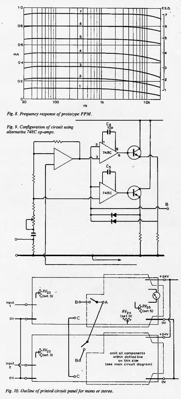
Fig. 8. Frequency response of prototype PPM.
Fig. 9. Configuration of circuit using alternative 748C op-amps.
Fig. 10. Outline of printed circuit panel for mono or stereo.
Connections for stereo use with a single common meter
For economic or space reasons, it may be desired to use two PPM circuits with a common meter, and the printed circuits were designed with this in mind as an option. The method of interconnection is shown in Fig. iO where two input circuits up to point B are used, with only one output circuit from point A onwards. The bias supply is made common to both boards by finking points C together.
To set up the meters in this method of connection the zero is first set at nil input level (to both inputs), 'Set 0' control (R V2). Next inputs of --4dBm are connected to each input in turn and the appropriate
'Set 3' control {RV13) for that channel is set to give a reading of 3 on the PPM. Finally the 'Set 6' control is set to give a reading of 6. from either input at a level of +8dBm.
For the setting of the 'Set 3' and 'Set 6' controls both inputs may be connected in parallel and the switches shown in Fig. 10 operated to select the channel to be set up.
The dotted lines in Fig. 7 show the section of circuit omitted on one board and correspond to the dotted lines in Fig. 10,
Acknowledgements
The author wishes to express his grateful thanks to the 11. B.C.'. Engineering Department and in particular to Mr. A, E. Tolladay, for considerable help and encouragement, also to Ernest Turner Electrical Instruments Ltd. for their help in the project.
Constructional appendix
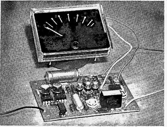
The circuit is built on a printed circuit board 3^x 3^ inches in size with mounting centres of 3.1 x2.! inches (6BA). The board, which is suitable for either the circuit with 741s in all stages or the higher speed circuit with 748s in the peak rectification stages, is shown in prototype form in the photograph.
Layout of production boards will differ slightly but all component positions are silk screened onto the component side of the board.
It is essential that the charge storage capacitor C1 be a low leakage type, hence the specification of a solid dielectric tantalum type. An alternative is the solid dielectric aluminum capacitor such as Mullard type 121 15339 (33^F 16V) or 121 16339 (33/tF 25V). However, it should be remembered that these are of 20% selection tolerance, and it may be necessary to select one to the necessary tolerance of 10%. In general normal aluminum electrolytics are not suitable, due to their high leakage (especially at elevated temperature) and very wide tolerance, even of the higher quality typ (e.g. Multard C428 is -10 +50%), No special techniques are used in the con struction and the only precautions neede are to ensure correct insertion of the 8-pi dual-in-line op-amp packages, and to avoi shorts on the board due to careless solderin (a miniature soldering iron is, these days essential for printed circuit work). Mountin pads are used under the 6 transistors bu are not absolutely essential. Connection are by 14-0076 p.v.c, covered leads a shown in the photograph.
All component parts in kit form togethe with Ernest Turner PPM meters type 64 are available from Key Electronics, P.O Box No. 7, Bournemouth, BH7 7BS, Hants
---- Components list
All the above are 3% metal oxide or metal film (e.g. Welwyn MRS or Electrosi! TR5).
* Resistor R21 will normally be a wire link.
(For use only where a higher reference line voltage than 9.1V is to be used.)
N.B. The TO-99 versions (multi-lead TO-5), of the 741 and 748 may also be used since they have the same lead layout and are easily arranged in d.i.l. lead configuration. Jermyn Industries Ltd., type MON-8L mounting pad may be used to achieve this end.
Preset potentiometers py^ PV2i 10k ±20% R%5 5k ±20%
Open cermet potentiometers (R.S, Components or A.B. Electronic Components). Semi-sealed type Morganite 81E may also be fitted (also from R.S. Components).
by L. Nelson-Jones, F.I.E.R.E.
-----