The high-gain and wide passband of the operational amplifier-type IC enable this device to operate as an oscillator over a wide frequency range. The IC oscillates readily when feedback is applied to its noninverting input and adjusted to the proper amplitude.
The IC is especially useful in resistance-capacitance-tuned oscillators, since its overall gain is more than adequate to offset the attenuation of the RC network. Also, the dual input of the differential IC permits not only positive feedback (for oscillation), but also negative feedback in some circuits (for improving the output waveform). This section describes seven IC oscillators-three RC arrangements, three LC arrangements, and one crystal arrangement. These are generalized circuits that may be used with practically any high-gain operational-amplifier IC. Specific terminal designations therefore are not given except for inverting input, noninverting input, input ground (common), and output. De supply connections are not shown, since these (and the particular Vee and Vee voltage values) will vary with the individual IC. Where possible, as much practical operating information as practicable is given for these general illustrations.
1. TWIN-T RC AF OSCILLATOR
Fig. 1 shows the circuit of a resistance-capacitance tuned AF oscillator employing a twin-T null network (C1-C2 C3-R2-R3-R4) to determine the frequency. The IC should have a voltage gain of 60 dB.
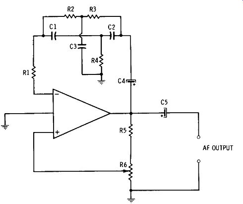
Fig. 1. Twin-T RC AF oscillator.
This arrangement is essentially a sharply tuned AF amplifier to which positive feedback has been added for oscillation.
The twin-T network is inserted in the negative-feedback loop, and being a null network it removes one frequency (fr) from the negative feedback. The IC gain accordingly is cancelled at all other frequencies, while fr is readily trans mitted. In the network, the following formulas apply:
where,
C's are in farads, R's are in ohms, fr is in hertz.
C1= C2 = ½C3
R2 = R3 = 2R4
fr= 1/ (2 pi R2 C1)
Coupling capacitor C4 serves as DC blocking, and its capacitance is very high with respect to C1, C2, and C3. It accordingly does not affect fr. Resistance R1 is high with respect to the input impedance of the IC, and serves to minimize loading of the twin-T network by the IC input circuit.
The addition of positive feedback, through the signal divider R5-R6, causes this sharply tuned amplifier to oscillate at frequency fr. When potentiometer R6 is set to the point at which the circuit just begins to oscillate, the output-signal distortion is very low.
The oscillator may be made continuously tunable (e.g., 20 Hz to 20 kHz) by substituting a 3-gang potentiometer for resistors R2, R3, and R4, and switching capacitors C1, C2, and C3 in trios to change bands. Output control may be obtained with a potentiometer either added to the output or inserted between stages of the IC.
2. PHASE-SHIFT RC AF OSCILLATOR
The phase-shift type of resistance-capacitance-tuned AF oscillator is well known for its very low harmonic distortion.
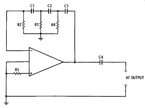
Fig. 2. Phase-shift RC AF oscillator.
In this type of oscillator, RC tuning is accomplished with a 180-degree phase-shift network connected in the feedback loop of an inverting amplifier. The network accordingly produces the correct phase rotation of the signal for oscillation.
Fig. 2 shows the connections for a phase-shift-type IC oscillator.
In this arrangement, the phase shift network consists of three identical RC legs in cascade: C1-R2, C2-R3, and C3-R4.
Here, C1= C2 = C3, and R2 = R3 = R4.
Each of these legs introduces 60 degrees of phase shift. The frequency at which the total shift is 180 degrees is found by the following formula: where, fr is in hertz, R2 is in ohms, C1 is in farads.
fr= 1/ (10.88 R2 C1)
In order to offset the inherent attenuation of the RC net work, the gain of the IC should be 40 dB. The noninverting input of the IC is not used in this arrangement, it being re turned to ground through resistor R1 ( usually of the order of 1000 ohms).
This oscillator might be made continuously tunable ( e.g., 20 Hz to 20 kHz) by substituting a 3-gang potentiometer for resistors R2, R3, and R4, and switching capacitors C1, C2, and C3 in trios to change bands. However, the attenuation of the network increases as the resistances decrease, and this would cause the output-signal amplitude to decrease rapidly with frequency, and oscillation might even cease when R2, R3, and R4 become very small at the high frequencies. Output control may be obtained with a potentiometer either added to the output or inserted between stages of the IC.
3. WIEN-BRIDGE RC AF OSCILLATOR
Whereas the resistance-capacitance-tuned AF oscillators described in the preceding sections require three resistances and three capacitances for tuning, the IC circuit shown in Fig. 3 needs only two resistances (R1 and R2) and two capacitances (C1 and C2). The C1-C2-R1-R2 combination is half of a Wien bridge which, like the twin-T network in Fig. 1, is frequency sensitive.
The RC circuit is connected in the positive-feedback loop (to the noninverting input terminal). In the network, C1= C2, R1 = R2, and the response frequency is found by the following formula:
…where, fr is in hertz, R1 is in ohms, C1 is in farads.
fr= 1/ (2 pi R1C1)
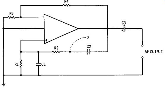
Fig. 3. Wien-bridge RC AF oscillator.
Negative feedback is applied through resistors R3 and R4 (which form a signal voltage divider) to the inverting input terminal. This negative feedback lowers output-signal distortion; however, it must be proportioned correctly (through adjustment of R3 and R4) so that it does not cancel the positive feedback and thus kill oscillation.
Oscillators of this type are readily made continuously tunable (e. g., 20 Hz to 1 MHz) by substituting a 2-gang potentiometer for resistors R1 and R2, and switching capacitors C1 and C2 in pairs to change frequency bands. When the oscillator is tuned over a wide frequency range, however, its output-signal amplitude tends to vary with frequency.
But this variation may be minimized by means of a suitable nonlinear resistor, such as a thermistor, varistor, or double ended zener diode, connected between point "X" and ground.
Output control may be obtained with a potentiometer either added to the output or inserted between stages of the IC.
4. TRANSFORMER-FEEDBACK AF OSCILLATOR
Fig. 4 shows the connections for a simple AF oscillator in which a miniature audio transformer (T1) supplies both the feedback and the tuning that convert the IC into an oscillator. A low-gain IC will operate successfully in this circuit.
In this arrangement, positive feedback is supplied to the noninverting input of the IC through transformer T1, which may be any convenient small unit. The frequency of oscillation is determined by capacitance C1 and the inductance (L) of the transformer winding across which this capacitor is connected. The following formulas apply to Fig. 4: where, fr is in hertz, L is in henrys, C1 is in farads.
C1 = 1/ ( 417"2f2L) L = 1/ ( 41r2f2 C1)
fr=l/(2~)
The transformer must be phased correctly for oscillation; but in the absence of oscillation due to incorrect wiring, the connections to only one winding need be reversed.
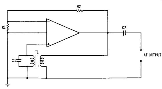
Fig. 4. Transformer-feedback AF oscillator.
Negative feedback is applied through resistors R1 and R2, which form a signal-voltage divider, to the inverting input terminal. This negative feedback lowers output-signal distortion; however, it must be proportioned correctly (through adjustment of R1 and R2) so that it does not cancel the positive feedback and thus kill oscillation.
Output control may be obtained with a potentiometer either added to the output or inserted between stages of the IC.
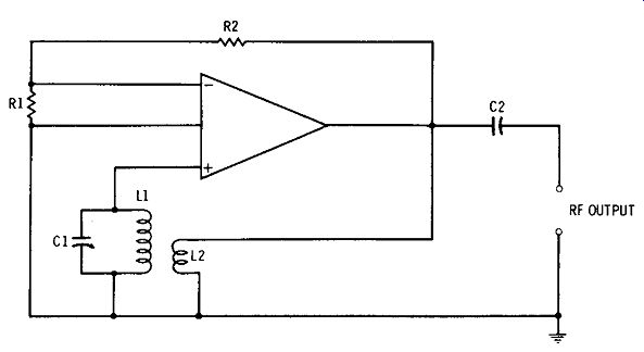
Fig. 5. Transformer-feedback RF oscillator.
5. TRANSFORMER-FEEDBACK RF OSCILLATOR
The radio-frequency oscillator circuit shown in Fig. 5 is similar to the transformer-feedback AF oscillator described in Section 3.4, except that in this RF oscillator, positive feed back (for oscillation) and tuning are provided by an air-core transformer, L1-L2. A low-gain IC will operate successfully in this circuit.
In this arrangement, positive feedback is supplied to the noninverting input through the L1-L2 combination. (L1 is the high-turns winding of the transformer, whereas L2 consists of approximately one-quarter of the turns in L1 and is closely, but not tightly, coupled to L1.) The frequency of oscillation is determined by capacitance C1 and inductance L1. This frequency fr is found by the following formulas:
where, C1 = 1/ ( 4 pi^2 f2 L1)
L1 = 1/(4 pi ^2 f^2 C1)
fr= 1/ (2 pi __/L1C1)
C1 is in picofarads, L1 is in microhenrys, fr is in megahertz.
The transformer must be phased correctly for oscillation; but in the absence of oscillation, due to incorrect wiring, the connections to only one winding need be reversed.
Negative feedback is applied through resistors R1 and R2, which form a signal-voltage divider, to the inverting input terminal. This negative feedback stabilizes operation and reduces output-signal distortion; however, it must be pro portioned correctly (through adjustment of R1 and R2) so that it does not cancel the positive feedback and thus kill oscillation.
Continuous tuning is provided by variable capacitor C1.
For wide-range coverage, L1 and L2 may be changed in pairs to switch frequency bands.
6. COMBINATION AF/RF OSCILLATOR
Fig. 6 shows the connections for an oscillator that, by means of plug-in inductors and plug-in capacitors, may be used to generate either audio-frequency or radio-frequency signals over a wide frequency range. In this arrangement, both positive and negative feedback are employed.
The tuned circuit (L1-C1) that determines the frequency of oscillation is connected in the negative-feedback loop. Acting as a wavetrap, therefore, this tuned circuit removes its resonant frequency, fr, from the feedback. The IC, acting accordingly as a sharply tuned amplifier, thus transmits fr, but has its gain cancelled at all other frequencies. The positive feedback, obtained through the signal voltage divider R1-R2, then causes the circuit to oscillate at frequency fr, The formulas for this circuit are: where, fr is in hertz, L1 is in henrys, C1 is in farads.
C1 = 1/ ( 4 pi^2 f^2 L1)
L1 = 1/ ( 4 pi^2 f^2 C1)
fr= 1/ ( 2 pi __/L1C1)
High capacitance and inductance combinations will generate audio frequencies, and low capacitance and inductance will generate radio frequencies.
The intensity of oscillation depends upon the setting of positive-feedback potentiometer R2, so some degree of out put-signal amplitude control is possible with this potentiometer. The circuit will operate with a variety of ICs.
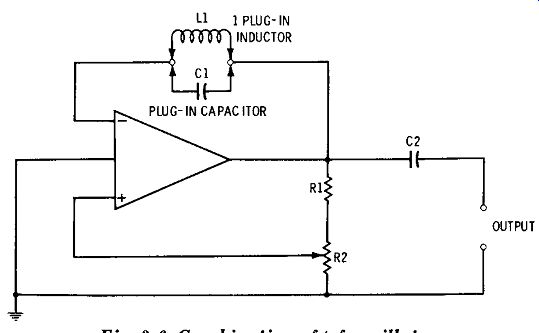
Fig. 6. Combination AF /RF oscillator.
Since output-coupling capacitor C2 must transmit low and high frequencies, its capacitance must be a compromise value, such as 0.01 µF, unless the user is willing to change this capacitor along with L1 and C1.
7. CRYSTAL-CONTROLLED RF OSCILLATOR
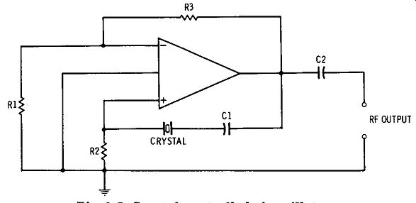
Fig. 7. Crystal-controlled RF oscillator.
Fig. 7 shows the connections for a crystal-controlled RF oscillator requiring no tuning. This arrangement will work with multistage ICs of all sensitivities; however, medium and high-gain units are recommended.
In this circuit, the crystal (XTAL) acts as an extremely high-Q bandpass filter in the positive-feedback loop of the IC. Positive-feedback current passed by the crystal develops a voltage drop across resistor R2, and this voltage is applied to the noninverting input terminal of the IC. Oscillation thus occurs at the crystal frequency. Capacitor C1 serves only for de-blocking, its capacitance being selected for low reactance at the crystal frequency. The input-ground (common) terminal of the IC is returned directly to the circuit ground, as shown.
A negative-feedback loop also is provided. This consists of resistors R1 and R3, which form a signal voltage divider.
Negative-feedback current through this divider develops a voltage drop across resistor R1, and this voltage is applied to the inverting input terminal of the IC. The amplitude of this voltage must be correctly set (by adjustment of resistors R1 and R3) so that it does not cancel the positive feedback and thus kill oscillation. The negative feedback improves stability and lowers output-signal distortion. However, it may be dispensed with entirely when high harmonic output is desired, as in some transmitter service.