AMAZON multi-meters discounts AMAZON oscilloscope discounts
Introduction:
Some of the circuit techniques which are useful in the design of amplifiers for low frequency signals have been examined in Section 6, and while most of the circuit layouts which work at low frequencies will also work at higher ones, they don’t generally work as well, and there is nearly always a problem in obtaining a useful stage gain from simple circuitry at high frequencies. This leads to practical difficulties, particularly with small signals, in getting a good enough overall signal to noise ratio, bearing in mind that every amplifier stage will introduce some additional circuit and device noise of its own. It’s therefore essential to ensure that the individual stage gains --especially at the front end of an amplifier -- are sufficiently high that the amplified noise at their inputs will always be greater than that generated by following stages.
The use of a resonant tuned circuit, of the kind analyzed in Section 11, is a great help in this respect since the voltage magnification given by the Q of such a circuit will provide an almost noise-free element of gain, so that the 'gain' stage may only be needed to act as an impedance transforming 'buffer' to convert the high output impedance of a parallel resonant tuned circuit into a low impedance signal source which can drive following stages. However, this approach is only useful if amplification at a single frequency, or a narrow band of frequencies, is acceptable. This was almost always the case in early radio receivers, where the main task of the 'radio frequency' (RF) amplifier stage was just to increase the size of the received signal, from the aerial input, to a level where a simple rectifying device could perform the function of separating the modulation from the radio frequency 'carrier'. The RF stage might also give a useful increase in selectivity to help the user to separate a wanted signal from another on an adjacent carrier frequency.
Practical circuitry
In the early days of radio, when triode valves were the only types available, such a 'tuned' RF amplifier stage would use the type of circuit layout shown schematically in FIG 1, using both an input and an output tuned circuit. However, this arrangement suffers from the snag that when these two LC circuits are nearly in tune, the circuit will almost inevitably burst into oscillation. This problem can be mitigated if the tuned circuits are fairly heavily damped by the parallel connection of suitable value resistors, but this will then reduce the effectiveness of the tuned circuits, in respect of the gain and selectivity which they could provide. This instability occurs because the small anode/grid 'stray capacitance' (C_fb), will allow the unwanted feedback of energy from the amplified signal at the valve anode into the input tuned circuit: a problem which will worsen as the operating frequency is increased, because this will also reduce the RF impedance of the stray capacitance feedback path.
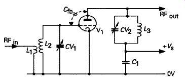
FIG1 Typical triode valve RF amplifier stage.
The first part of the requirement for continuous oscillation, that the loop gain should exceed unity, will be met when the impedance of the feedback capacitance, at the frequency in question, is less than or equal to the product of the dynamic impedance of the input tuned circuit and the voltage gain of the stage. The second part of this requirement, that the feedback voltage should be exactly in phase with the input signal at the frequency at which oscillation will occur, will be satisfied at some frequency near the frequency of resonance, because of the combined effect of the phase shift in the signal passing through the feedback capacitance and the additional, and quite abrupt, phase shift in an LC tuned circuit, illustrated in FIG 2, between its output voltage and input current, when the input signal passes through its resonant frequency.
Although it appears possible to tune the input and output circuits so that oscillation is avoided, this is, in practice, very difficult to achieve. This means that practical triode RF amplifiers must use either a gain stage of the kind shown in FIG3, in which the effect of the feedback capacitance is neutralized, or a 'grounded grid' type layout, of the kind shown in FIG4.
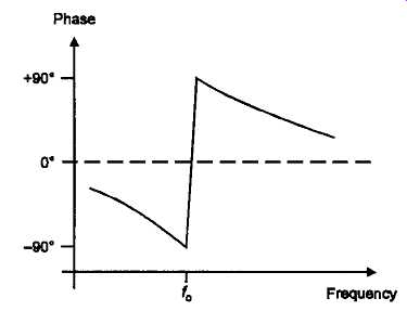
FIG 2 Phase angle of tuned circuit as a function of applied signal frequency
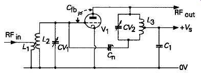
FIG 3 Neutralized triode valve RF amplifier stage
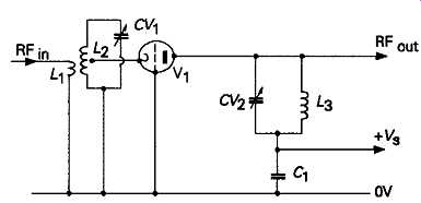
FIG 4 Grounded grid RF amplifier stage
In the circuit of FIG3, the mid-point of the output tuned circuit is earthed at RF, so that a signal which is in antiphase to that at the valve anode is developed at the opposite end of the LC circuit, and this allows the deliberate feedback, through the neutralizing capacitor (Cn), of a signal which can exactly cancel that arising from the internal feedback due to the valve stray capacitances (C_fb). This arrangement works quite well, but demands a tapped output coil, and also prevents the use of a ganged tuning capacitor, since the rotor of the tuning capacitor ,C, cannot now be taken to a point of zero RF potential. It’s also, in practice, rather a tiresome task to set Cn to a value which will eliminate the tendency to oscillation over the whole required operating frequency range.
The grounded grid amplifier stage of FIG 4, which uses the grid electrode of a triode valve as an electrostatic screen between the input and output tuned circuits, works very well, and is often found, in a 'solid-state' version, as the RF gain stage in inexpensive FM radio circuits, where a bipolar transistor is used in a layout of the kind shown in FIG5. The description 'grounded base' is normally used for this type of circuit.
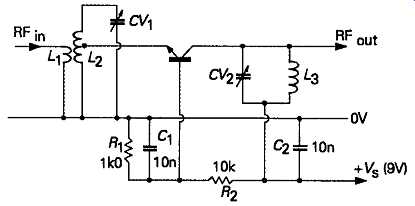
FIG 5 Transistor operated grounded base RF amplifier stage.
The only problem with either of these last two circuits is that both the cathode circuit of a valve and the emitter circuit of a transistor are very low impedance points, because of the effect of internal negative feedback. This means that the input to the gain stage must be taken at a tapping point low down on L2 to provide a low enough drive impedance, and this limits the voltage gain available from the input tuned circuit, L_2/CV_1.
In the case of valve amplifiers, an engineering solution to the problem of unwanted feedback from anode to grid, due to inter-electrode stray capacitances, was provided by the introduction of a 'screen grid', connected to a suitable low RF impedance positive potential, and mounted internally between the grid and the anode. Such screened grid valves, and their later 'RF pentode' successors, solved the problem of internal capacitative feedback very satisfactorily, and allowed a useful degree of amplification to be obtained up to frequencies at which the loss of efficiency due to electron transit times within the valve, and to the parasitic inductance of the connections to the valve from its holder, began to be a significant factor.
The contemporary solid-state equivalent to the screened grid valve is the dual gate MOSFET, shown symbolically in FIG6. In this type of device a second insulated gate electrode metallization (G2), is formed on the FET channel between the signal gate (G1), and the drain. With contemporary dual gate MOSFETs, feedback capacitances of 0.01pF, or less, are attainable; as compared with the 3-10pF collector-base capacitance of a typical small-signal bipolar junction transistor, or the similar drain-gate capacitance of a typical junction field effect device; and this allows stable RF amplification, using a straightforward gain stage, of the kind shown in FIG7, up to several hundred megahertz. Recent dual-gate MOS FETs based on gallium arsenide, rather than silicon, have extended the usable frequency range up to the GHz region.
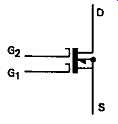
FIG 6 Dual-gate MOS-FET RF amplifier device.
FIG 7 Dual-gate MOS-FET RF amplifier stage.
Unfortunately, the high circuit impedances associated with MOSFETs lead to a somewhat worse circuit noise figure in comparison with gain stages based on bipolar junction transistors or junction FETs. Circuit arrangements using standard devices which avoid the problem of feedback capacitance by virtue of the circuit layout are the long tailed pair layout shown, for bipolar junction transistors, in FIG8, and the cascode layout shown in FIG9, using junction FETs. In these cases the output transistor is driven by either its emitter or its source, so the base or gate -- which is taken to a low impedance point in respect of RF -- is interposed between the input and output of the amplifying device. This gives a similar degree of input-output isolation to the grounded-base circuit shown in FIG5, but with a higher input impedance. Both of these circuit layouts allow stable gain to be obtained up to quite high operating frequencies.
FIG 8 Long-tailed pair RF amplifier stage RF
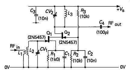
FIG 9 Cascode connected FET amplifier stage
An interesting version of the cascode circuit which combines the characteristics of both of these layouts, by the use of complementary symmetry devices, is shown in FIG 10. This arrangement gives the isolation of the grounded-base stage as well as the high input impedance associated with an emitter follower.
In both the cascode and the grounded-base layouts the current through the output device is almost entirely determined by the emitter/base forward potential. This gives rise to the type of relationship between collector current and collector/base voltage shown in FIG11, in which the actual collector voltage has very little influence on collector current, which means that the device has an exceedingly high dynamic output impedance. This is useful since such a stage can be connected directly to a parallel resonant tuned circuit without introducing significant parallel resistance damping of its characteristics.
FIG 10 Complementary cascode RF amplifier stage
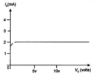
FIG 11 Cascode collector current characteristics
Both MOSFETs and junction FETs have very high input impedances (>1000), and can therefore be connected directly across an LC tuned circuit, as shown in FIG9, without lowering its Q -- its voltage magnification factor -- whereas a bipolar device would nearly always require that it should be driven from a tapping point rather lower down on the tuned circuit to lessen the effect of its relatively low (5-10k Ohm), input resistance on the Q of the circuit.
An ingenious alternative method of neutralizing an RF gain stage -- in this case a junction FET, chosen because its nearly ideal 'square law' transfer characteristics give low cross-modulation between wanted and interfering input signals -- is described by Philips (Electronic Components and Applications, May 1980), and shown in the circuit of FIG12. In this, the tuning capacitor of the input tuned circuit (CV1), is connected effectively between gate and source, and a small inductor, in this case of ???? inductance, is connected between the source and the 0V line.
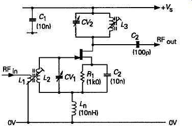
FIG 12 Source inductor neutralization circuit
Where ceramic SAW filters (see Section 11), are to be used as selectivity elements, they usually require an input and output load impedance of the order of a few hundreds of ohms. At this sort of impedance level a standard bipolar transistor operated feedback amplifier, such as the circuit shown in FIG 13, which I designed for an FM tuner IF stage, provides quite a satisfactory answer. In the case of the circuit illustrated, the amplifier provides a stable gain of approximately 50dB at 10.7MHz. Allowing for the anticipated 28dB loss in the four SAW filters this meets the design value for the residual IF gain of 22dB ( 5).
Bandwidth, noise and cross-modulation
For any given source impedance, ambient temperature and measurement bandwidth there will be an associated thermal noise voltage (En), defined by the equation:
…where k is Boltzmann's constant (1.38x10 is the circuit impedance, T is the ambient temperature in °Kelvin (the so-called 'absolute temperature', based on a zero of -273.3°C) and B is the measurement bandwidth, in Hz.
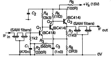
FIG 13 FM receiver IF amplifier for use with SAW filters (gain = 50dB @
10.7MHz)
With ideal components, it wouldn't matter at what stage the operational bandwidth was determined since the result, in terms of the output noise level, would be the same, and would be the RMS sum of all the noise components resulting from the input circuit impedances and cumulative voltage gains of the preceding gain stages. Unfortunately, there is always some degree of nonlinearity associated with any amplifying device, and this could lead, for example, to the type of transfer characteristic shown in FIG 14. If any nonlinearity is present, the curvature of the input/out put transfer characteristic will cause the voltage gain of the circuit (proportional to the vertical component of the slope of the transfer curve) to be greater at some point on the input/output transfer curve than another.
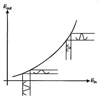
FIG 14 Effect of nonlinearity in amplifier transfer characteristics.
So, if a signal is being amplified by such a nonlinear stage, and this is true whatever the nonlinear shape of the transfer characteristic, any mechanism -- such as an additional signal voltage being handled at the same time by the same amplifying stage- which causes the operating point to move up and down along the amplifier Em/Eout transfer curve, will have the effect of 'modulating' (increasing or reducing the size of) the resultant signal voltage.
When the mechanism for moving the operating point up and down is the presence of a second simultaneous signal voltage, the result will be that both output signals will be modulated by each other -- a phenomenon which is called 'cross modulation'. This effect will occur in any stage which suffers from any degree of waveform distortion, which, in practice, means virtually every real -- as distinct from theoretical -- system, and is of particular importance in wide band amplifier stages. This is because such amplifier stages will have a higher thermal noise component --see equation (1), above -- and because there is a greater probability, especially in radio frequency preamplifier systems, that one or more relatively powerful signals will be included within the amplifier pass-band. So, in the presence of such inevitable nonlinearities in the amplifier characteristics, all signals will be cross modulated by wideband noise, a noise component which will remain as a feature of each signal and will be unaffected by subsequent bandwidth limitation (apart from considerations of sideband curtailment). Furthermore, all signals which are present at the same time will, to some extent, cross-modulate each other: an effect which cannot subsequently be removed by later improvements in selectivity.
Some measure of relief is afforded by the fact that the effects of nonlinearity in an input transfer curve are related to the size of the input signal, so that the smaller the signal, the more closely the transfer characteristic will approximate to the ideal straight line shape, and the less significant cross-modulation, of all kinds, will be. However, the fact remains that the wider the band width any stage is called upon to handle, the greater the scope there will be for various operational problems.
Good amplifier design will therefore seek to combine the following requirements: that the gain of the input stage shall be sufficient to ensure that the noise contributions from all later stages will be less than that due to the input stage; that, for the same reasons, the inter-stage couplings shall be chosen to achieve the best possible transfer of signal energy from each stage to the next; that the effective bandwidth of any stage is never greater than is necessary; that all stages have the maximum practicable linearity of their transfer characteristics; and that the signal level at any point in the system is never allowed to exceed that which can be accommodated within an adequately linear part of the transfer curve. It could also be added that it’s a useful design ambition to try to achieve the required performance with the minimum feasible number of stages: what isn't there won't add noise, and can't go wrong.
Wide bandwidth amplifier design
There are three main difficulties in obtaining a good high frequency performance from a simple transistor amplifier, of the kind shown in FIG15, ignoring for the moment such arcane things as carrier transit time effects within the device. These are the effect of the collector-base feedback capacitance (C^), the out put stray capacitance (Cs), and the input (base-emitter) capacitance (Cin), which is largely due to the forward biased base-emitter junction diode, an important factor which will be examined later.
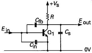
FIG15
The importance of the feedback capacitance, in a simple resistance-capacitance coupled amplifier, is mainly due to the fact that since the stage is a voltage inverting one, an input voltage of y will give rise to an output voltage of -Ay, where A is the amplification factor of the stage. This means that the input voltage y will cause a total voltage of -(A+1)j to develop across the capacitor, so that the input charging current required to allow a voltage change to arise at the input of the device will be A+1 times greater than if the output end of C_fb was just connected to the 0V rail.
This effective magnification of the size of the feed back capacitance is known as the 'Miller effect', and, for a feedback capacitance of 5pF and a stage gain of 50, this effect would make the capacitance seen at the input appear to be 255pF. If we define the Miller capacitance as Cm, then to get a useful degree of amplification, at, say, 5MHz from such a stage would demand that the source impedance (Zs) is significantly lower than that of Cm at 5MHz, i.e. less than 127 ohms.
The effect of the stray capacitance (Cs) from the output point to earth, depends on the charge/discharge time constant of Cs and R . Again, for a -3dB point in the gain curve at 5MHz, for a 10pF value of stray capacitance, the load resistor cannot exceed 3k. (Both of these resistor values are derived from the equation Zc=1/[27 pi C].
The simplest way of minimizing the effect of Miller capacitance is to use either a grounded base, or a differential amplifier or a cascode layout, of the kinds shown in FIGs 5, 8,9,and 10, modified for use in a resistance coupled layout as shown in the circuits given in FIG16.
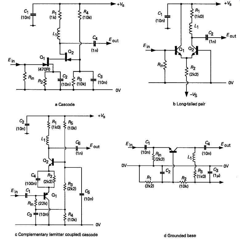
FIG 16 Practical wide bandwidth amplifier circuits.
a. Cascode; b. Long-tailed pair; c. Complementary (emitter coupled) cascode; d. Grounded base
A dual gate MOSFET could also be employed as the amplifier stage, but such a device, though excellent in respect of its very low feedback (Miller) capacitance, would have limitations in respect of its possible drain current, which might need to be fairly high in order to achieve a useful output voltage swing with a low value collector or drain load resistor.
A further common technique, illustrated in FIGs 16, is to incorporate a small inductor, Ll9 in series with RL. The value of this inductor will be chosen to resonate with the stray capacitance, as a parallel tuned circuit, at a frequency close to the upper -3dB gain point of the amplifier stage. This will give a boost to the gain of the stage at this frequency, and may allow higher values of load resistor to be employed -- which will give a higher stage gain -- for the same value of stray capacitance.
An alternative approach which is also used, where the amplifier stage is to be used to drive a known capacitative load, such as a long length of cable, is to include an inductor, L2, as shown in FIG17, in series with the output circuit, with the value of L2 chosen to resonate with Cs as a series tuned circuit, in order to generate a higher output voltage at the HF end of the specified pass-band.
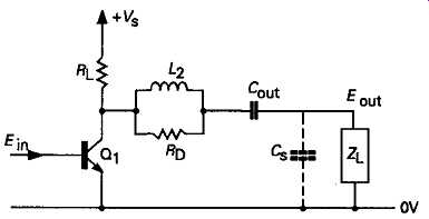
FIG 17 Series inductor output RF compensation.
Another very useful way of limiting the shunting effect of the load stray capacitances on the amplifier load resistor is simply to interpose an output emitter follower (or its FET equivalents) between the gain stage and the load circuit, as shown in FIG18.
This will allow an effective output impedance, as seen by the load, of less than 100 ohms, with a consequent substantial increase in the effective gain/bandwidth product of the stage. Some caution is needed, however, in the use of this kind of circuit, in that an emitter follower can break into oscillation, at VHF, with certain values of output load capacitance and inductance, due to its internal stray capacitances and carrier transit times. This type of mechanism is explained more fully in Section 13.
FIG 18 Output emitter follower impedance converter
For very high frequency use, the load resistor may be dispensed with entirely, as shown in FIG19, so that the load inductor, Ll9 acts simply as an RF choke -- a load whose RF impedance increases with frequency, but whose DC resistance can be quite low -- allowing relatively high values of collector current to flow, with consequently increased values of amplifier transfer conductance (gm), expressed as milliamperes of change in output current for a unit voltage change in the applied input potential. The drawback with this arrangement, apart from the fact that the stage gain will be very low at low frequencies, is the fact that above the frequency of resonance of the choke with the load stray capacitance, the output load will appear to be purely capacitative, and the stage gain will consequently fall linearly with increasing frequency.
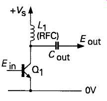
FIG 19 RF choke used as load
Although, for simplicity, I have illustrated the preceding amplifier stages as using a single transistor, designers will, in practice, more often choose to use a gain stage, such as the cascode layout shown in FIG20, which will limit the effects of Miller capacitance.
FIG 20 Cascode connected wide-band amplifier stage.
Effects of junction capacitances
The capacitances within a junction transistor are com posed of two separate components, the 'stray' capacitances which are simply due to the physical proximity of the connecting wires, and those which are due to the presence of the collector-base and base emitter junction diodes.
In normal operation, the collector-base junction is reverse biased, so this diode looks like any other junction capacitor of equivalent area and doping level, and will offer a capacitance (C:) which will vary with the reverse bias level in an identical manner to the well known 'Varicap' tuning diode, whose capacitance is given approximately by the equation ...
...where V is the applied voltage, m is a constant depending on the junction area, thickness and doping level, and Vd is the forward diode conduction voltage --approximately 0.6V for silicon devices.
Under normal small-signal operating conditions the collector-base voltage will remain substantially constant, so that C1 can be considered simply as an internal device capacitance in much the same way as the anode -- grid capacitance of a valve -- the treatment I have adopted above. Unfortunately, the effect of the for ward biased base-emitter junction is much more complex, because the effective capacitance for a given junction area will be much larger, and much more strongly dependent on doping level and bias voltage, especially the latter. For this reason, transistor manufacturers don’t attempt to specify the effective base emitter junction capacitance, but, instead, quote the value of the effective 'current gain transition frequency', or 'gain/bandwidth product', 'fT', which largely depends on it. This type of specification is, in any case, rather misleading in its apparent implication, since a quoted value 'fT = 400MHz' tends to give the impression that some useful gain might be available at this frequency, whereas, in reality, this is the frequency at which the current gain has fallen to unity in value, so, a transistor with an Af e (common emitter current gain) of 400 would have a-3dB point in its gain value at 1MHz,not 400MHz!
The transition frequency value for a bipolar junction transistor is a complex factor, and depends on the geometry of the device, including particularly the junction thickness, the doping level, the carrier mobility, as well as the effective input (base-emitter) capacitance, in that this will provide an alternative path to ground for the input signal current. The internal base-emitter conducting impedance (re), decreases as the emitter (and base) current increases. Unfortunately, the base-emitter junction capacitance (Cie) also increases, so that, for any given source impedance, the proportion of the input current which is usefully employed increases only slowly with an in crease in emitter/collector current, with most small signal transistors giving their best HF performance at collector currents in the range 5-100mA, where the effective base-emitter (input) capacitance of the transistor will be in the range 10-100pF.
There is little the designer can do to minimize the effect of this input capacitance on circuit performance except that since the gain/bandwidth product, an alter native name given t of T, remains fairly flat over a range of collector current values, whereas the base-emitter capacitance will increase over this range, as shown in FIG21, it’s sensible to operate bipolar junction transistor gain stages at the lowest collector current capable of giving an adequate value of f_T.
In the case of bipolar junction transistors specifically designed for use at high frequencies, efforts will have been made to keep the junction areas, and those stray capacitances of purely mechanical origin, as low as possible, and also to keep the junction regions as thin as feasible for a given maximum collector voltage, in order to keep the carrier transit times low. Because of the low circuit impedance levels usable with bipolar junction transistors, and the very high mutual conductance values which they offer, these devices are still preferable for low noise, high gain and wide band width amplifier stages, in spite of the practical difficulties in circuit design.

FIG 21 Effect of collector current on f_t and input capacitance in small
signal transistors. Gain bandwidth product; Collector current (mA)
Input bandwidth limitation
Since the problems of input noise level and possible cross-modulation effects are bandwidth related --hence the old adage that 'the wider the window, the more the dirt flies in'- it’s a sensible policy in amplifier design to limit the bandwidth to a value which does not greatly exceed that which is necessary for the purpose in hand.
Where amplification down to LF is not required, as, for example, in the case of a radio or TV receiver RF preamplifier stage, but where it’s not wished to select the particular frequency to be amplified at the input to the amplifier- as might be the case in a radio receiver where the actual operating frequency is only decided at the frequency changer stage, later in the circuit -- an approach which is widely used is to use an input filter circuit which combines high-pass and low-pass characteristics. In principle, this might just consist of an LC low-pass and a CL high-pass pair of filter circuits in cascade, as shown in FIG22, but the performance of such a simple arrangement is unlikely to be adequate.
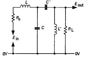
FIG 22. Layout of simple band-pass LC/CL filter.
However, design tables for high performance multiple element low-pass, high-pass and bandpass filters with a flat-topped pass-band frequency response, coupled with steep cut-off bandwidth skirts, are commonly given in RF circuit design textbooks (such as the ARRL Handbook, 1989. pp. 2.37-2.55), and a worked example, using diode switching, and covering the frequency range 3MHz-30MHz in three bands, is shown in FIG23.
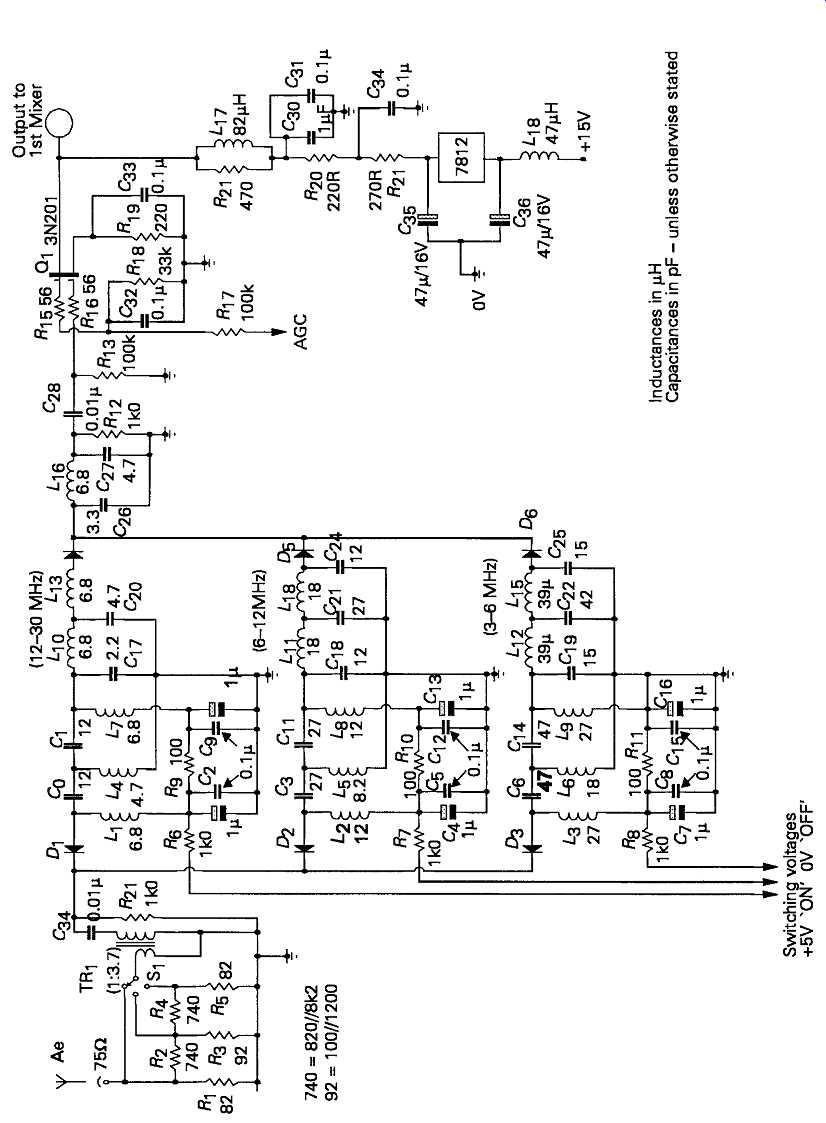
FIG 23 Typical input band-pass filter for 3-30MHz communications receiver
[Inductances in µF Capacitances in pF -- unless otherwise stated ]