AMAZON multi-meters discounts AMAZON oscilloscope discounts
Introduction
The requirements of simple industrial control mechanisms, and the exploration of non-mechanical digital computer systems would, undoubtedly, have led in due course to the utilization of the electronic emission phenomena uncovered by Edison, even if they had not been used by Fleming and Lee de Forrest, in the subsequent evolution of the thermionic valve. How ever, as a matter of history, the actual stimulus to the development of 'thermionics', and, following this, the exploration of electronics, as a whole, came from the commercial success of wireless telegraphy, by which means interrupted trains of high frequency alternating electric signals could be sent from a 'transmitter' to a 'receiver', without the need for a wired electrical connection between them.
In the early experiments in this field, the use of a high voltage 'spark generator', of the kind shown in FIG. 1, to shock excite a damped train of electrical oscillations in a tuned circuit, as indicated in FIG. 2, was quite adequate as a source of RF signals.
Such a transmitter, apart from its inefficiency and noisy output signal, would inevitably generate quite a wide spectrum of RF radiation, and it would be impracticable to operate two such transmitters in the same area, because of mutual interference, or to operate a transmitter, and a receiver, simultaneously at the same location, unless their operating frequencies were very widely separated.
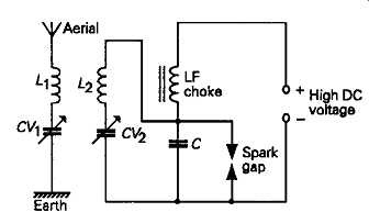
FIG. 1 Typical spark generator for RF [h High, DC voltage, Earth]
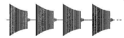
FIG. 2 Damped train of RF oscillations produced by circuit of FIG. 1
What was required was some way of generating a continuous single frequency sinewave voltage output, stable in both amplitude and frequency, and free from spurious harmonics or other unwanted signals, which could then be amplified and broadcast by the transmitter aerial. This is not an easy requirement to meet, and an enormous amount of ingenuity has been directed, over the years, to devising circuitry for this purpose.
Undoubtedly, the starting point for this development was the invention of feedback, by E. H. Armstrong, in 1912: a technique in which an amplified signal was fed back into the input circuit of the amplifier, which provided an effective means of generating such a continuous oscillation. Sadly, Armstrong discovered, like many other inventors before and since, that making a useful invention and defending the title and ownership of it through subsequent, and normally unavoidable, litigation, were two very different things, and the rest of his life was plagued by the continuing need to preserve his rights in the use of the many useful ideas he had originated. However, I am happy, on behalf of my fellow electronics engineers, to acknowledge the debt we owe to him.
Although, in the beginning, oscillator circuits were mainly required as the signal source for transmitters --a need which still remains -- increasingly, with the passage of time, other applications are being found, such as the use of oscillators in receiver circuitry for frequency conversion purposes, as tone generators in electronic music, as frequency standards, test signal sources and waveform generators in a whole host of applications, and as frequency control clock mechanisms for a whole range of digital circuitry.
For convenience, I have divided this section into three parts, covering those types of oscillator based on tuned LC circuits, those utilizing electromechanical effects in piezo-electric materials ('crystal' oscillators), and those based on RC relaxation effects -- as an extension of the various multivibrator designs examined in Section 10.
Basic circuit designs frequency HF oscillator designs, and are based on the use of the LC tuned circuit arrangement examined in Section 11. In all of these designs a tuned circuit is used to select the actual frequency of oscillation, and the layout of an electronic circuit containing an amplifier is arranged to provide the positive voltage or current feedback needed to sustain oscillation.
Although there are literally scores of different LC oscillator circuits which have been developed for various applications, there appear to be seven basic forms, from which individual circuits have been derived. Since all of these circuits were devised at a period when the only amplifying element available to the designer was the electronic valve, which acts as a high input impedance phase inverting gain stage, I have illustrated these basic oscillator designs, in schematic form, in FIGs 3 to 10, using a simple high input impedance phase inverting gain block, A1 A2, etc., to simulate the function of the valve.
For some of the circuits, the operation of the circuit, in an elaborated form, depends on the physical characteristics of the amplifying device, as in the electron coupled oscillator, and in this case I will show either the valve circuit or one based on a contemporary solid-state equivalent device, such as a junction FET.
Hartley:
In this layout, shown in FIG. 3, the inductor (Lx) in the LC tuned circuit has an intermediary connection, a 'tap', usually but not necessarily somewhere near its centre point, which is taken to a zero RF potential point. This causes the instantaneous RF potential at the two ends of the coil to be in antiphase, which gives the phase inversion in the feedback path needed to meet the requirement for oscillation.
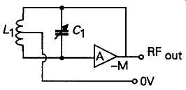
FIG. 3 Hartley oscillator -- LC oscillators
Colpitts:
Because of the general purity of their output wave form, these systems form the majority of the variable This arrangement, shown in FIG. 4, is very similar in its function to the Hartley circuit of FIG. 3, except that, in this case, the tuning capacitor in the LC circuit is divided into two (C1 and C2), and the junction of these is taken to a low impedance point. As a matter of practical convenience, C1 will often have the same value as C2, but this does not need to be the case, and in some applications better performance might be obtained by the use of a different C1/C2 ratio.
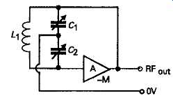
FIG. 4 Colpitts oscillator
Tuned input:
In this layout, shown in FIG. 5, the tuned circuit is elaborated into a two-winding HF transformer, of which the tuned secondary is connected to the input of the gain block, and the primary feedback winding, taken from the amplifier output, is connected in such a way that the necessary positive feedback is obtained.
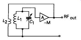
FIG. 5 Tuned input oscillator
Tuned output:
This circuit, shown in FIG. 6, is basically identical in its design philosophy to that of the tuned input layout, except that, in this case, it’s the primary winding of the output-input coupling transformer which is tuned. This has the advantage, where high voltage outputs are needed, that the transformation ratio can be chosen so that a large voltage swing can be developed at the output without overloading the input circuit.
Meissner:
This oscillator, shown in FIG. 7, employs a tuned FIG. 6 Tuned output oscillator circuit in which the frequency of resonance is deter mined by the presence of a third resonant winding, tightly coupled, inductively, to the transformer primary and secondary circuits. Apart from the greater ease of developing a large output voltage swing across the tuned winding, this circuit offers few advantages to offset its additional complexity, and is seldom used in contemporary designs.
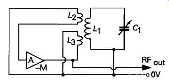
FIG. 7 The Meissner circuit
Capacitive feedback:
In this layout, shown in FIG. 8a, oscillation will occur, due to the combination of capacitative voltage feedback through C^ and the phase shift in the input and output circuits which occurs near resonance, when the input and output tuned circuits are tuned to very nearly the same frequency. This phenomenon was discussed in Section 12, in relation to the problems encountered with early tuned RF amplifier designs, which were invariably unstable in operation due to this phenomenon.
Such circuit layouts, based on triode valves, as shown in FIG. 8b, are usually described as 'tuned anode, tuned grid' (TATG) oscillators, and are still quite commonly found in simple radio transmitter circuitry, mainly because they allow such a high RF output voltages to be developed at the valve anode.
With a 300V +ve supply line, and a suitable anode coil/capacitor combination, RF voltages of 10kV RMS, or more can be generated -- probably mainly limited by internal arcing within the valve or across the tuning capacitor!
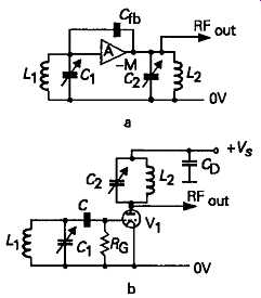
FIG. 8 -- Capacitive feedback (TATG) oscillators
Negative impedance oscillators
In these circuits, of which one form is illustrated schematically in FIG. 9, the tuned circuit is used to determine the frequency of oscillation, and an external gain block combination, such as the amplifier chain in the diagram, is used to generate an externally applied negative impedance characteristic. If this negative impedance is greater than, or equal to, the resistive circuit losses present in the tuned circuit, oscillation will occur at the LC resonant frequency.
With a pair of valve amplifiers employed as the gain blocks, this circuit is called the ' Franklin' oscillator, and was noted for its very high stability in operating frequency, because it would operate with very 'loose' coupling (very small values of capacitors) between the tuned circuit and the external amplifier chain.
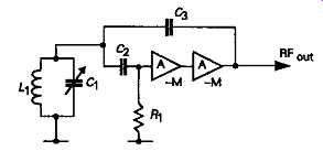
FIG. 9 Franklin type of negative impedance oscillator
A modem circuit, using basically the same method of generating oscillation, is the tunnel diode circuit shown in FIG. 10, in which the diode offers a negative resistance characteristic over part of its for ward bias current range, a mechanism which was explained in Section 4.
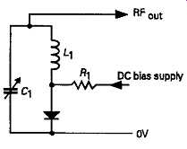
FIG. 10 Tunnel diode oscillator
Practical oscillator systems:
The major requirements for any oscillator are that it should be stable in frequency and output amplitude, and that it should have an output waveform which is adequately free of noise, harmonics or overtones, and spurious parasitic signals. This latter requirement is not as easy to meet as the designer would wish, and, for a high degree of purity in the output frequency spectrum, demands great care in the physical layout of the oscillator circuit, to avoid unexpected inductance/capacitance loops.
Frequency stability in a system based on an LC tuned circuit normally requires that the operating temperature of the whole system shall be held constant, and that the external amplifier or output load circuit shall not have a significant influence on the resonant frequency of the tuned circuit. It’s also necessary that the inductor -- usually just called a 'coil' in normal radio parlance -- and the capacitor shall be stable in value, in respect of physical shocks and vibration, which usually means that they must be physically robust, and well screened from outside inductive and capacitative effects.
One way of minimizing the effect which an external load might have upon the operating frequency of the tuned circuit is to take advantage of the fact that in a screened grid or RF pentode type of valve, the screening grid can also act as a triode anode, and this allows the rearrangement of a Hartley oscillator circuit, as shown in FIG. 11, in which this effective anode is earthed, and the output of the amplifier circuit is coupled to the tuned circuit by means of a tap on L1, connected to the valve cathode. In this arrangement, the voltage gain needed to bring about oscillation is obtained from the step-up transformer action of the tap on Lj, driven from the low impedance cathode circuit.
The electron flow through the valve to the anode is then used to couple the oscillator section of the valve to the output, which minimizes the influence which the external load may have, and thereby improves the frequency stability of the oscillator.
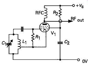
FIG. 11 Circuit of electron-coupled or cathode-coupled Hartley oscillator.
Because of its action, this circuit layout is called an 'electron coupled oscillator' or ECO. It’s also known as a cathode-coupled Hartley oscillator.
To prevent waveform distortion due to clipping, it’s necessary to provide some mechanism by which the output waveform amplitude can be limited automatically at some point below the clipping level. This can be done quite effectively in valve operated circuits, as shown in FIG. 11, by the mechanism called 'self biasing'. This uses the input capacitor-resistor combi nation, C2/R1, to store a negative charge on C2, each time the grid of the valve is driven positively beyond the point at which grid conduction occurs. This results in an average level of negative DC bias being developed at the grid of the valve which is proportional to the peak AC voltage present at this point, and biases the valve back to a lower gain part of its operating characteristics, which stabilizes the output voltage at some point below the clipping level.
The 'peak clipping' effect of grid conduction causes some degree of high order harmonic distortion in the output waveform -- a problem which is minimized by the use of a high Q tuned circuit. A further snag with this arrangement is that the values of C2 and R1 must be chosen with care, in that if they are too large, in relation to the operating frequency, the problem known as 'squegging' -- a continuous sawtooth shaped modulation of the output amplitude -- can occur. If squegging occurs at a high enough frequency, it may not be recognized for what it is, and simply seem to be an unduly high oscillator noise level. Squegging is employed beneficially in super-regenerative receivers (another invention due to Armstrong), discussed in Section 14.
A version of the circuit of FIG. 11, using a junction FET cascode layout is shown in FIG. 12.
Since the gate junction of the FET is a simple junction diode, self-biasing can also be employed, though it does not work as well as with thermionic valves, and a thermistor, of the type having a very low thermal mass, and designed for oscillator amplitude stabilization, connected in parallel across part of L1 may be a better control mechanism.
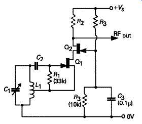
FIG. 12 FET cascode
ECO arrangement
The Colpitts circuit may also be used in a cathode coupled (or source- or emitter-coupled) electron coupled layout, as shown in FIG. 13. In this case, because there is no DC return path through Lx for the cathode current, an RF choke (RFC2) is used to complete the DC circuit. A simpler circuit of the same type, though, in this case, with the RF output taken from the source electrode, is shown in a FET version in FIG. 14.
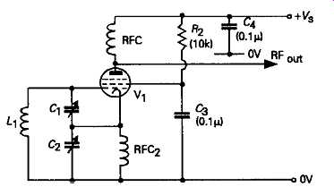
FIG. 13 Cathode-coupled Colpitts oscillator using PNP transistor
The connection of the main LC resonant circuit in a series, rather than a parallel form, has attracted interest as a technique offering improved frequency stability, because of the lower impedance offered to the external
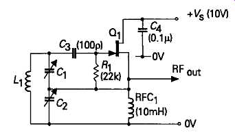
FIG. 14 FET source-coupled oscillator gain block. The best known of these
layouts, using a Colpitts type feedback connection, is the 'Clapp-Gouriet'
design, shown in FIG. 15. As a matter of historical curiosity, the reason
for the double-barreled name is that the layout was invented separately and
independently by two engineers, G. C. Gouriet and J. K. Clapp, in 1947-8.
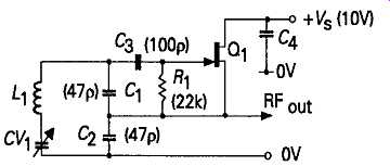
FIG. 15 Transistor operated Clapp-Gouriet type of oscillator
Another layout with a similar configuration, and which also enjoys a high reputation for frequency stability, among amateur radio enthusiasts, is the 'Vackar' circuit, shown in FIG. 16, although, in this case, the source of the FET is earthed, so the RF output must be taken from the drain circuit.
I have already emphasized that nearly all of the circuits shown can be built equally well using valves, bipolar transistors, junction FETs or MOSFETs, pro vided that the layout is arranged to give the correct DC working conditions, and that suitable means are employed to control the amplitude of oscillation. How ever, in some cases, the availability of complementary polarity semiconductor devices (i.e. PNP as well as NPN) leads to particularly convenient transistor circuit layouts, such as the modified Colpitts arrangement shown in FIG. 17. This layout offers good frequency stability, and will operate at frequencies well above 100MHz.
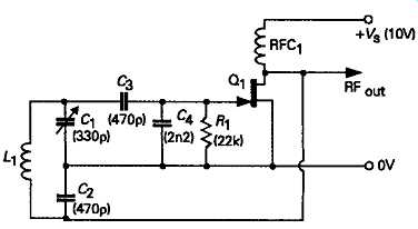
FIG. 16 The Vackar oscillator
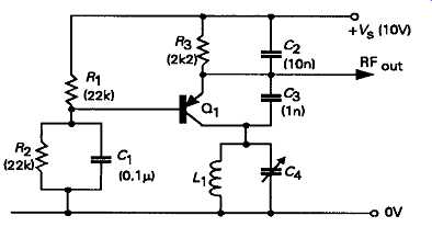
FIG. 17 Modified Colpitts oscillator using- PNP transistor
A variation of the Franklin circuit- a layout in which the external amplifier consists of two phase inverting stages connected in cascade, so that the tuned circuit does not need to provide the in-phase feedback signal -- is the source-coupled design shown in FIG. 18.
This arrangement works well with valves, FETs and MOSFETs, but is less suited to use with bipolar transistors.
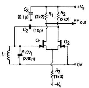
FIG. 18 Source-coupled Franklin oscillator.
An interesting development of this circuit is the Butler layout, where the inter-stage signal path is completed by way of a series resonant tuned circuit connected between the sources (or cathodes) of the amplifying devices, as in the FET arrangement shown in FIG. 19. This layout shares with the Clapp Gouriet and Vackar circuits the desirable characteristic that the RF output voltage of the oscillator remains substantially constant over the tuning range, whereas most of the systems using parallel resonant LC circuits as their frequency determining components tend to show an output voltage which decreases as the value of the tuning capacitor, CVV is increased, because this reduces both the dynamic impedance (L/Cr) and the Q (1/r V(X/Q) of the tuned circuit.
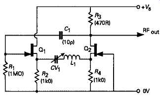
FIG. 19 FET operated Butler oscillator
The use of a series resonant circuit in a modified Colpitts configuration, of the kind shown schematically in FIG. 20 -- which can be thought of as either an LC version of the Pierce crystal oscillator ( FIG. 23), or yet a further rearrangement of the Clapp layout -- allows the tuned circuit to be isolated from the relatively low input impedance of the bipolar junction transistor, which allows improved frequency stability and increased output voltage swing. This layout was employed in a symmetrical push-pull version, in a circuit of my own, shown in FIG. 21, which was used as a high output voltage HF bias oscillator in a tape recorder design (Wireless World, February 1978, p. 36).
Quartz crystal oscillators
Fundamental frequency types:
The use of the electro-mechanical piezo-electric effect in quartz crystals, to provide a very high Q equivalent to a tuned circuit, was examined in Section 12. Where a very high degree of precision and stability in the operating frequency of an oscillator circuit is needed, the quartz crystal (or its near equivalent, the quartz surface acoustic wave resonator) is by far the best low cost option, though it imposes a need for operation at, or very close to, a fixed 'spot' frequency, determined by the physical dimensions of the crystal, and this limitation may be inconvenient.
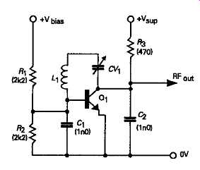
FIG. 20 Modified Colpitts oscillator
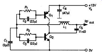
FIG. 21 Modified Colpitts oscillator used as tape recorder HF bias source.
As can be seen from its equivalent electrical circuit, shown in FIG. 22, its principal mode of operation is that of a series resonant circuit -- though it can operate as a parallel resonant circuit because of the inevitable holder, mount, and other stray capacitances (C0). This means that quartz crystal oscillator systems will operate most happily in those kinds of circuit --such as the Clapp, or Butler or Pierce designs, shown in FIG. 23 -- which have been developed for use with series resonant LC layouts.
In the Pierce crystal oscillator design the capacitor, C1? in series with the crystal is mainly used to ensure that the crystal has the recommended load capacitance for its specified frequency of operation.
A selection of typical circuit arrangements is shown in FIG. s 23-33, of which the first is the layout usually called the Miller or Pierce-Miller design, which is very similar in its method of operation to the tuned anode, tuned grid (TATG) design shown in FIG. 8b. A rather more conventional Colpitts type layout, shown in FIG. 25, is widely recommended for use over the frequency range 100kHz-20MHz.
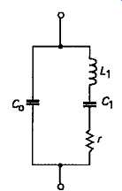
FIG. 22 Equivalent circuit of quartz crystal resonator.
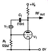
FIG. 23 Pierce oscillator.
A type of Pierce oscillator which is well suited for use with CMOS-type inverting buffers, is the layout shown in FIG. 26. A somewhat less satisfactory arrangement, which is, nevertheless very widely used, is the circuit shown in FIG. 27. This has the intrinsic drawback that the circuit has overall positive feedback, and could therefore still oscillate if the crystal were to be replaced by a small capacitor. This means that there is no real guarantee that the frequency of oscillation is that due to crystal resonance, although it’s probable that it will be.
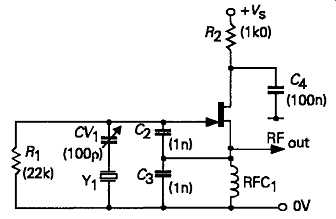
FIG. 25 Colpitts crystal oscillator circuit
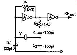
FIG. 26 CMOS quartz crystal oscillator
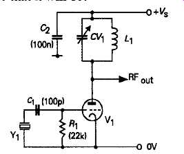
FIG. 24 Fierce-Miller crystal oscillator
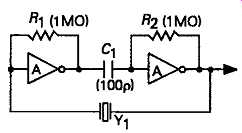
FIG. 27 Logic gate crystal oscillator
Overtone oscillators:
Increasing the operating frequency of a quartz crystal resonator operating in its fundamental resonant mode entails increasing thinness, and fragility, in the crystal slice. It’s therefore customary for crystal oscillators operating at higher frequencies to utilize overtone modes of oscillation, based on the 3rd or 5th harmonics of the fundamental resonant frequency -- a mechanism considered in Section 11.
The simplest version of this kind of layout is that shown in FIG. 24, which is a TATG or capacitive feedback (Miller) type of oscillator, in which the anode LC circuit (L1CV1) is tuned to the required crystal harmonic, though satisfactory operation may require a crystal designed for this application. The input resistor, R1 is used to provide self biasing for amplitude stabilization.
With all crystal oscillator designs, and particularly so with TATG derivatives, care must be taken to pre vent the crystal applied RF voltage and power dissipations from being exceeded, in that this may damage the crystal, as well as impairing its frequency stability.
Two similar circuits designed specifically for use with crystals made for overtone operation, up to some 105MHz, are shown in FIG. 28 and 29. These are Colpitts oscillators, in which an external series resonant circuit, comprising Lx and the stray capacitances of the crystal and holder, is used to force oscillation at the required harmonic frequency. The values of Rx and C2/C3 will depend on the operating frequency range, with lower values required at higher frequencies. Like the inverting logic IC layout of FIG. 27, these circuits suffer from the drawback that they can oscillate at a frequency not specifically determined by the crystal.
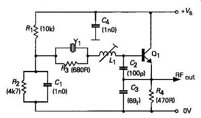
FIG. 28 Crystal overtone oscillator based on Colpitts system.
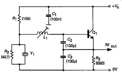
FIG. 29 Colpitts-based crystal overtone oscillator.
An alternative approach to the harmonic operation of a crystal, which does not rely on the use of a crystal specifically designed for this application, is just to select the required harmonic output from a crystal oscillating in its fundamental mode, as with the Colpitts layout shown in FIG. 30, where the output circuit is tuned to the required harmonic frequency.
The same approach can be used with the Butler oscillator of FIG. 31. Two other useful overtone oscillators arc the Robert Dollar design of FIG. 32, and the grounded base circuit of FIG. 33.
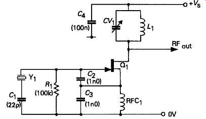
FIG. 30 Crystal controlled overtone oscillator
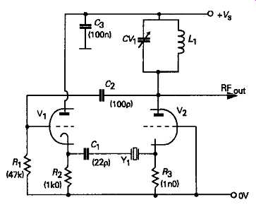
FIG. 31 Butler overtone oscillator
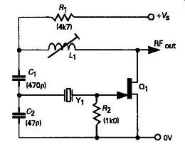
FIG. 32 The Robert Dollar overtone oscillator
As mentioned in Section 11 there are also surface acoustic wave resonators, which offer frequency stability values which approach those of quartz crystals, but which can operate in their fundamental mode at frequencies up to 500MHz.
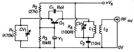
FIG. 33 Grounded-base 3rdl5th harmonic crystal oscillator circuit.
VXOs:
Frequency trimmed quartz crystal oscillators, known as VXOs (to distinguish them from standard frequency crystal oscillators, known in radio jargon as XOs), are basically standard XO designs in which a small shift in operating frequency is brought about by a manually adjustable trimmer capacitor, usually in the range 20-100pF, connected in series or parallel with the crystal, as shown, for example, in FIG. 25.
RC oscillators:
In principle, any normal RC multivibrator, of the type shown in FIG. 34, can also operate as an HF oscillator, up to a maximum frequency determined by the characteristics of the transistor and the shunting effect of stray capacitances, bearing in mind that the values of C1 and C2 will also need to be smaller for the shorter charge/discharge times needed for higher frequency operation. If the transistors are driven into current saturation, there will be a finite recovery time in their conduction characteristics, because of the time required for depletion layer minority carriers to be swept up by the applied field: a time which will decrease with increasing supply voltages. FETs and MOSFETs are free from this particular defect.
Although thermionic valves are also free from the carrier recombination type problems of junction semi conductors, multi-vibrators based on these are limited in maximum operating frequency by stray capacitances and inter-electrode electron transit times, as well as the inevitably large unwanted circuit inductances due to their connecting leads. This means, in practice, that their maximum operating frequencies are usually much lower than possible with solid-state designs.
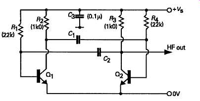
FIG. 34 Simple multivibrator circuit usable up to perhaps 200kHz
Circuit designs such as the long-tailed pair layout of FIG. 35 offer much higher possible operating frequencies, up to, say, 15MHz, because the transistors are not driven into current saturation. The basic Bowes type emitter-coupled astable multivibrator, shown in FIG. 36, is also capable of operation at frequencies up to 10MHz.
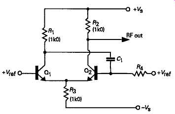
FIG. 35 Emitter-coupled multivibrator having better HF performance
Problems with RC oscillators:
There are a number of difficulties in the use of astable RC oscillators (multi-vibrators) at high frequencies, as RF signal sources. To begin with, such oscillators offer relatively poor stability in operating frequency, due to the fact that a whole range of different effects, such as transistor junction temperature, supply voltage and junction turn-on voltage, affect the duration of any on or off cycle. It also requires care to prevent the operating frequency being affected by the output load impedance.
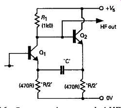
FIG. 36 Bowes emitter-coupled HF multivibrator.
A more subtle problem in the operation of all RC relaxation-type oscillators, is that there is always a degree of statistical randomness in the actual point in time at which a transistor turns on or off , in such a circuit, due mainly to the effect of thermal voltage noise on junction potential. This leads to a relatively large frequency modulated, and a somewhat smaller amplitude modulated, noise component in the output signal. This would mean that if the output of the oscillator were combined with some other signal, as, for example, as the local oscillator in a superhet radio frequency changer stage, or added to the recorded signal, as the bias oscillator in a magnetic tape recorder, the final signal to noise ratio of the system will be worsened -- especially if the amplitude of the RC oscillator voltage, and therefore its noise component, is large in comparison with the signal voltage to which it’s added.
Voltage controlled oscillators (VCOs):
This category embraces a wide range of oscillator circuit designs, in which the operating frequency will depend on some applied voltage. With RC oscillator types, two general approaches are used, to alter the reference voltage to which the base of Q2 is taken, in the circuit of FIG. 35, which alters the voltage to which the base of Q2 must climb or descend, through C1 R1 and R3, before Q1 and Q2 turn on or off, which will alter the operating frequency.
The other approach is to directly control the charging or discharging current of the timing capacitor, as, for example, C1 in FIG. 37, through CC^ If the resistance of CC^ is lowered, the operating frequency of the oscillator is increased, and conversely. This is the technique which is used, in one form or another, in most of the integrated circuit VCOs, though it’s often difficult to achieve a reasonably linear relationship between applied voltage and operating frequency. A design of my own (Wireless World, November, 1973, pp. 367-369), which gives a highly linear relationship between applied voltage and operating frequency, is shown in FIG. 38. This circuit was used as the VCO in a phase-locked loop FM demodulator, and, with the component values shown, was designed to cover the frequency range 9-14MHz. To assist in reducing circuit stray capacitances, which helps to achieve a high working frequency range, transistors Q1-Q5 are ? ^ °f CA3046 monolithic transistor array. In this circuit, Q1 and Q2 are connected as a current mirror (see Section 6), with the current flow through Q2 controlling the charge and discharge times of C1, and, in consequence, the operating frequency of the oscillator. Increasing the value of C1 would allow operation at lower frequencies.
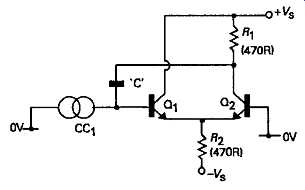
FIG. 37 Voltage controlled oscillator
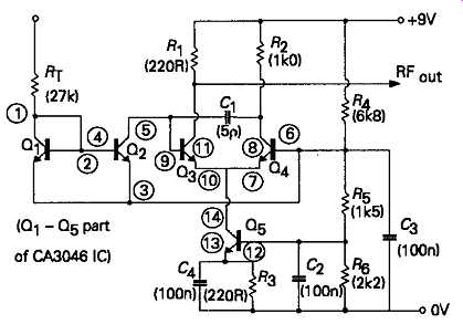
FIG. 38 Linear voltage controlled oscillator based on CA3046 transistor array
(pin numbers shown in brackets)
For most high frequency applications, the approach most commonly employed is just to connect a varicap diode (D^ -- a device which exploits the increase in the thickness of the depletion layer, and hence the decrease in capacitance, in a reverse biased P-N junction, as the applied voltage is increased -- in parallel with a standard parallel resonant tuned circuit (LJC2), as shown in FIG. 39, and then to use a change in the bias voltage applied to the diode to alter the resonant frequency of the tuned circuit. There are, however, two problems with this type of frequency control, of which the first is that there is a nonlinear relationship between the applied voltage and diode junction capacitance, of the general form C = kH(V + Vd), where m is a constant determined by the construction of the device, V is the applied voltage and Vd is approximately 0.6V for a silicon diode, as shown in Section 12 -- a relationship which results in a similar nonlinearity between control voltage and tuned circuit resonant frequency.
The second problem is that the relationship between capacitance and applied voltage is temperature de pendent. For some phase-locked loop frequency control systems, of the kind shown in FIG. 40, the operation of the internal feedback loop will maintain the chosen oscillator frequency so that neither the nonlinearity nor the poor frequency stability of the varicap control system are particularly important.
However, where varicap diode frequency control is used as the tuning mechanism for a radio receiver, the applied control voltage must be temperature compensated in order to minimize the extent of tuning drift.
Nevertheless, the great convenience of being able to tune a number of circuits simultaneously, by means of a remotely controlled voltage, has led to the very widespread adoption of this technique in radio receiver circuitry, with suitably temperature compensated control voltages.
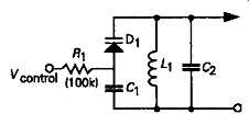
FIG. 39 Standard Varicap VCO arrangement
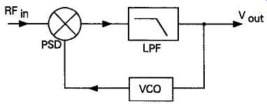
FIG. 40 Basic phase-locked loop system
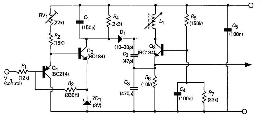
FIG. 41 Linear voltage controlled oscillator based on a varicap diode
A varicap tuned oscillator which is internally corrected both for temperature effects and nonlinearity, also used in an FM tuner phase-locked loop demodulator system (JLH, Wireless World, September 1979, pp. 87-88), is shown in FIG. 41. In this circuit, advantage is taken of the fact that the temperature dependence of characteristics, and the nonlinear relationship between base voltage and collector current in a bipolar transistor (in this case Q2), is of the same form, but opposite in curvature, to that of the varicap diode D1. This condition requires that Q2 should be driven from a low impedance source (in this case Q1, acting as an emitter follower), and the base-emitter DC offset of Q2, which will also be temperature dependent, is cancelled by the opposed connection of Q1 and Q2 The resulting linearized voltage vs. oscillator frequency characteristics arc shown in FIG. 42.
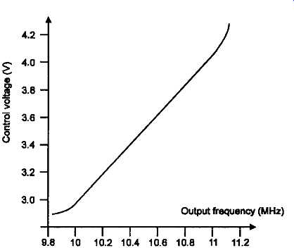
FIG. 42 Frequency response of circuit of FIG. 41. Output frequency (MHz)