AMAZON multi-meters discounts AMAZON oscilloscope discounts
...cont. from part 1
Shunt regulator layouts:
The simplest example of this type of system is the zener or avalanche diode circuit shown in FIG. 15. (Note. Although true zener diodes are only those with a turn-over voltage of about 5V or below, the term zener has come to be used as a generic term for all reverse breakdown regulator devices.) Such a layout is called a shunt regulator because the voltage sensitive component/s are connected so that they will draw current in parallel with the load, and will increase their current flow if the load current is reduced or the output voltage tends to increase.
In the circuit of FIG. 15, the input supply voltage, V, the value of the series resistance, R19 and the power handling capacity of the zener diode, D1, are chosen so that the required output voltage will be provided, without exceeding the permitted dissipation of the diode, at zero output current demand, but so there will always be an adequate current flow through the diode at the maximum likely load current. The output source resistance is determined by the slope of the diode voltage, Vd, when plotted against diode current, 7d, as shown in FIG. 16. For example, if the diode characteristics are such that an increase in current of 100mA causes an increase in the voltage developed across the diode of 0.1V, the effective source resistance will be one ohm, the attenuation of the input voltage ripple, for the circuit values quoted in FIG. 15, will be 50:1, and the required dissipation for D1 will be 0.6W. Unfortunately, for reasons examined in Section 4, both zener and avalanche diodes generate a small amount of wideband noise, so it’s probably worthwhile to connect a capacitor, C1, in parallel with the diode output to reduce somewhat this noise contribution.
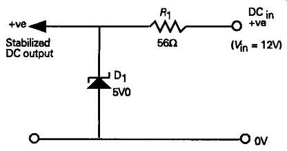
FIG. 15 Simple zener diode shunt regulator system
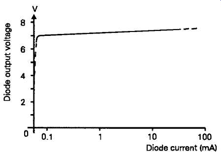
FIG. 16 Typical zener diode regulation characteristics
For low voltages a simple forward biased silicon junction diode is usable as a reference source, and will give an output voltage between 0.55V and 0.65V, depending on diode current, with a very low electrical noise contribution. Several such diodes could be connected in series, as shown in FIG. 17, to give, for example, a 2.4V DC source.
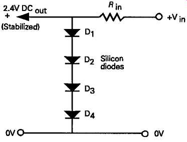
FIG. 17 Forward biased diode chain
The output characteristics of the simple zener diode circuit of FIG. 15 can be substantially improved by connecting the diode in the base circuit of an amplifying transistor, as shown in FIG. 18. This also allows a low-power diode to be used, which is useful since medium to high power transistors are usually cheaper than zener diodes having the same dissipation ratings. Also, since voltage regulator diodes, with turn-over voltages above some 5 V, have a positive temperature coefficient of output voltage-depending somewhat on diode current for a given junction area, as shown in Fig 19, -- while normal silicon junction diodes, such as the base-emitter junction of a transistor, have a negative temperature coefficient, connecting these in series, as in FIG. 18, can partially compensate for the positive temperature coefficient of the diode.
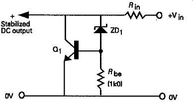
FIG. 18 Improved zener diode shunt regulator
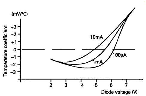
FIG. 19 Temperature coefficient of zener diode regulator.
Another simple shunt regulator layout is the so called 'amplified diode' circuit shown in FIG. 20. In this the transistor conducts if the voltage developed across R3 exceeds some 0.55-0.6V, giving an output voltage of Vbe (R2+^3)^3, which is adjustable, within limits, by the choice of values of R2 or R3. This type of layout is commonly used as a method of stabilizing the forward bias on the output transistor pair in class AB audio amplifiers, where Q1 will often be mounted in thermal contact with the output transistor heat sink, in order to provide a measure of operating temperature compensation.
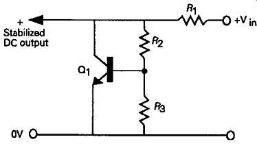
FIG. 20 The amplified diode circuit
More elaborate shunt regulator systems, of the type shown schematically in FIG. 21 -- in which the output voltage is compared with a precision voltage reference source, and the difference voltage is amplified and used to control a shunt transistor load -- can be used to provide improved regulation characteristics, but this layout is only likely to be used where the difference between the available input supply volt age and the required output voltage is so small that a series regulator circuit would be impracticable.
Series voltage regulator systems:
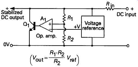
FIG. 21 High stability shunt voltage regulator circuit.
This type of circuit layout is one in which a series transistor, or equivalent device, is interposed between the input voltage source and the output point, so that, if the output voltage tends to rise above, or fall below the target figure, then the current flow through the series (pass) transistor can be adjusted by some external circuit so that the required output voltage level is maintained.
The simplest feasible circuit for this purpose is one in which the base of the pass transistor is fed from a fixed voltage source, such as from a simple zener diode voltage regulator, as shown in FIG. 22. If the output voltage falls, the base-emitter voltage applied to Ch will increase, and so will the current through Qj. If the output voltage tends to increase, then both the forward bias on Q1, and the current flow through Q1 will decrease.
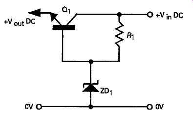
FIG. 22 stabilizer
Simple zener regulated series:
There are three main snags with this circuit, of which the first is that R1 must be able to pass a sufficient current to meet the base current demand of Q1 at the required maximum output current demand, plus what ever minimum current is required to cause the zener diode to operate. Secondly, the value of Rx cannot be made too low, or otherwise the desired attenuation of the input noise and ripple will be greatly lessened, and This means that the input voltage must exceed the required output voltage by an adequate amount.
Thirdly, the voltage across the zener diode will drop as more current is withdrawn by the base of the pass transistor, and the base-emitter voltage drop of Q1 as the output current demand is increased, will also become larger. Both of these effects operate in the same sense to reduce the output voltage provided by the circuit, and this gives the circuit a relatively high output (source) impedance.
A more conventional series regulator circuit will normally use the circuit layout shown in FIG. 23, in which the base current of the pass transistor is derived from the output of a voltage amplifier, whose input circuit is connected so that it’s able to sense the difference between its input voltage, -- usually related to the regulator output voltage -- and some stable and noise-free voltage reference source. If the output volt age from the regulator should vary, the amplifier will operate to oppose this variation. By the use of an error amplifier having sufficient gain a high degree of out put voltage stabilization, and a very low output impedance, typically less than 0.02 ohms, at frequencies up to a few kHz, can be obtained.
FIG. 23 Schematic layout of conventional series stabilization circuit.
The major drawback with this type of layout, in which the pass transistor is connected as an emitter follower, is that enough voltage difference must exist between the available input potential and the required output voltage for the amplifier to be able to drive the pass transistor adequately. The minimum input-output voltage requirement is commonly termed the 'drop out' voltage, and, with a well designed circuit can be as low as 2-3V.
The problem of the need to allow enough voltage drop in the circuit to provide forward bias for the transistor can be lessened by using the transistor in an inverted mode, in which the output current is drawn from its collector, so that the forward operating bias is derived from the potential difference between the input supply lines, as shown in FIG. 24. By comparison with the circuit design of FIG. 23, the intrinsic output impedance of this layout is higher because the load is fed from the collector of the pass transistor, which is a high impedance point. By the use of a high system gain, however, output impedances below 0.05 ohms can still be obtained.
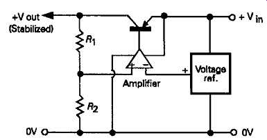
FIG. 24
Over-current protection systems:
A problem which is inherent in any series regulator system is that, in the event of an output short circuit, a very heavy instantaneous current could flow from the power supply reservoir capacitor through the pass transistor into the output. This will nearly always destroy the series device, since no simple fuse could operate rapidly enough in practice to rule out this type of failure. The simplest answer to this problem is to incorporate some rapid acting current-sensing circuit in the feed path to the pass device, which can be arranged either to 'steal' the input current to this transistor, as shown in FIG. 25a or to disconnect its drive, as shown in FIG. 25b. Frequently, such a current limiting circuit will be arranged to be 're entrant' in its operating characteristics, as shown graphically in FIG. 26, so that the output current which the pass device is allowed to deliver is related to the voltage existing across this device, which will limit the thermal dissipation of this device in the event of a sustained short circuit. This will also prevent the possibility of 'secondary breakdown' -- a failure mechanism which operates if the boundaries of the permitted area of current flow and collector voltage, shown for a bipolar power transistor in FIG. 27, are exceeded.
Practical series regulator circuitry
Some simple series voltage regulator circuits, which could, if necessary, incorporate current limiting systems, are shown in FIG s 28-31. All of these require some sort of voltage reference arrangement with which the output voltage from the regulator circuit can be compared. The simplest traditional type of layout used for this purpose is that shown in FIG. 28a, where an amplifier transistor, Qh is connected with its base fed from a potential divider (RVX and/^), connected across the output of the regulator, while the emitter of Q1 is held at a fixed potential by the zener diode, D. If the output voltage tends to increase, the current flow through R2 will increase, and the base voltage of Q2 will be lowered: an action which will reduce the regulator circuit output voltage again.
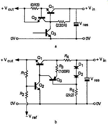
FIG. 25 Over-current limiting circuits (max = 2A)
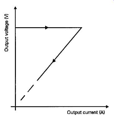
FIG. 26 Re-entrant over-current protection
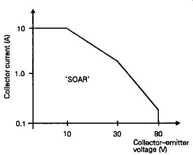
FIG. 27 Typical power transistor safe operating area rating (SOAR) . Collector-emitter
voltage (V)
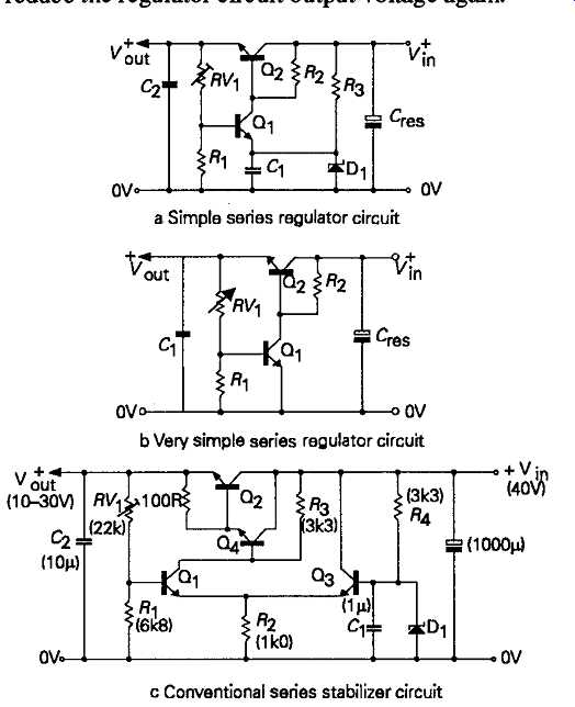
FIG. 28 --- a. Simple series regulator circuit ; c. Conventional series stabilizer
circuit
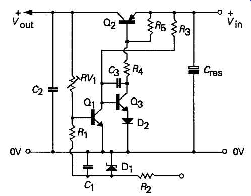
FIG. 29
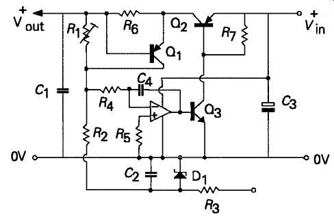
FIG. 30
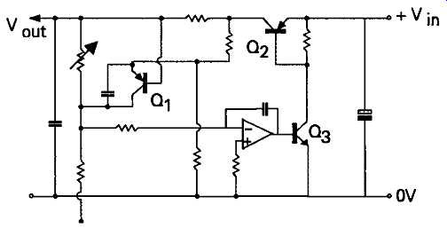
FIG. 31 Elaboration of circuit FIG. 30 to provide re-entrant current limiting.
The most immediate practical problems with this layout are that, while the output voltage can be adjusted by altering RVX, the lowest possible output voltage is V(£>{) + Vbe, (Q^, and it’s not possible, with any value of RVX, to adjust the output voltage down to zero. This circuit can be further simplified by dispensing entirely with the zener reference source, as shown in FIG. 28b, where the forward base-emitter potential of Qx is used as the reference. This arrangement works quite well, and allows the output voltage to be adjusted down to about 0.6V, but its regulation characteristics are poor because output voltage errors are also attenuated by the output potential divider (RVl and R!), which limits the ability of the circuit to correct these.
The output voltage control performance of the circuit can be improved by elaborating the input error comparator into a long-tailed pair configuration, as shown in FIG. 28c, where the zener diode has only to supply the base current of Q1, and the emitter impedance of Q1 is lowered by the emitter follower action of Q3.
All of the circuits shown in FIG. 28, suffer from the snag that the total base current required by Q2, which …can be quite large, must be supplied by R3. This leads to a voltage drop across R3, which, together with the necessary base-emitter potential for Q2, determines the minimum drop-out voltage for the circuit. If R3 has a large resistive value, this drop-out voltage will be large. If, on the other hand, R3 is made small to lessen this problem, the gain of the amplifying transistor, Q1 will be lowered, and the output voltage regulation factor, and the output impedance of the circuit, will be worsened. Moreover, at low or zero output currents from the circuit, all of the current flowing through R3 must be drawn off by Qj, so the current handling capacity of Q1? and its thermal dissipation characteristics, must be adequate.
In the case of the simpler circuit of FIG. 28a, under zero output current drain, the bias current not required by Q2 must also pass through the zener diode, so it too must have adequate current handling capability.
The use of a Darlington connected pair, as shown in FIG. 28c, will reduce the current handling capacity necessary for the control voltage handling stages, which will improve their gain, and the performance of the circuit. The snag, here, is that this will also tend to increase, somewhat, the drop-out voltage of the pass transistor.
An alternative layout, using the pass transistor in its inverted mode, is shown in FIG. 29. In this circuit, the input potential divider, RVXIRV is taken to a negative voltage reference source ( R2,Q1,C1), so that, if the output voltage from the regulator circuit is inadequate, Q1 is cut off, and the current flow through R3 causes both Q2 and Q3 to be turned hard on. Since the output voltage under these conditions will exceed that which is required, the potential now present at Q1 base will cause Q1 to conduct, and draw of f current which would otherwise flow through R3 into the base of Q3, causing the output voltage to be held at the required level.
Although the pass transistor is now operated in its common emitter, rather than its common collector (emitter follower) mode, and therefore offers a relatively high output impedance, all three of the transistors are operated as amplifiers, which gives a high regulator circuit open-loop gain, which reduces the circuit output impedance.
Advantages offered by this type of circuit are that the drop-out voltage can be very low, since the forward bias for the pass device is drawn from the OV line; that the zero output current flow through Q3 (and through the base-emitter path of Q2) will be zero, so that the dissipation of Q3 needs only to be that required by the base current of Q2 to provide the regulator circuit output current; and that the output voltage can be adjusted down to some 0.6V, as in FIG. 28b, but without the penalty of the relatively poor regulation factor offered by this layout.
An elaboration of this layout, due to the author (JLH. Wireless World, Jan. 1975, pp. 43-45), uses an operational amplifier in place of Qh which allows a further improvement in the precision of the output voltage control, and is shown in FIG. 30. In this the output voltage is adjustable down to within a few millivolts of zero volts, and the drop-out voltage -- the minimum practicable regulator voltage drop between supply and output potentials -- is less than IV. This circuit also uses Q1 in a current limiting arrangement, in which, on excessive output current demand, the power supply output voltage is progressively reduced, making it operate as a constant current source, but with the same degree of output noise and ripple rejection as it would possess in its normal constant voltage mode. The circuit can be made to operate in a re-entrant mode, if required, by connecting Q1 emitter to a tap on a further potential divider, as shown in FIG. 31, or, in the case of a more conventional circuit, as is shown in FIG. 32.
Voltage reference systems:
The use of a simple zener diode, or merely the forward base-emitter turn-on voltage for a junction transistor, have been employed, in the circuits so far described, as the reference voltage against which the regulator output voltage is compared to establish the required output level. All of these, however, are somewhat temperature sensitive, though it’s possible to temperature compensate an avalanche-type zener diode (i.e. one having a breakdown voltage in excess of some 6V), which will have a positive temperature coefficient, by connecting it in series with one or more forward biased silicon junction diodes, which will have a negative temperature coefficient. Indeed, temperature compensated zener diodes, such as the 1N821/1N827, are available, with a typical reference voltage of 6.2V, and a temperature coefficient as low as 0.001 %/°C. An alternative approach, and one which is used to provide a temperature stable voltage reference in al most all of the integrated circuit voltage stabilizer blocks, is to use a 'band-gap' arrangement.
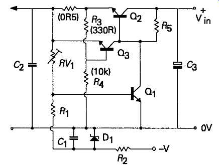
FIG. 32 Elaboration of circuit of Fig. 28b to provide re-entrant current
overload limiting.
The band-gap voltage reference circuit:
The use of a temperature compensated zener diode, with an output voltage of, say, 6.2V, would lead to some design difficulties in voltage stabilizers which were required to have an output voltage of, say, 5V. Also, all zener diodes have a significant noise component in their output voltage, and this would also appear in the output voltage of the regulator. For these reason s, the voltage against which the regulated output voltage is compared is normally derived from a band gap reference system. This type of circuit derives its name from the energy-band gap of the semiconductor material, at 0°Kelvin, which, for silicon, is 1.205V.
If, as in the circuit of Fig. 33, two identical transistors, Q1 and Q2, are operated at substantially different currents -- perhaps so that that through Q1 is ten times greater than that through Q2 -- there will be a voltage developed across R2, in the emitter circuit of Q2, which is equal to the difference between these two base-emitter voltages (defined as AVbe). This potential difference has a positive coefficient of voltage against temperature, and provides a means for generating a reference voltage which has a near zero temperature coefficient. The way by which this can be done can be seen from Fig.33. If the current gain of Q2 is sufficiently high that its base current flow can be neglected, the voltage developed across R3 will be ( R3/ R2)??^6. The total voltage across the circuit, from Q3 collector to the OV. line, will be, if Q3 is identical to Q1 and Q2, Voui = VbQ + (R3/R2W be and if these two component voltages -- one with a positive and one with a negative temperature coefficient -- add up to the band-gap potential of 1.205V, then the output voltage will have a zero temperature coefficient.
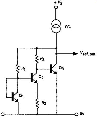
FIG. 33 Band-gap voltage reference circuit
IC voltage regulators:
The requirement for a zero temperature coefficient reference source is particularly critical in IC voltage regulators, since the voltage reference circuit will be contained within the IC package, and this package may become hot in use. A further point is that since all the silicon junctions are forward biased they will generate very little electrical noise. Also since the breakdown voltage of a zener diode is critically dependent on the doping level, and a selectively doped region of an IC chip would be inconvenient to arrange, and difficult to control to the required degree of precision, from the point of view of IC manufacture the more predictable behavior of circuitry using only forward biased junctions is much to be preferred.
The actual circuit layout used in most positive out put IC voltage stabilizers is of the general form shown in FIG. 34 -- which can be compared with the discrete component layouts illustrated in FIG. 28.
However, various circuit artifices are used to obtain performance refinements, such as the use of a low voltage drop constant-current source to feed the Darlington-connected output pass transistor pair to reduce the drop-out voltage, and to reduce the regulator IC output current if the chip temperature approaches its maximum permitted working level.
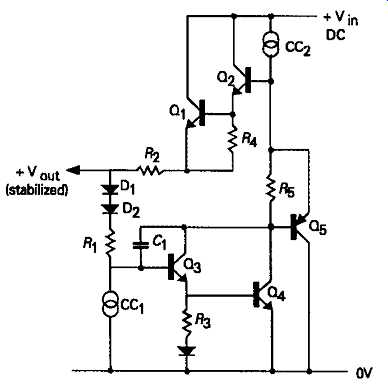
FIG. 34 Typical +ve input, IC voltage regulator schematic circuit
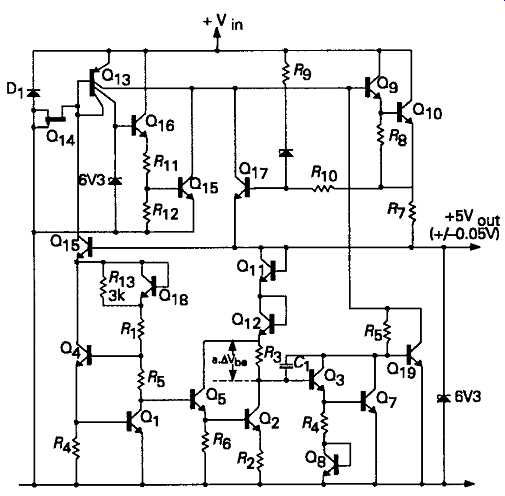
FIG. 35 Circuit layout of LM109 positive voltage regulator
For those who are interested, a detailed explanation of the way in which these internal circuit arrangements operate in a typical IC voltage regulator is given in Wireless World, March 1982, pp. 41-44.
The complete circuit of the LM 109 positive output three- terminal voltage regulator IC is shown in FIG. 35. Although this IC is designed to provide a fixed +5V output, its output voltage can be varied, above this figure, up to some +22V, by the use of the circuit shown in FIG. 36 -- an arrangement which is commonly used in adjustable voltage regulators, such astheLM317.
The use of adjustable output voltage regulator ICs in normal power supply applications, as distinct from their use as zener diode substitutes, has been made largely unnecessary by the availability of both +ve and -ve output fixed voltage regulators covering the range 5-24V, of which the most common types are those derived from the Fairchild 78xx and 79xx series.
These have now become so widely adopted as power supply components that discrete transistor voltage regulators are now only justifiable where output volt age and current requirements are outside the range available from IC systems.
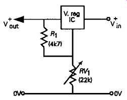
FIG. 36 Method of adjusting output voltage of fixed voltage regulator IC
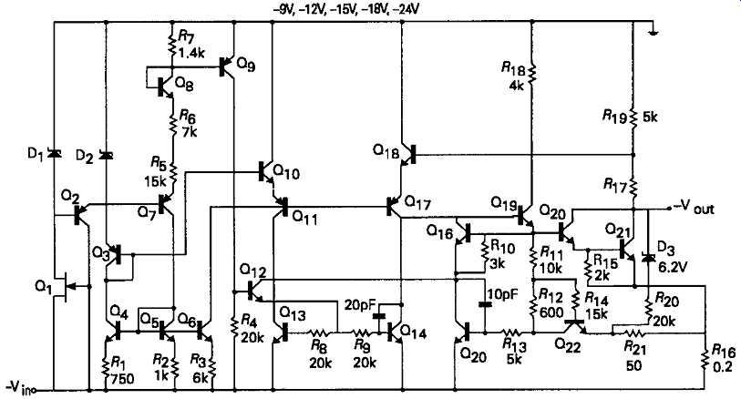
FIG. 37 Fairchild 79xx voltage regulator circuit
Because of the difficulty of fabricating good quality PNP transistors in ICs, the negative output voltage regulators, such as the µF79?? devices, employ a pass transistor layout which is similar to that shown in FIG. 29, with the output taken from the pass transistor collector. The band-gap voltage reference circuit still uses NPN transistors, referred to the -ve line, with a DC amplifier (Q6, Qn , Q14 and Q17) employed to invert the DC control voltage for application to the pass devices. The circuit of the µF79?? voltage regulator is shown in FIG. 37. The use of the modified pass transistor configuration gives the 79xx type regulator an improved drop-out voltage (1.1 V) as compared with that of the 78xx positive rail regulator IC. The output noise figure (125-375µ\0 is, however, worse than that of the 78xx device (40 90µF), with the lower output voltage ICs having better noise figures than the higher output voltage equivalents. If a very low output noise figure is desirable, it’s worth remembering that the low output current ICs, such as the 78Lxx and 79Lxx devices have a noise output of only about one third that of their higher power equivalents.
Increased voltage and current ratings for IC regulators
The normal IC voltage regulator has an input voltage limit of 35V -- though the 24V output µF7824 and µF7924 ICs allow a 45 V maximum input voltage and there are some higher voltage devices available -- and this may be inadequate for some applications. In this case, the easiest way to improve the voltage and cur rent ratings is by hybridizing the IC with a few external discrete components.
For example, the maximum current rating can be extended by causing the IC to control a parallel connected power transistor, as shown in FIG. 38.
This layout takes advantage of the fact that an IC voltage regulator draws very little current when its output voltage slightly exceeds the predetermined out put voltage level. So by connecting the compound emitter follower circuit, Q1 ,Q2, in parallel with a resistor (R{) in series with the IC, the parallel high current transistor will only be forced into conduction when the IC input current reaches a high enough level to cause a 0.6V drop across Rv The output voltage can be adjusted, if necessary, by inserting a network R4, RV^, in the reference limb of the IC. This gives almost exactly the same precision of output voltage control, and input noise and ripple rejection as would be pro vided by the IC on its own. Over-current limiting can be provided for this circuit in exactly the same way as shown, in FIG. 25a, for a discrete component system.
A circuit allowing both a higher input and a higher output voltage to be controlled by a fixed voltage IC regulator, such as the µF7815, is shown in FIG. 39. In this, the input voltage to the 7815 is control led by the potential divider circuit ( R5, Re), and the emitter follower, Q2, while output current (and input current) is only drawn from the IC if the emitter voltage of Qj falls below 15V, which allows the output voltage to be adjusted down to about 14.5V by the setting chosen for RVV Over-current limiting is pro vided by the transistor Q3, which steals the drive current from the pass transistor if the voltage across Rd exceeds some 0.6V.
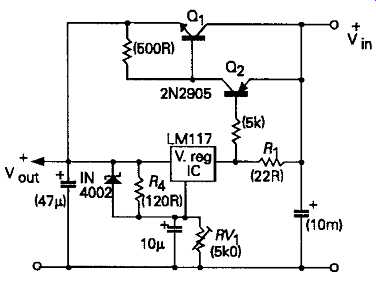
FIG. 38 Method of extending output current capacity of IC voltage regulator
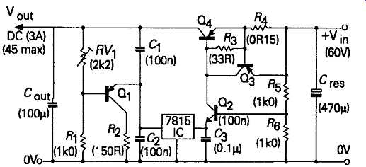
FIG. 39 Circuit providing increased current and voltage capability from IC
regulator
Switching and Switch-mode voltage regulators:
All of the voltage regulators examined so far have come within the category of DC to DC converters, in that they have taken a DC input; usually neither particularly clean, in terms of freedom from electrical noise and mains induced ripple, nor stable in voltage; and converted this into a stable, much more noise free, but rather lower output voltage, since the regulator required some internal voltage drop in order for it to operate. There are, however, other useful arrangements which allow, for example, an input source of one polarity, say +15V, to be converted into an output of the opposite polarity, say -15V, or, alternatively, which will allow a lower voltage, say +5V, to be converted into a higher voltage, say +15V. Since all of these systems rely on the transfer of the energy stored in a capacitor or an inductor from the input to the output circuit, by some repetitive switching action, these circuits are generally called 'switching regulators'.
There is also a specific category of switching power supply system in which the input DC source is just an input rectifier/reservoir capacitor circuit. This pro vides a high power, but rather rough DC supply straight from the raw AC line, and this is then converted into a stable DC output, isolated from the mains input, by a high frequency oscillatory switching circuit, coupled to a small high frequency transformer.
This type of circuit is employed because great savings in size, weight, and heat dissipation can be made by the use of high frequency, rather than 50-60Hz, volt age transformation techniques. The term 'switch mode' is usually used when referring to systems of this kind.
DC to DC reverse polarity converters:
One of the simplest DC-DC converter systems, for which circuits frequently appear in the 'Design Ideas' columns of electronics magazines, uses a free-running square-wave generator, such as, say, a 555 type IC, connected as shown in FIG. 40, to produce an output in which the charge stored in C1 on each +ve going half cycle, can be rectified by the diodes D1 and D2, and 'pumped' into the output circuit. By the choice of the polarity of D1 and D2, the DC output from the circuit can be either +ve or -ve.
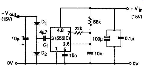
FIG. 40 Negative voltage generator circuit
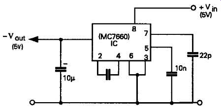
FIG. 41 Switching polarity inverter circuit
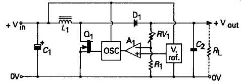
FIG. 42 Simple switch-mode regulator circuit
A more elegant switched-capacitor converter circuit, using the same philosophy, is that shown in FIG. 41, based on a MC7660 IC. This gives a polarity-reversed output voltage which is very close to that of the input, for supply voltages up to 10.5V, and for output currents up to 10mA. The overall conversion efficiency of this circuit is typically about 95%. Similar types of device are available from Texas Instruments, National Semiconductor, and many other manufacturers.
A point which must be remembered in any switching regulator is that it’s capable of injecting a significant amount of noise back into its own supply line, so the voltage feed to the circuit must be adequately decoupled.
A much better type of circuit is the kind in which the energy store is an inductor, in that, for a given physical size, the current transferred to the output can be much greater. A typical example of this kind of arrangement is shown, schematically, in FIG. 42, in which a switching transistor Q1 is used, alternately, either to permit or to interrupt the current flow from the input DC supply through the inductor, Lv to the 0V line.
When the current flow through Lx is interrupted, the voltage at the collector of Q1 will rise, very rapidly -- a phenomenon known as the 'back EMF', or, more popularly, as the 'flyback effect'. This causes the diode, Dv to conduct, and causes current to flow into the output load, RL. The output voltage provided by the circuit is then compared, through the voltage divider network, RVVRX, with a reference voltage, and the amplified difference used to control the mark-to space ratio of a high frequency oscillator. This, in turn, controls the switching characteristics of Q1, to regulate the output voltage.
Although bipolar junction transistors can be used, as Q1, in this application, power MOSFETs are more commonly used because they have a more rapid switching action and their high input (gate) impedance makes them easier to drive. By reversing the positions of L1 and Q1, as shown in FIG. 43, so that when the current flow through Lx is interrupted the voltage at its live end suddenly swings negative, the output polarity can be reversed, to allow a -ve output voltage to be derived from a +ve input supply line. As in FIG. 42, the output voltage can be controlled, quite precisely, by comparing the output level with a reference source, and using the amplified difference to control the on-to-off time duration (the mark-to- space ratio), of the switching transistor, Q1.
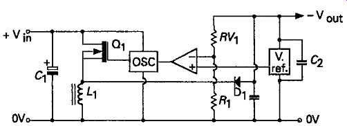
FIG. 43 Negative output voltage switch-mode regulator circuit.
Since the switching frequency can be made quite high -- say 100kHz -- the value of the output smoothing capacitor, C2, does not need to be very high to reduce the residual switching ripple to the required low level.
Both of these switched inductor circuits can provide an output voltage which is greater than the input supply line level -- say, -15 V out from a +5 V in -- and typical efficiencies can be as high as 90-95%, so that the system runs cool.
The control of the mark-to-space ratio of the wave form used to operate the switching transistor, in order to adjust the output potential provided by the circuit, can be done by the kind of circuit shown in FIG. 44. In this a free-running 'triangular' or sawtooth waveform generator is 'sliced' by a high gain voltage comparator IC, which gives an output waveform in which the relative durations of the +ve and -ve parts of the cycle can be altered with reference to one another. If necessary, this output waveform can then be sharpened up still further, to improve the efficiency of switching, by reducing the length of time occupied in the on to off transitions, by interposing a CMOS logic gate IC between the output of the comparator IC and the switching device.
Sawtooth generator:
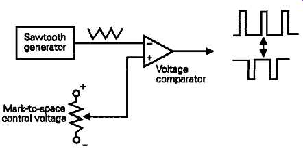
FIG. 44 Adjustable mark-to-space ratio oscillator circuit
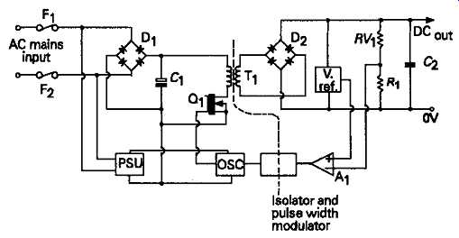
FIG. 45 Complete AC-DC switch-mode power supply
Switch-mode power supply (SMP) systems:
A typical layout for a switch-mode power supply is shown in FIG. 45. In this, the mains line AC voltage supply is rectified by the diode bridge (D1)and charges a capacitor (C1), to provide a DC source of either 163V or 340V, depending on whether the input supply line is 115 or 240V. Either this, or some alternative DC supply is used to power a pulse-width modulated oscillator, operating normally in the range 25kHz-200kHz, depending on the designer's choice, which controls the conduction of the switching transistor Q1. In the past, this would normally have been a bipolar junction device, but the growing availability of higher switching efficiency MOSFETs has made these the more attractive choice.
It’s nearly always essential to provide full electrical isolation between the mains input and the DC output lines in any power supply, for safety in operation, and to allow freedom in the choice of interconnections in the load circuit. In the case of an SMP supply, this isolation is given by the transformer Tx. Because of the high operating frequency of this system, this trans former need only have a small core cross-sectional area -- in practice this core will often be a 'ferrite' toroid -- and the windings need only few turns, so that they can be wound with relatively thick wire which gives a low winding resistance and a high overall transformer efficiency.
The rectified output voltage is used to power a DC voltage reference source, against which the output DC level can be compared. As in the previous systems, shown in FIGs 42 and 43, the error voltage detected by the amplifier (A) is used to operate a pulse-width modulator circuit which controls the conduction cycle of the switching transistor, Q1. However, in the case of an SMP, the control circuit must be chosen so that a further isolation element, usually either an 'opto-coupler' or a small pulse transformer, can be interposed in the control path between the error amplifier and the switching transistor.
The DC operating supply for the switching oscillator, and other low voltage electronic circuitry shown on the left-hand side of the isolating transformer, is most easily provided by a simple, very low power, transformer-rectifier circuit of conventional form, al though various ingenious schemes have often been used in commercial designs to provide a short burst of DC to this circuit, on switch-on, to allow the oscillator power supply, once the oscillator has started working, to be derived from a tertiary winding on T. Once again, since the 'ripple' frequency of the rectified supply is so high, only a small value reservoir capacitor (C 2) is needed to reduce this to an acceptable level. However, since the impedance of an inductor increases with frequency (ZL = 2 pi fL), even a low value inductor, with a very low DC resistance, interposed between the secondary rectifier bridge (D2) and the output capacitor (C3) and load, will give a substantial reduction in the output noise and ripple.
Because the SMP is so compact in size, and has such a low heat dissipation, this kind of power supply is now very widely used in 'desk-top' personal computers.
Also, because of the popularity of this type of circuit, both pulse-width modulator systems, and switched capacitor and inductor converters, as well as complete switch-mode regulator circuits are available in IC form, from a wide range of manufacturers, such as Harris, Hitachi, National Semiconductors, SGS, Siliconix, Silicon General and Texas Instruments.