AMAZON multi-meters discounts AMAZON oscilloscope discounts
Introduction
Most linear circuit design is based on the convenient, and simplifying, assumption that the system will be noise free -- that the end result of any amplification, filtering, or other signal handling processes will be the signal on its own, attenuated, enlarged, or modified as a result of the stages through which it has passed, but free from any alien signals not presumed to be present in the input, and not wanted in the output.
Sadly, in reality, this desirable situation can never exist, and wanted signals are always contaminated, to some extent, by unwanted electrical intrusions of one kind or another. For example, this pollution of the desired signal could be due to hum pick-up from the 50 or 60Hz mains power supply network, almost al ways found within buildings -- even when a mains voltage supply is not used to power the equipment concerned -- or to unwanted feedback of signal components; usually via the supply lines; from the output into the earlier stages of the system. In addition, all electrical input signals, and the output of all electrical signal handling circuitry, will be accompanied by noise. This may be externally generated, from a variety of sources, such as atmospheric electrical discharges, or from man-made, and usually impulse type, interference arising from such things as fluorescent lighting installations, thermostat switch-gear, or petrol engine ignition systems. Noise will also exist within the system itself as a fundamental characteristic of the basic physical nature of the signal source and all the associated electronic circuitry.
All of these unwanted noise signals can, to some extent, be lessened, or made less obtrusive, by care in the circuit design and in the layout and construction of the equipment, and it’s therefore desirable for the designer to keep in mind the nature of noise sources so that he can come closer to the ideal result of a noise free output signal.
The physical basis of electrical noise
Thermal or Johnson noise (resistor noise)
At all temperatures above absolute zero, (0°K or -273.15°C) the electrons present in any conductor are in a state of restless random movement, which leads to the statistical probability that, at any given moment, there will be more electrons present at one end of a conductor than the other, a situation which causes a fluctuating electrical voltage to be developed across the conductor. This noise voltage will increase as the temperature is raised, since this increases the degree of agitation of the electrons, and as the resistance of the conductor is increased -- because the electrostatic attractions which tend to oppose the movement of charges away from their rest condition of uniform distribution are lessened by the isolating effect of electrical resistance -- and as the bandwidth over which the noise signal is measured is increased.
The mathematical relationship between these effects, originally defined by Johnson -- hence the term 'Johnson' noise -- is usually expressed in the form:
en(rms) = √[4kT Δ f R] (1)
... where en is the mean noise voltage, normally defined as volts per √Hz, k is Boltzmann's constant (1.38 x 10^-23), T is the absolute temperature, in °K, Δ f, is the measurement bandwidth, and R is the resistance of the conductor, in ohms.
The probability that there will be an imbalance in the charge present between the two ends of the conductor is an essentially random one, which leads to the wideband noise characteristic of this voltage. Similarly, the instantaneous magnitude of this imbalance is also entirely random in nature, which means that the noise voltage distribution has a 'Gaussian' characteristic curve, as shown in FIG. 1.
Amplitude:
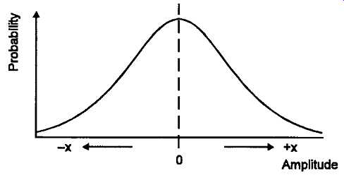
FIG. 1 Gaussian noise peak amplitude distribution curve.
It can also be seen from equation (1) that the energy distribution of thermal noise, as a function of frequency, is constant, per unit bandwidth -- a characteristic which is given the descriptive term 'white' noise. By the use of this formula, it’s a simple matter to plot a graph of the thermal noise level associated with any value of bandwidth, ambient temperature and source resistance. A typical set of curves relating noise voltage to source resistance for various bandwidths (20kHz is included as the nominal bandwidth of the audio spectrum) and an ambient temperature of 25°C (298.15°K) is shown in FIG. 2.
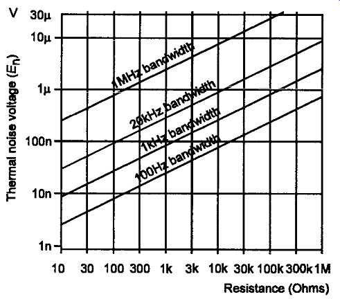
FIG. 2 Relationship between thermal noise voltage and circuit resistance
(at 25°C)
Resistance (Ohms):
There are other sources of electrical noise, but Johnson noise is an invariable feature of any system which contains resistive elements, whether these are associated with the signal source or with the circuitry and active devices which are connected to it.
Shot noise (Current flow noise)
Another important source of noise which is an inherent feature of all electrical circuitry is 'shot' noise, which is characteristic of all current flow. Whether current flow is due to the motion of ions or electrons, it is, by its nature, discontinuous and particulate, with units of charge arriving individually at their destination in a random pattern. In very large current flows, this random time interval separating the arrival of any one unit of charge from the next will be less than that in the case of smaller current flows, but it will still be particulate in its nature, like lead shot falling into a receptacle.
This means that the total noise current will increase with current flow, but the scatter of the individual noise pulse amplitudes will increase as the current decreases. Like thermal noise, this is white noise, with a constant energy per unit bandwidth, but it is, in this case, related solely to current flow, and is independent of both ambient temperature and the resistance of the conductor.
The relationship between current flow and shot noise (current) can be expressed by the equation …
I_n = √2 I_dc Δ f (2)
where I_n is the noise current, in amperes (independent of source impedance), q is the charge on the electron (1.6 x 10^-19 coulombs, where one coulomb is an ampere second), Idc is the current flow, also measured in amperes, and ^i s the measurement bandwidth.
A further source of noise, having similar characteristics to shot noise, is found in those components, such as tetrode or a pentode valves, in which the internal current flow is offered a choice of destinations. This is known as 'partition noise'. This particular mechanism is not of particular importance, in the case of solid state components, except that some integrated circuit constructions employ, as a matter of circuit convenience, multiple collector transistors, which will, because of the existence of partition noise, be significantly noisier in operation than single collector devices. However, in addition, majority and minority carrier recombination effects in bipolar transistors do give rise to a similar type of noise mechanism.
Flicker, excess or 1/f noise (defect noise)
These are terms given to a further type of noise which will arise within a resistor or a semiconductor, or any other conducting material, when a potential applied across it causes a current to flow. This effect is due to the inevitable existence of irregularities and imperfections within the material from which any conducting component is made, and was first observed as a 'flicker' type variation in the electronic emission from the surface of the cathode of a thermionic valve. Like partition noise, these defects offer a choice of paths for current flow, but with the difference that both the total resistance and the transit time for these paths will fluctuate, from one instant to another, giving rise to an additional noise voltage superimposed on the current (shot) noise, and the existing thermal noise of the resistive path.
Although a mean value of 'excess' noise can be determined, for any given component type, by laboratory measurements made on a sufficiently large number of nominally identical devices, it’s impracticable to define it by any simple mathematical relationship which would be applicable to all circumstances, al though in general form the power spectral density of this noise component follows the relationship ...
Ρ_f ω (rms)=Κ I α ωΡ (3)
where K is some constant appropriate to the manufacturing process and materials used, ω is the frequency in radians/s, alpha = 2, and ß = 1.
This type of noise is a low frequency phenomenon, which is principally noticeable at frequencies below 1kHz, and which increases as the frequency is lowered -- a characteristic which has given rise to the common description 1/f noise. (This type of noise frequency distribution is known as 'pink' noise, to distinguish it from the wideband, uniform energy distribution 'white' noise).
This kind of 1/ f noise effect is found in resistors, as a result of mechanical imperfections in their manufacture, such as variations in the uniformity of the con ducting path, or in the integrity of the attachment of the connecting leads to the resistor body. This is the principal reason for the lower noise figure of metal film resistors in comparison with carbon composition types.
Contact noise has similar l/f characteristics to that of excess noise, and is due to the breakdown of insulating films of surface contaminants present on contacting conductive faces, or to the interruption of minute current paths within the material. This is the reason for the lower noise of welded or soldered contacts, in comparison with 'crimped' end-caps, on, for example, wire wound resistors -- welded or soldered connections are not practicable with film-type components.
Typical mean (rms) values of excess noise in different resistor types are shown in TBL. 1, in uV/V (i.e., measured at a current flow of 1mA through a resistor value of 1k-ohm), with a measurement bandwidth of 30-300Hz. (The measured values have been corrected to allow for thermal noise.)
A similar type of noise occurs injunction transistors, due to surface recombination effects within the base region, and is one of the reasons why a PNP type transistor (which has an N-type base region), will usually have a lower noise figure than an NPN one. 1/f noise also occurs in junction FETs, and MOSFETs, due to reverse gate-source leakage currents. Most data sheets for low-noise transistors and ICs will show graphs of the l//noise characteristics of the devices in question.
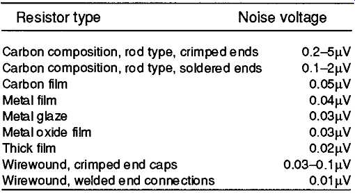
TBL. 1 Excess noise in different styles of resistor
A typical noise characteristic for a low-noise opamp IC, illustrating this typical 1/f behavior, is shown in FIG. 3.
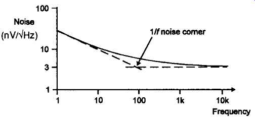
FIG. 3 Flicker noise characteristics of typical low-noise opamp.
Noise figure or noise factor:
There are several ways by which this can be defined, but probably the simplest is to regard it as the extent to which the imperfections of the component or circuit in question degrade the signal/noise ratio of the system -- measured in dB. This avoids the intellectual pitfall of thinking -- as, for example, in the case of the data quoted for the BC322, a low-noise PNP transistor, whose 'noise figure', as a function of generator resistance, is illustrated in FIG. 4 -- that a lower system noise could be obtained by choosing a low collector current and a high source impedance. In reality, the only bargain that is offered is that if the generator resistance is made high enough, the thermal noise of the source will swamp the thermal, shot and flicker noises due to the transistor -- which flatters the performance of the transistor but actually frustrates the designer's original intentions.
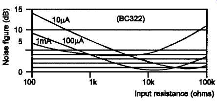
FIG. 4 Noise figure for low-noise PNP transistor as a function of input circuit
resistance and collector current.
If the generator impedance is, or can be made, low enough that the thermal noise from this source is already very low, the best design approach is to choose a transistor whose noise figure is acceptably low at a level of collector current which is appropriate for the chosen input impedance.
Low noise circuit design
Noise models for junction transistors and J-FETs
The easiest way to visualize the practical effect of the various noise components which can arise in an amplifier circuit is to assume that one has an ideal noiseless device, in which the noise signals, due to the various physical mechanisms operating within the de vice, are represented by voltage or current noise generators connected to its input. The magnitude of these noise signals, referred to the input, is then measured by dividing the noise output voltage by the stage gain.
For example, in the case of the bipolar transistor circuit, illustrated in FIG. 5, the voltage noise, en, referred to the input, will be the RMS sum of the thermal noise generated by the resistive components present in the transistor base circuit, as well as the shot noise resulting from current flow through the base emitter region, and the flicker noise due to lateral current flow within the base region. These input resistive components consist of the base spreading resistance, Rfo (that resistive component, effectively in series with the base connection, due to the resistance of the lateral current path from the base connection to the active part of the base-emitter junction), and the base-emitter 'bulk resistance', Ree, (representing the bulk resistivity of the base-emitter junction region --which will usually be less than Rbb by at least a factor of 10).
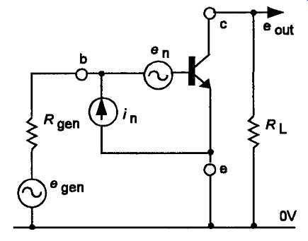
FIG. 5 Junction transistor noise model
In FIG. 5, the sum of these voltage components is represented by an idealized zero impedance voltage generator, en, in series with the input circuit. In practice, shot noise in the transistor will be reduced, as seen in equation (2), if the transistor is operated at the lowest practicable collector current, and flicker noise will be minimized if the transistor is operated at the lowest sensible collector voltage.
There are also input noise current components, rep resented in FIG. 5 by the current generator, /n, assumed to offer an infinitely high source impedance, connected in parallel with the input base-emitter circuit. These noise current sources arc the shot noise components of the base current, and the modulation of this base current by flicker type effects. These noise sources can again be minimized by operating the transistor at its lowest practicable collector current, and by choosing a transistor with a high current gain, since both of these actions will reduce the base current of the device.
From the point of view of amplifier performance, very little can be done to minimize the effect of any voltage noise, en, which is due to the device, since this will appear in series with any input signal voltage. The main options open to a designer seeking the best possible s/n ratio arc to choose the best device type which is economically available, or to arrange that the input generator voltage is large in relation to the input voltage noise of the amplifier.
Current noise, I_n, is important because the flow of this current through the input (generator) impedance will give rise to a noise voltage. If the generator impedance is high, and cannot be reduced, a better noise figure can, perhaps, be obtained by using a junction FET as the amplifying device, as illustrated in FIG. 6, since this type of transistor has a very low gate leakage current, and therefore a low value of input noise current, I_n.
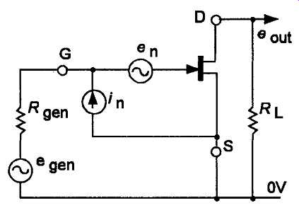
FIG. 6 Junction FET noise model
(Note. Thermal noise is a feature of the real (i.e. resistive) part of a circuit impedance. However, in the case of a noise voltage which arises because of the flow of a noise current through an input impedance, the reactive (i.e. capacitive or inductive) parts of the input impedance must also be considered.) On the other hand, junction FETs usually have a relatively large voltage noise figure, en, because the conducting channel length of a typical small-signal J-FETs, and therefore its effective thermal noise resistance, is substantially greater than the emitter-collector path length of a bipolar junction transistor. This noise voltage due to the FET channel can be defined by the equation:
en(rms)=√4kTRnΔf (4)
…where Δf is the measurement bandwidth, k is Boltzmann's constant, T is the absolute temperature, °K, and Rn is the effective channel resistance, and in typical devices is approximately defined by:
Rn = 0.67/g_fs (5)
…where g_fs is the FET common-source forward trans conductance.
In the flicker noise region, the mean value of the noise component en is approximately defined by the equation:
en(rms) = √4kRn Δf(2^-f1/f_Beta) (6)
... where f1 is the upper corner frequency of the flicker noise, and ß has a value between 1 and 2, depending on the process by which the device was made, and the purity and homogeneity of the semiconductor slice.
The combined effects of these noise sources, at low frequencies, is illustrated in the graph, due to Siliconix (Application Note 74-4), shown in FIG. 7.
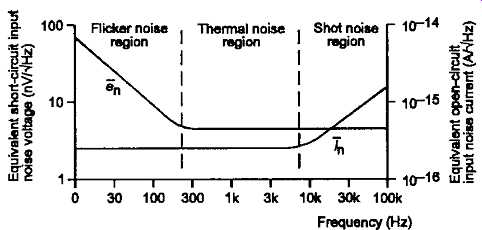
FIG. 7 Junction FET noise characteristics --- nicker noise , Thermal noise
. Shot noise region I region; region Frequency (Hz)
Since the channel resistance is related to the trans conductance of the device, the noise voltage, en, can be reduced by increasing the forward transconductance of the device, gfs, which can be done by parallel connecting two or more identical FETs -- in numerical terms, this will reduce en by IHN if T V devices are connected in parallel.
A similar result is given if the FET gate area is increased, which increases the channel area, and also reduces channel resistance. However, both of these measures increase the input (drain-source), and the feedback (drain/gate), capacitance of the FET. FETs also suffer from a type of input noise current, called 'burst' or 'popcorn' noise (because of the sup posed similarity of the noise produced in an audio system to that of corn popping during roasting). This occurs particularly at low frequencies (10Hz or below) and is presumed to be a type of contact noise affecting the aluminum gate metallization (Observation has shown that it’s made worse if the surface of the semiconductor die is known to have been contaminated prior to the metallization process.) Although still present to some extent in all junction FET amplifiers, modern devices are much less affected by this defect.
Increasing the reverse bias of the FET gate/channel junction will reduce the input gate capacitance, but will -- up to the point of cut-off -- somewhat worsen both flicker and popcorn noise, as well as the thermal noise voltage associated with the channel, since the resistance of this will also be increased by increasing the reverse bias.
The operational amplifier model
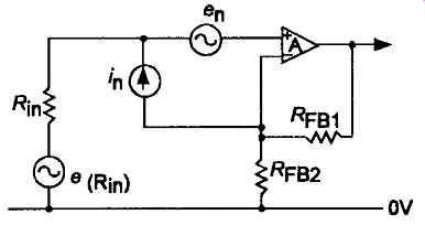
FIG. 8 Operational amplifier noise model
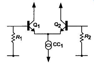
FIG. 9 Input long-tailed pair layout
The opamp circuit, shown schematically in FIG. 8, presents a very similar situation to that of a junction bipolar transistor or FET circuit, since the opamp input stage devices will be either transistors or FETs. However, because the input stage will almost invariably consist of an input long-tailed pair configuration, of the kind shown in FIG. 9, if the two input transistors are physically identical, as is usual, all the input device noise contributions will be worsened by a factor of √2 (3dB), by comparison with the single-ended layouts shown in FIGs 5 and 6.
The equivalent input noise resistance due to the source and feedback resistors, shown in FIG. 8, and associated with any practical opamp. circuit layout, can be determined from the equation:
Req = R2in + [] (7)
…in which the symbol I I denotes parallel connection (i.e. ^fbi^nW^fbi + ^ftß))
The equivalent input noise resistance defined by equation (7) is also applicable to single-ended stages where negative feedback is applied, for example, from the output to the emitter or source of a junction transistor or FET, but with the complicating factor that Rfb2 will, in any case, modify the noise figure and stage gain of the device.
MOSFETs
These have very much worse noise figures at low frequencies than either junction FETs or bipolar transistors, mainly due to flicker noise and popcorn noise phenomena. It seems probable that the major cause of MOSFET flicker type noise is the continuous creation and recombination of charges from the neutral charge pairs constituting the conductive channel, but some of this noise may be due to the on-chip protective zener diodes.
Because of their poor LF noise figure, MOSFET devices are seldom used for DC amplifier or low frequency low-noise applications, except where the extremely high input impedance typical of a MOSFET is an essential requirement -- as For example in ionization chamber amplifiers. (In those MOSFETs in which the gate is not protected by an integral zener diode, input resistances of the order of 10^15 ohms are obtainable.)
(Note. It should be remembered in this context that small signal junction FETs can offer an input resistance which is typically greater than 10^12 ohms, and are also free from proneness to damage due to electrostatic breakdown.)
Amplifiers for very low impedance systems
Bipolar transistor systems
The growth of interest in low-noise amplifiers for use with low impedance, low output voltage sources, such as strain gauges, thermocouples, and, in the audio field, moving coil gramophone pick-up cartridges (whose output voltages, for a lcm/s. groove excursion velocity, may be as low as 50-500µ\0, has encouraged the semiconductor manufacturers to develop very low noise devices, frequently packaged as matched dual transistor pairs, specifically intended for use with input configurations of the kind shown in FIG. 9.
In order to achieve low amplifier noise, all of the transistor internal noise components must be of a low level, and, in particular, its thermal noise resistance, referred to the input, should be no greater than that of the signal source. The effective internal resistance of the transistor can be lowered either by choosing a device with a large base/emitter junction area, such as a medium power device, or by parallel connecting a number of low-noise small-signal transistors. How ever, in practice, such transistors must either be closely matched in their base-emitter current threshold (diode) voltage or an emitter resistor (R^ must be inserted as shown in FIG. 10, to ensure that the total collector current is equally shared -- and these added resistances will worsen the thermal noise figure of the circuit.

FIG. 10 Use of bipolar transistors connected in parallel to reduce input
noise resistance of circuit
One of the earliest semiconductor designs aimed at the solution of this problem was the National Semi conductors LM194/394 'super-match pair'. This is essentially a multiple device integrated circuit in which two groups of parallel connected, and notion ally identical, transistors have been fabricated, in a manner which gives a random distribution across the semiconductor chip to even out any differences between one group and the other.
Because of the multiplicity of parallel connected transistors, the base spreading, Rbb>, and the bulk, Ree/, resistances are very low, at 40 and 0.4 ohms respectively, which means that the thermal noise voltage, due to the internal resistance of each half of the transistor pair, is kept to a very low level.
The optimum noise figure for any transistor amplifier requires that the collector current, I_c, should be chosen to give the best performance for the known input (generator) resistance. In general, this value of I_c would be determined by reference to the manufacturer's data sheet, or by the choice of a transistor for which this value was known.
Typically, the relationship between the noise figure, collector current and source resistance will be defined by the use of a diagram of the kind illustrated in FIG. 4. However, for a transistor, such as the LM194/394, whose behavior approximates very closely to the ideal model, the base current shot noise, I_n, can be fairly accurately predicted from the equation in (rms):
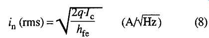
(8)
…and the optimum collector current, for each half of the long- tailed pair, can be derived from the relationship:
…where q is the charge on the electron, and I_ife is the small-signal, common emitter current gain of the transistor, and rs is the generator resistance.
With any real-life device, there will be also some flicker noise at frequencies below about 1kHz, and this will be a function of the manufacturing process, and therefore unique to the device in question. That for the LM194 is shown in FIG. 11.
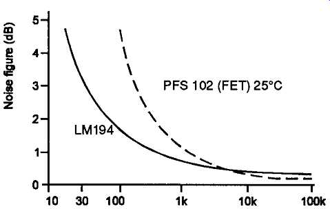
FIG. 11 Noise figure ofLM194, compared with that of a low-noise FET as a
function of input resistance.
In recent designs, improved manufacturing techniques have allowed even better noise figures to be obtained than those given by the original LM194/394 super-match pair, with components such as the PM, MAT02, and more recently still, the SSM-2220 and SSM-2221, PNP and NPN matched pairs, from the same manufacturer, all of which have noise voltages (with zero external input resistance) of less than InV/VHz over the frequency range 10Hz to 100kHz.
A typical ultra-low-noise circuit design, intended for use as a strain-gauge DC amplifier, is shown in FIG. 12 (National Semiconductors Application Note AN-222-7).
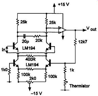
FIG. 12 Strain gauge DC amplifier design using LM194 super-match pair transistors.
Thermistor -15 V
Junction FET designs
As noted above, junction FETs will, by their nature, generally have a higher input thermal noise resistance than bipolar junction transistors and will therefore be of greatest value in systems designed for use with higher source (generator) impedances where the noise current associated with the amplifying transistor is more important than the device thermal noise voltage.
With the best available devices, the 'crossover' input impedance, above which the junction FET will offer a lower noise figure than the best available bipolar transistor, is of the order of Ik ohms. Above this figure, the better linearity, and greater tolerance of input overload of the J-FET may offer useful performance advantages.
The effect of the distribution of stage gains
In multiple stage circuitry, where every stage will contribute some noise to the final total, it’s desirable to arrange that as much signal gain as possible is obtained in the early stages of the system, so that the signal level at later stages of the circuit will be high enough to swamp the noise voltages due to these stages. The effect of stage gain on overall circuit noise can be expressed by the equation …

where En is the total noise voltage at the output of a multi-stage system, N1, N2, N3 ... Nx are the noise voltages, referred to the inputs, of stages 1, 2,3 ... to X, of the system, and a, ft, c ... x are the stage gains of these stages.
If the magnitudes of the early terms in this series can be made sufficiently large, for example, by making the stage gains of the early stages high enough, the noise voltages contributed by the later parts of the circuit can be ignored. Since it’s assumed that the design of the circuit will be chosen so that the noise figure of the early stages is as low as possible, care must also be taken to avoid signal loss, such as by input attenuation prior to amplification.
Summary
In order to attain the lowest thermal noise figure in a given stage, the circuit should be chosen to employ the lowest practicable values of circuit resistance (and input impedance, where there is a significant input noise current) compatible with satisfactory circuit performance in other respects. However, one must bear in mind that it’s not profitable to design for a low amplifier input resistance, in the pursuit of the lowest possible level of circuit noise, if this results in a mismatch to the generator output impedance, and a consequent loss of input signal voltage. So make sure, prior to deciding on the circuit design, that the optimum load resistance is known.
Where a very low noise level is essential, constructional techniques and components of the best available type and quality should be used, and if active devices are to be employed, then the maker's data sheets should be consulted to discover the best values of operating current and voltage for these devices, for the intended input circuit resistance.
With junction transistors, if the data sheets suggest a range of operating currents which apparently give similar device performance for a given source impedance, choose an operating value at the lower end of this range, since it will be associated with a lower level of base current shot noise.
Also choose transistor types having a high value of current gain, since they will have the lowest level of base bias current for a given collector current, and consequently the lowest level of input current noise, and they should be operated at the lowest sensible level of collector voltage commensurate with the likely level of output voltage swing that the stage will be required to handle, because this will minimize the leakage currents, and the flicker noise level associated with these.
With J-FETs, in which, at low frequencies, the input noise currents are usually exceedingly low, the best noise performance is likely to be obtained with circuits in which the input resistances are relatively large (of the order of 1k-ohms or greater). Unlike bipolar transistors, J-FETs show lower device noise figures at the upper end of the normal drain current range -- because this is associated with lower channel resistance values, and consequently lower levels of the input thermal noise voltage associated with this. Obviously, it’s desirable to keep the operating temperature low, since thermal noise is associated with circuit temperature.
However, there is not usually a lot that the designer can do about this, and, in any case, the performance, of most semiconductor devices worsens, either in respect of gain figures or in terms of leakage currents, if they are used at temperatures outside the normal ambient temperature range.
The final point to remember is that all noise problems are worsened if the system bandwidth is in creased -- remember the old adage that 'the wider the window, the more the dirt flies in -- so make sure that the working bandwidth is not wider than necessary for proper circuit operation. Judicious filtering or band width limitation can be greatly helpful in preserving a good signal to noise ratio.
Noise from external sources
With any high gain amplifier, especially if it has a high-input impedance, and a wide bandwidth, there is a tendency for externally generated wide bandwidth impulse-type noise to break through into the signal channel. There are many mechanisms by which this can happen, of which the most common is by direct pick-up by the amplifier unit itself, or by its input leads, if these are inadequately screened, or if the screening (usually provided by a woven metallic braid on the outside of the cable, or by the use of a conductive, usually metallic, enclosure housing the input components) is not connected to the common OV line by a sufficiently low impedance path.
Alternatively, electrical impulse-type noise signals may be carried into the enclosure housing the amplifier -- even when this is properly screened -- by the mains power cable, and by the power supply transformer primary winding, particularly if the transformer is unscreened. Direct pick-up of impulse noise signals by the internal input connections can occur from both of these sources, and it may be necessary either to employ some form of mains input low-pass RF filtering, such as that shown in FIG. 13, or to house the power supply unit within a separate enclosure, to reduce interference pick-up to an acceptable level.
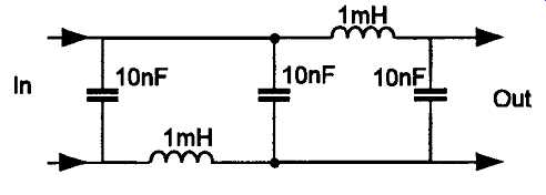
FIG. 13 Mains input RF filter.
Breakthrough from the mains input on to the internal DC power supply lines can occur, but is unusual, since these DC rails are nearly always well decoupled to the common 0V line by low impedance by-pass capacitors. The sensitivity of all electronic systems to interference pick-up is related to the pass-band of the system. Once again, the wider this is, the worse the problem will be.
A particular problem with amplifiers employing negative feedback is that these can show an exaggerated sensitivity to impulse-noise pick-up, if, by mal function, or by an error in design, the feedback loop has an substantially reduced stability margin, and a consequent tendency to sporadic oscillation -- especially if this occurs at some relatively high frequency.
Radio pick-up
This is an annoying phenomenon which can often occur in prototype systems, and is most noticeable in audio amplifiers, where even a low-level radio signal break-through can be very obtrusive when present under 'zero signal' conditions. This problem can have many causes, but is usually due to pick-up on input connecting leads-particularly if imperfectly screened or if the screening is inadequately earthed -- and to needlessly wide bandwidth input stages.
It’s often suggested that poor quality soldered joint connections can provide the necessary (Schottky diode type) rectification of an input RF signal to allow the LF modulation to be separated from the RF carrier of a radio signal, which allows these LF components to be amplified as a normal audio signal, but since most contemporary audio amplifiers use input devices which are based on P-N rectifying junctions, there seems little need to seek additional rectifying mechanisms.
The problems which need to be solved are, firstly, how an RF signal, of sufficient amplitude to cause trouble, has found its way into the input circuit, and, secondly, since it’s inconceivable that a spurious RF signal, at this stage, will have an adequate magnitude to drive the available P-N junctions into rectification, why the input stage has sufficient bandwidth, as an amplifier, for it to be possible for the intruding signal to pass through this stage and overload later ones.
Unfortunately, the experience of many constructors suggests that there is no universally applicable solution to this problem, and that amplifiers (even those of respected commercial origin) which are satisfactory in one location may be prone to RF pick-up troubles in another.
The remedies are to ensure the integrity of the screening on all cables: to ensure that there is only a single connection between the circuit 0V line and the chassis: that this 'earthing point' shall be as close as possible to those input connections which have the highest subsequent gain: and that the bandwidth of the input stages shall be no greater than is necessary for the proper functioning of the circuit.
Mains hum
The intrusion into the signal path of 50/60Hz or 100/120Hz ripple voltages, directly derived from the mains AC power supply lines, is seldom a problem with contemporary semiconductor circuit designs --except where very high levels of voltage amplification are employed. This is partly because of improved DC power supply components and techniques, and the growing use of electronic voltage stabilization circuits to provide substantially noise and ripple free DC sup ply rails, and partly because of a better understanding of the ways by which supply line ripple rejection can be improved.
For example, in the amplifier circuit layout shown in FIG. 14a, while there might be 30-40dB of negative supply line ripple rejection, that from the positive supply rail would be negligible, because of the relatively low resistance current path through R2.
However, by the use of a very high impedance constant current source (Q3/Q4), as the load for Q2, as shown in FIG. 14b, the positive supply line rejection can be increased to some 40dB or more. (The application of overall loop negative feedback around the amplifier will, of course, improve things still further, but it’s good design practice to reduce performance defects as far as possible before the application of NFB.) A major source of hum intrusion, particularly when a mains operated power supply is incorporated within the same housing as an amplifier system, arises be cause of the very heavy currents which flow during the conduction cycle of the rectifier diodes (D1/D2), in capacitor-input DC supplies of the kind shown in FIG. 15a. Since there will always be some path resistance between points A and B in this circuit, the pulsating voltages which can arise, along what appears to be a direct conducting path, because of the high reservoir capacitor charging currents at the 100/120Hz diode conduction frequency, may well be significant in relation to the operation of the circuit. A more insidious problem is that the high level pulsating cur rent flow through part of the 0V line may mean that, for small signal return paths, the 0V line may be anything but this!
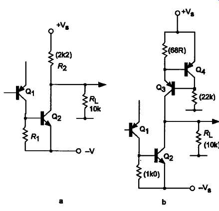
FIG. 14 Comparative amplifier circuits having different degrees of immunity
to hum or noise break-through from the DC supply lines.
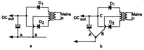
FIG. 15 Capacitor input power supply layouts.
A type of wiring layout which was commonly used in high quality amplifier systems, to avoid this and similar difficulties (before the widespread adoption of copper-clad printed circuit boards made this type of layout rather more difficult to implement), was that called 'single-point earthing', in which a common connection point was chosen as the 0V anchor point, and all of the 0V connections were taken directly to this. In the particular case of the circuit layout shown in FIG. 15a, trouble can be minimized if points A and B are the same connection, which is then joined to the 0V line, as shown in FIG. 15b. However, there will still be substantial current flows through the loop enclosing points A, B and C, and this will act as the single turn primary winding of an air-cored trans former, and will induce hum voltages in any wiring in the vicinity, as will any stray magnetic field from the mains transformer itself.
Modem practice, in high quality amplifier designs, favors the use of power supply transformers built around 'toroidal' cores, because the tight magnetic circuit of this type of core minimizes the transformer stray hum field. A practical point to keep in mind is that the magnitude of all such induced hum voltages will increase as the physical sizes of the primary (hum generating) and secondary (hum pick-up) loops are increased (because the larger loop area increases the degree of relative coupling of the primary and secondary of this unintended 'transformer') so that layout designs which ensure that all such conducting loops are as short as possible will help minimize the induced hum voltages. This is also important in respect of the AC mains hum field present in all buildings containing power service wiring, and in the case of very sensitive amplifier stages, the more compact the input/output signal loop can be made, in any signal stage, the lower the likelihood of hum pick-up.
Screening
A simple conducting screen will usually serve to pro vide electrostatic isolation from one circuit to another and minimize the unwanted effects of direct capacitative coupling. However, a plain metallic screen is relatively ineffective in reducing the extent of magnetic coupling, because such a conducting housing will act as a short-circuited single-turn secondary winding. This means that currents will be induced in this loop, in the presence of an external magnetic field, and these currents will themselves generate an external magnetic field -- and so on.
Much better results are obtainable if such a screen is made from a material of high magnetic permeability, such as 'MumetaT or 'Permalloy', or others of the kinds listed in Section 2, Table 2.4. This is standard practice for the screening cans of microphone transformers, which are likely to employ a large number of turns of wire on their secondary windings (leading to a high sensitivity to stray magnetic fields), and are also usually situated at the inputs of high-gain amplifier units.
Balanced cables
The avoidance of hum pick-up, due to the interaction of stray external magnetic fields with low-level long path length signal cables, has led to the use of twin 'balanced' feeder systems to interconnect, for example, sound studio microphone lines.
The basic system is illustrated in FIG. 16, in which a signal, symmetrically balanced in respect to the screening of the cable, is taken to a differential amplifier, which amplifies only the difference voltage between the two incoming lines. By this means, problems due to hum pick-up on the cables -- which will run in parallel, closely spaced paths, and will therefore have identical hum voltages induced in them -- will be cancelled.
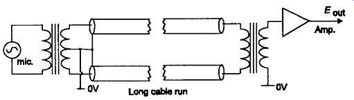
FIG. 16 Typical layout for balanced cable connections to minimize hum field
interference --- 0 V Long cable njn
Microphony
This is the name given to the irritating type of spurious circuit noise which occurs when the mechanical vibration of a sensitive component generates an unwanted electrical signal. This was a common problem with thermionic valves (tubes), where oscillatory motion of the grid windings, in relation to the cathode or anode of the valve, would lead to 'booming' or 'ringing' noises, but is seldom a source of trouble with semiconductor components, which are physically more robust and shock and vibration resistant. Care should be taken, however, in high gain amplifier systems, in the mounting of both components and PC boards, to limit the extent to which they can move in relation to one another.
A particular form of microphony is that which can arise in the screened cables used to interconnect very low signal level systems, particularly where there is a DC potential difference between the inner core and the outer screening braid. In this case, when the physical separation between these conductors is altered by flexure of the cable, or, perhaps, because it has been walked upon, the change in local cable capacitance will generate a noise voltage. Cables intended for use in this application, usually called 'microphone cables', employ an intermediate conductive screening layer, such as a coating of graphite or conductive plastic, bonded in intimate contact with the outer surface of the insulating core of the cable. Because this is at the 0V line potential, relative movement of the outer screening braid, in relation to this, won’t generate unwanted noise voltages.