AMAZON multi-meters discounts AMAZON oscilloscope discounts
(cont. from part 1)
7. CRYSTAL OSCILLATORS
Frequency stability is the most important feature of an oscillator. Frequency stability is the ability to provide a constant frequency output under varying load conditions. Frequency stability of the output signal can be improved by proper selection of the components used for the resonant feedback circuit including the amplifier but there is a limit to the stability that can be obtained from normal LC and RC tank circuits. Some of the factors that affect the frequency stability of an oscillator include temperature, variations in the load and changes in the power supply. For very high stability, a quartz crystal is generally used as the frequency-determining device to produce a typical type of oscillator circuit known as crystal oscillators.
The crystal oscillators are implemented using the piezo-electric effect. This is actually realised when a voltage source is applied to a small thin piece of crystal quartz. The quartz crystal begins to change shape. This piezo-electric effect is the property of a crystal by which an electrical charge produces a mechanical force by changing the shape of the crystal. In reverse sense, a mechanical force applied to the crystal produces an electrical charge. This piezo-electric effect produces mechanical vibrations or oscillations which are used to replace the LC tank circuit and can be seen in many different types of crystal substances with the most important of these for electronic circuits being the quartz minerals because of their superior mechanical strength.
The quartz crystal is a very small, thin piece or wafer of cut quartz with the two parallel surfaces metalized to make the electrical connections in a crystal oscillator. The physical size and thickness of a piece of quartz crystal is tightly controlled since it affects the final frequency of oscillations and is called the characteristic frequency of the crystal. Once cut and shaped, the crystal cannot be used at any other frequency. The crystal's characteristic or resonant frequency is inversely proportional to its physical thickness between the two metalized surfaces. A mechanically vibrating crystal can be represented by an equivalent electrical circuit consisting of low resistance, large inductance and small capacitance as shown in FIG. 14 .
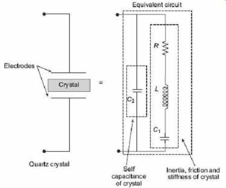
FIG. 14 Quartz crystal
Like an electrically tuned tank circuit, a quartz crystal has resonant frequency with very high Q factor due to low resistance. The frequencies of quartz crystals range from 4 kHz to 10 MHz. The cut of the crystal also determines how it will vibrate and behave as some crystals will vibrate at more than one frequency. Also, if the crystal is of varying thickness, it has two or more resonant frequencies having both a fundamental frequency and harmonics such as second or third harmonics. However, usually the fundamental frequency is more pronounced than the others and this is the one used. The equivalent circuit above consists of three reactive components and there are two resonant frequencies, the lowest is a series-type frequency and the highest a parallel-type resonant frequency.
In a crystal oscillator circuit, the oscillator will oscillate at the crystal's fundamental series resonant frequency as the crystal always intends to oscillate when a voltage source is applied to it. It is also possible to tune a crystal oscillator to any even harmonic of the fundamental frequencies, (2nd , 4th , 8th , etc.) and these are known generally as harmonic oscillators while overtone oscillators vibrate at odd multiples of the fundamental frequencies, (3rd , 5th , 11th , etc). Crystal oscillators that operate at overtone frequencies do so using their series resonant frequency.
7.1 Colpitts Crystal Oscillator
The design of a Colpitts crystal oscillator is very similar to the Colpitts oscillator. The LC tank in the Colpitt oscillator circuit has been replaced by a quartz crystal as shown below in FIG. 15 . The input signal to the base of the transistor is inverted at the transistors output. The output signal at the collector is then taken through 180° phase shifting network which contains the crystal operating in a series resonant mode.
The output is fed back to the input which is in-phase with the input providing the necessary positive feedback. Resistors R1 and R2 bias the transistor in class-A operation and the resistor R e is taken so that the loop gain is slightly higher than unity. Capacitors C 1 and C 2 are made as large as possible in order to get the frequency of series resonant mode of the crystal.
This frequency does not depend upon the values of these capacitors. The circuit diagram above of the Colpitts crystal oscillator circuit shows that capacitors C1 and C2 shunt the output of the transistor which reduces the feedback signal. Therefore, the gain of the transistor limits the maximum values of C1 and C2 . Another important point is that the output amplitude should be kept low in order to avoid excessive power dissipation in the crystal, otherwise, the crystal could destroy itself by excessive vibration.
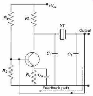
FIG. 15 Colpitts crystal oscillator
8. PIERCE OSCILLATOR
The Pierce oscillator is another common design of a crystal oscillator. It uses the crystal as part of its feedback path instead of the resonant tank circuit. A JFET is used as amplifier as it provides a very high input impedance with the crystal connected between the drain (output) terminal and the gate (input) terminal as shown in FIG. 16 .
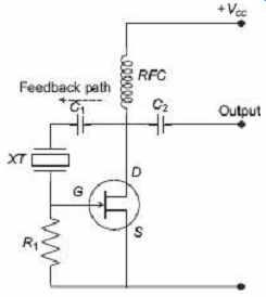
FIG. 16 Pierce crystal oscillator
In the above circuit, the crystal determines the frequency of oscillations and operates on its series resonant frequency giving a low-impedance path between output and input. It gives 180° phase shift at resonance and makes the feedback positive. The maximum voltage range at the drain terminal sets the amplitude of the output sine wave. Resistor R 1 regulates the amount of feedback and crystal drive. The voltage across the Radio Frequency Choke (RFC) reverses during each cycle. The Pierce oscillator can be implemented using the minimum number of components. Because of this, Pierce oscillators are used to design most digital clocks, watches and timers, etc.
9. MICROPROCESSOR CLOCKS
The crystal quartz oscillator is the most suitable frequency-determining device in virtually all microprocessors, microcontrollers, PICs and CPUs, used to generate their clock waveforms. Crystal oscillators provide the highest accuracy and frequency stability compared to resistor-capacitor or inductor-capacitor oscillators. The CPU clock dictates how fast the processor can process the data, and a microprocessor having a clock speed of 3 MHz means that it can process data internally 3 million times a second at every clock cycle. Generally, all that is needed to produce a microprocessor clock waveform is a crystal and two ceramic capacitors of values ranging between 15 to 33 pF as shown in FIG. 17 .
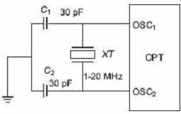
FIG. 17 Microprocessor oscillator
Most microprocessors, microcontrollers and PICs have two oscillator pins labeled OSC 1 and OSC 2 to connect to an external quartz crystal, RC network or even a ceramic resonator. In this application, the crystal oscillator produces a train of continuous squarewave pulses whose frequency is controlled by the crystal which in turn executes the instructions that control the device.
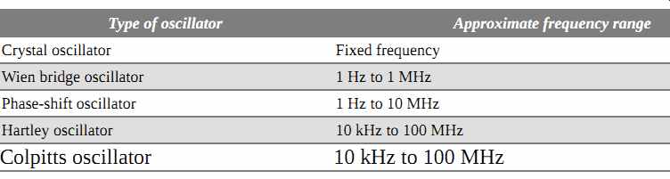
Table 1 Oscillators with their operating frequency
range
Type of oscillator Approximate frequency range
Crystal oscillator Fixed frequency Wien bridge oscillator 1 Hz to 1 MHz Phase-shift oscillator 1 Hz to 10 MHz Hartley oscillator 10 kHz to 100 MHz
Colpitts oscillator 10 kHz to 100 MHz
10. SQUARE WAVE AND PULSE GENERATORS
Wave shape, or wave profile, of a single pulse is shown in FIG. 18 . The characteristics of a single pulse are given below.
• The voltage rises very rapidly from zero to its maximum value.
• It stays steady at the maximum value for a time.
• It then falls very rapidly back to zero.
• The duration of a pulse can be anywhere from a very long time (days) to a very short time (picoseconds or less).
• Pulses do not rise and fall instantaneously but take time (which may be very short).
• They are called the rise and fall times.
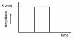
FIG. 18 Wave shape of a single-pulse
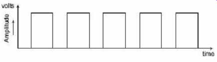
FIG. 19 Waveform of pulse train
As shown in FIG. 19 , a few characteristics of pulse trains are stated below:
• If pulses occur one after another, they are called a pulse train.
• The duration time of a pulse is called the mark.
• The time between pulses is called the space.
• The relative times are expressed as the mark-to-space ratio.
• Mark to space ratios may vary.
10.1 Typical Square Wave Generator
A continuous signal with regular wave shape is one requirement in a wide range of applications. One of the most important of these is a square-wave generator.
The circuit in FIG. 20 uses an op-amp as comparator with both positive and negative feedback to control its output voltage. Because the negative feedback path uses a capacitor while the positive feedback path does not, there is a time delay before the comparator is triggered to change state. As a result, the circuit oscillates, or keeps changing state back and forth at a predictable rate.
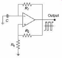
FIG. 20 Square wave generator circuit using
op-amp
Since no force or excitation is given to limit the output voltage, it will switch from one extreme to the other. If it is assumed that output voltage starts at −12 volts then the voltage at the positive or non-inverting input terminal will be set by R 2 and R 1 to a FIG. 20 … fixed voltage equal to −12 R 1 /( R 1 + R 2 ) volts. Now, it becomes the reference voltage for the comparator, and the output will remain unchanged until the negative or inverting input terminal becomes more negative than this value. But the inverting terminal is connected to a capacitor ( C ) which is gradually charging in a negative direction through the resistor R f .
Since C is charging towards −12 volts, but the reference voltage at the non-inverting input is necessarily smaller than the −12 volt limit, eventually the capacitor will charge to a voltage that exceeds the reference voltage. When that happens, the circuit will immediately change state. The output will become +12 volts and the reference voltage will abruptly become positive rather than negative. Now the capacitor will charge towards +12 volts, and the other half of the cycle will take place. The output frequency is given by the approximate equation:
In the practical field, the circuit-component values are chosen such that R 1 is approximately R f /3, and R 2 is in the range of 2 to 10 times R 1 .
10.2 OP-AMP Astable Multivibrator and Monostable Multivibrator Circuits
Relaxation oscillators are normally non-sinusoidal waveform generators. The relaxation oscillator using an op-amp shown in FIG. 21 is a square-wave generator. Square waves are relatively easy to generate.
The frequency of oscillation of a circuit is dependent on the charging and discharging of a capacitor C through the feedback resistor R f . The main component of the oscillator is an inverting op-amp working as comparator. A comparator circuit has positive feedback which increases the gain of the amplifier. A comparator circuit having positive feedback offers two advantages.
First, the high gain causes the op-amp's output to switch very quickly from one state to another and vice versa. Second, the use of positive feedback gives the hysteresis loop in the circuit operation.
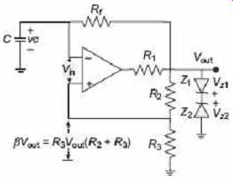
FIG. 21 Op-amp square-wave generator
As shown in FIG. 21 , in the op-amp square-wave generator, the output voltage V out is connected to ground through two Zener diodes Z1 and Z2 , connected back-to-back and is limited to either VZ2 or VZ1 . A fraction of the output is fed back to the non-inverting (+) input terminal. A combination of R f and C act as a low-pass RC circuit which is used to integrate the output voltage V out The capacitor voltage V c is applied to the inverting input terminal instead of external signal.
At that point of time, the differential input voltage is given as V in = V c − βV out .
When V in is + ve V out = − V zl
... and when V in is −ve , V out = + V z2 .
Consider an instant when V in < 0. At this instant, V out = + V z 2 , and the voltage at the non-inverting (+) input terminal is βV z2 , the capacitor C charges exponentially towards V z2 , with a time constant R f C. The output voltage remains constant at V z2 until v c equal ...
βV z2 . When it happens, comparator output reverses to − V z 1 . Now v c changes exponentially towards − V z 1 with the same time constant and again the output makes a transition from
− V z 1 to + V z 2 when V c equals −βV z1
Let V z 1 = V z 2
The time period, T of the output square wave is determined using the charging and discharging phenomena of the capacitor C . The voltage across the capacitor V c when it is charging from −B V z to + V z is given by
V c = [1 − (1 + β)]e −T/2τ
where τ = R f C
The waveforms of the capacitor voltage v c and output voltage V out (or v z ) are shown in FIG. 22.
When t = t /2,
V c = +βV z or + βV out
Therefore, βV z = V z [1 − (1 + β)e − T/2τ ] or e −T/2τ = (1 − β)/(1 + β ) or T = 2τ log e [(1 −β)/(1 + β)] = 2 R fc log e [1 + (2 R 3 / R 2 )]
FIG. 22 Output and capacitor voltage waveforms
Here, the frequency ( f = 1/ T ), of the square wave is independent of the output voltage V out . This circuit is also known as free-running or astable multivibrator. This circuit has two quasi-stable states as shown in FIG. 22 . The output remains in one state for the time T 1 and then a rapid transition to the second state and remains in that state for time T2 .
The cycle repeats itself after time T = ( T 1 + T 2 ). where, T is the time period of the squarewave.
The op-amp square-wave generator offers good performance in the frequency range of about 10 Hz − 10 kHz. But, at higher frequencies, the slew rate of the op-amp limits the slope of the output square wave. The matching of two Zener diodes Z 1 and Z 2 decides symmetry of the output waveform. The unsymmetrical square wave ( T 1 not equal to T 2 ) can be obtained by choosing different charging time constants for charging the capacitor C to + V out and − V out
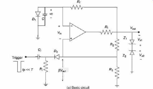
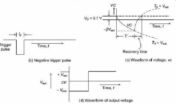
FIG. 23 Pulse generator/monostable circuit and
waveforms
A pulse generator circuit, as shown in FIG. 23 , is a monostable multivibrator A Monostable Multi Vibrator (MMV) has one stable state and one quasi-stable state. An external triggering pulse pushes the circuit to operate in the quasi-stable state from the stable state. The circuit comes back to its stable state after a time period T . As a result, a single output pulse is generated in response to an input pulse and is referred to as a one shot or mono shot. The monostable multivibrator circuit shown in FIG. 23 . is obtained by modifying the previous circuit by connecting a diode D 1 across the capacitor C so as to clamp v c at v d during positive excursion.
At steady state, the circuit will remain in its stable state and the output will be V OUT = + V OUT or + V z . The capacitor C is clamped at the voltage V D (= 0.7 V ). The voltage V D must be less than βV OUT for V in < 0. The circuit can be switched to the other state by applying a negative pulse with amplitude greater than βV OUT − V D to the non-inverting (+) terminal of the op-amp. If a trigger pulse with amplitude greater than βV OUT − V D is given,…
V in goes positive causing a transition in the state of the circuit to − V out . The capacitor C starts charging exponentially with a time constant of τ = R f C towards V OUT and diode D 1 becomes reverse-biased. When the capacitor voltage v c becomes more negative than − βV OUT , V in becomes negative and, therefore, the output swings back to + V OUT which is the steady-state output. The capacitor now charges towards + V OUT till v c attains V D and capacitor C becomes clamped at V D . The trigger pulse, capacitor voltage waveform and output voltage waveform are shown in FIG. 23(b), 23(c) and 23(d) respectively.
The trigger pulse width T must be much smaller than the duration of the output pulse generated, i.e. T P = T and for reliable, operation the circuit should not be triggered again before T.
During the quasi-stable state, the exponential profile of the capacitor voltage is expressed as, …
v c = − V OUT + ( V OUT + V D)e −t/τ
At, t = T , v c = − βV OUT
So − βV OUT = − V OUT + ( V OUT + v D ) e − T/τ
or, T = R f C log e (1 + V D / V out )/ 1 − β Normally, V D << V OUT and taking R 2 = R 3
The factor, β = R 3 /( R 2 + R 3 ) = 1/2 So, T = R f C log e 2 = 0.693 R f C
11. TRIANGULAR WAVE GENERATOR
Simply integrating the generated square wave can produce a triangular wave. With the basic squarewave-generator circuit, if a gradually charging capacitor is used to set the timing or frequency of the circuit then the desired triangular signal may be obtained. Since the capacitor is charging through a resistor, the charging profile necessarily follows a logarithmic curve, rather than a linear ramp.
As shown in FIG. 24 , in the right part of the circuit, a separate integrator is used to generate a ramp voltage from the generated square wave. As a result, both waveforms from a single circuit can be obtained. Note that the integrator inverts as well as integrating, so it will produce a negative-going ramp for a positive input voltage, and vice versa.
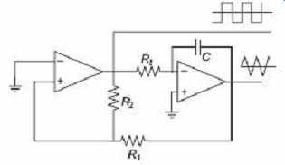
FIG. 24 Triangular wave generator
Since an op-amp is in use in the integrator, to get the triangle wave, a logarithmic response is not obtained anywhere in the circuit. As a result, the equation for the operating frequency is ...
The square-wave amplitude is still the limit of voltage transition, which are assuming here to be ±12 volts. The triangle wave's amplitude is set by the ratio of R 1 / R 2 .
The circuit shown in FIG. 25 is an example of a relaxation oscillator designed with two op-amps. The integrator output waveform will be triangular if the input to it is a square wave. So, a triangular-wave generator can be formed by simply cascading an integrator and a square-wave generator, as illustrated in FIG. 25(a). To implement the circuit, a dual op-amp, two capacitors, and at least five resistors are required. The rectangular-wave output swings between + V sat and − V sat with a time period determined.
The frequency of triangular-waveform and the square waveform are same.
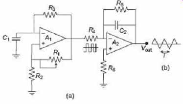
FIG. 25 Basic circuit of triangular-wave generator
The input to the integrator A 2 is a square wave and its output is a triangular waveform, the output of the integrator will be a triangular wave only when R 4 C 2 > T /2; where T is the time period of the square wave. As a general rule, R 4 C 2 should be equal to T . To obtain a stable triangular wave, it may also be necessary to shunt the capacitor C 2 with resistance R 5 = 10 R 4 and connect an offset volt compensating network at the non-inverting (+) input terminal of the op-amp A 2 . As usual, the frequency of the triangular-wave generator is limited by the op-amp slew rate. It is better to use a high slew rate op-amp (like LM 301), to generate triangular waveforms of relatively higher frequency.
With fewer components, another triangular-waveform generator can be formed and the circuit of that is shown in FIG. 26 (a). The arrangement consists of a Schmitt trigger in non-inverting configuration followed by an integrator. The rectangular wave output of the Schmitt trigger drives an integrator. The integrator generates a triangular wave, which is fed back and used to drive the Schmitt trigger. Thus, the first part of the circuit drives the second part of the circuit, and the second drives the first. But the question arises on how the circuit gets started at the outset. This part is explained as follows.
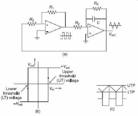
FIG. 26 (a) Feedback circuit with Schmitt trigger
and integrator producing triangular output waveform (b) Transfer characteristic
of Schmitt trigger (c) Output waveforms
The fact is that the moment the Schmitt trigger is connected to power supplies, the output of the Schmitt trigger must be either at low state or at high state. If the Schmitt trigger output is low then the output of the integrator will be a rising ramp and for Schmitt trigger of high output, the integrator will produce a falling ramp. In any case, the triangular waveform will start to generate, and the positive feedback to the Schmitt trigger input keeps it going. The transfer characteristic of the Schmitt trigger is shown in FIG. 26 (b). When the output is low, the input must increase to the upper threshold voltage to switch the output to high. Likewise, when the output is high, the input must fall to the lower threshold voltage to switch the output to low. The triangular wave produced by the integrator is capable of driving the Schmitt trigger. When the output of the Schmitt trigger is low, the integrator develops a rising ramp which increases till it reaches the upper threshold voltage, as illustrated in FIG. 26 (c). At this point, the output of the Schmitt trigger switches to the high state and forces the triangular wave to reverse in direction.
The negative or falling ramp produced by the integrator now falls till it reaches the upper threshold voltage, where another Schmitt output change occurs.
12. SINE WAVE GENERATOR
The demand of sine waves in many electronic applications is very high. The circuit, shown in FIG. 27 is the scheme to implement a mathematical relationship between the sine and cosine trigonometric functions. By integrating a sine wave, an inverted cosine wave is obtained. A cosine waveform is actually the same waveform as the sine wave but shifted 90° in phase. If that cosine wave is integrated and another 90° phase shift is achieved, it produces a negative sine wave. Of course, each op-amp integrator introduces an inversion as well, so the output of the first integrator is actually a non-inverted cosine wave. This is reversed again by the second integrator, so its output is still a negative sine wave. By inverting the negative sine wave, the original sine wave can be restored.
In this circuit, R 1 is adjusted to ensure that oscillations start and to help set the output amplitude. The Zener diodes serve to limit the output signal amplitude by limiting the gain of the cosine amplifier beyond the desired level. This prevents the circuit from amplifying the signal beyond its ±12 volt limits.
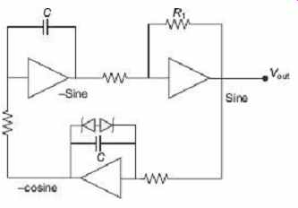
FIG. 27 A sine-wave generator circuit
The clipping effect caused by the Zener diodes does introduce some distortion, but with a reasonable setting of R 1 this effect is very slight, and the distortion it causes will be significantly reduced by the second integrator.
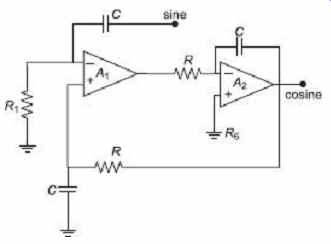
FIG. 28 A sine-wave oscillator
A classic oscillator circuit is shown in FIG. 28 . In this circuit, the op-amp offsets must be precisely balanced; otherwise, they will accumulate on the two integrators and gradually damp out the oscillations. This circuit can be implemented nicely using a dual op amp such as the 1458. All three capacitors are the same, and R t is taken very slightly less than R to ensure that the oscillations start the moment power is applied. Here, the frequency of oscillations is f = 1/2 RC . The frequency response of the op amps in use determines the maximum frequency of oscillations. In the circuit, the loop gain will decrease as frequency increases, and oscillations cannot be sustained if the loop gain is less than 1. The loop gain of this circuit must be greater than 1 to ensure oscillations. This circuit will also tend to clip the output waveforms. However, the same double-Zener clipping scheme in the circuit can be applied to the cosine integrator, to limit the signal amplitude and prevent either op amp from getting saturated.
As both sine and cosine waves are available, this circuit is also known as a quadrature oscillator.
13. FUNCTION GENERATORS
A function generator is a signal source that has the capability of producing different types of waveforms as its output signal. The most common output waveforms are sine waves, triangular waves square waves and sawtooth waves. The frequencies of such waveforms may be adjusted from a fraction of a hertz to several hundred kilohertz.
Actually, the function generators are very versatile instruments as they are capable of producing a wide variety of waveforms and frequencies. In fact, each of the waveforms they generate are particularly suitable for a different group of applications. The uses of sinusoidal outputs and square-wave outputs have already been described in the earlier Sections. The triangular-wave and sawtooth wave outputs of function generators are commonly used for those applications which need a signal that increases (or reduces) at a specific linear rate. They are also used in driving sweep oscillators in oscilloscopes and the X -axis of X-Y recorders.
Many function generators are also capable of generating two different waveforms simultaneously (from different output terminals, of course). This can be a useful feature when two generated signals are required for a particular application. For instance, by providing a square wave for linearity measurements in an audio-system, a simultaneous sawtooth output may be used to drive the horizontal deflection amplifier of an oscilloscope, providing a visual display of the measurement result. For another example, a triangular wave and a sine wave of equal frequencies can be produced simultaneously. If the zero crossings of both the waves are made to occur at the same time, a linearly varying waveform is available which can be started at the point of zero phase of a sine wave.
Another important feature of some function generators is their capability of phase locking to an external signal source. One function generator may be used to phase lock a second function generator, and the two output signals can be displaced in phase by an adjustable amount. In addition, one function generator may be phase locked to a harmonic of the sine wave of another function generator. By adjustment of the phase and the amplitude of the harmonics, almost any waveform may be produced by the summation of the fundamental frequency generated by one function generator and the harmonics generated by the other function generator. The function generator can also be phase locked to an accurate frequency standard, and all its output waveforms will have the same frequency, stability and accuracy as the standard.
The block diagram of a function generator is given in FIG. 29 . In this instrument, the frequency is controlled by varying the magnitude of current that drives the integrator.
This instrument provides different types of waveforms (such as sinusoidal, triangular and square waves) as its output signal with a frequency range of 0.01 Hz to 100 kHz.
The frequency-controlled voltage regulates two current supply sources. The current supply source 1 supplies constant current to the integrator whose output voltage rises linearly with time. An increase or decrease in the current increases or reduces the slope of the output voltage and thus, controls the frequency.
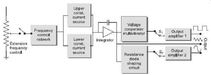
FIG. 29 Function generator block diagram
The voltage comparator multivibrator changes state at a predetermined maximum level, of the integrator output voltage. This change cuts off the current supply from the supply source 1 and switches to the supply source 2. The current supply source 2 supplies a reverse current to the integrator so that its output drops linearly with time. When the output attains a predetermined level, the voltage comparator again changes state and switches on to the current supply source. The output of the integrator is a triangular wave whose frequency depends on the current supplied by the constant-current supply sources.
The comparator output provides a square wave of the same frequency as the output. The resistance diode network changes the slope of the triangular wave as its amplitude changes and produces a sinusoidal wave with less than 1% distortion.
Voltage-controlled Oscillator
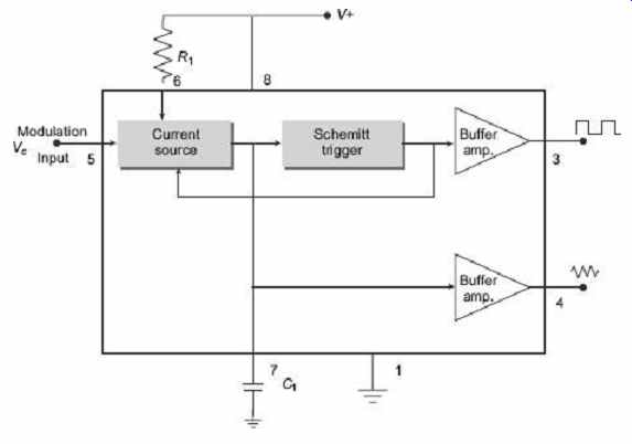
FIG. 30 block diagram of voltage-controlled
oscillator
In most cases, the frequency of an oscillator is determined by the time constant RC.
However, in cases or applications such as FM, tone generators, and Frequency-Shift Keying (FSK), the frequency is to be controlled by means of an input voltage, called the control voltage. This can be achieved in a Voltage-Controlled Oscillator (VCO). A VCO is a circuit that provides an oscillating output signal (typically of square wave or triangular waveform) whose frequency can be adjusted over a range by a dc voltage. An example of a VCO is the 566 IC unit as shown in FIG. 30 which provides simultaneously the square-wave and triangular-wave outputs as a function of input voltage. The frequency of oscillation is set by an external resistor R 1 and a capacitor C 1 and the voltage V c applied to the control terminals. FIG. 20 shows that the 566 IC unit contains current sources to charge and discharge an external capacitor C v at a rate set by an external resistor R 1 and the modulating dc input voltage. A Schmitt trigger circuit is employed to switch the current sources between charging and discharging the capacitor, and the triangular voltage produced across the capacitor and square wave from the Schmitt trigger are provided as outputs through buffer amplifiers. Both the output waveforms are buffered so that the output impedance of each is 50 f 2 . The typical magnitude of the triangular wave and the square wave are 2.4 V peak-to-peak and 5.4 V peak-to-peak.
The frequency of the output waveforms is approximated by
f out = 2( V + − V c )/ R 1 C 1 V +
14. RF SIGNAL GENERATOR
An RF oscillator is employed for generating a carrier waveform whose frequency can be adjusted typically from about 100 kHz to 30 MHz. Carrier wave frequency can be varied and indicated with the help of a range selector switch and a vernier dial setting. Range is selected by employing frequency dividers. Frequency stability of the oscillator is kept very high at all frequency ranges.
• The following measures are taken in order to achieve stable frequency output.
• Frequency of output voltage changes with the change in supply voltage so regulated power supply is used.
• Buffer amplifiers are used to isolate the oscillator circuit from output circuit so that any change in the circuit connected to the output does not affect the frequency and amplitude of the oscillator output.
• Temperature also causes change in oscillator frequency, so temperature-compensating devices are used.
• Q -factor of the LC circuit should be very high, say above 20,000. This can be achieved by employing quartz crystal oscillator in place of the LC oscillator.
• An audio-frequency modulating signal is generated in another very stable oscillator, called the modulation oscillator. Provision is made in the modulation oscillator for changing the frequency and the amplitude of the signal being generated.
In this oscillator, provision is also made to get various types of waveforms such as the square, triangular waves or pulses. The radio-frequency and the modulation-frequency signals are fed to a wide-band amplifier, called the output amplifier. Percentage of modulation can also be adjusted and it is indicated by the meter.
Modulation level can be adjusted up to 95% by a control device. The output of the amplifier is then fed to an attenuator and finally the signal goes to the output of signal generator. The output meter is provided to read the final output signal.
The accuracy to which the frequency of the RF oscillator is known is an important specification of the signal generator performance. Most laboratory-type models are usually calibrated to be within 0.5 − 1.0% of the dial setting. This accuracy is usually sufficient for most measurements. For greater accuracy, if needed, a crystal oscillator, whose frequency is known to be within 0.01% or better, may be used as an internal RF calibration source.
Another key specification of signal generators is their amplitude stability. It is very important that the amplitude of the output signal remains constant as the RF frequency is varied.