AMAZON multi-meters discounts AMAZON oscilloscope discounts
(cont. from part 1)
4. ANALOG INPUT SUBSYSTEM
Many data acquisition hardware devices contain one or more subsystems that convert (digitize) real-world sensor signals into numbers which computers can read. Such devices are called analog input subsystems (AI subsystems, A/D converters, or ADCs). Analog input subsystems convert real-world analog input signals from a sensor into bits that can be read by our computer. Perhaps the most important of all the subsystems commonly available, they are typically multichannel devices offering 12 or 16 bits of resolution.
4.1 Nyquist Criterion
Analog signals are continuous in time and in amplitude (within predefined limits).
Sampling takes a "snapshot" of the signal at discrete times, while quantization divides the voltage (or current) value into discrete amplitudes.
Sampling frequency has to be at least twice the frequency of the event that requires capture .
This rule is called the Nyquist Criterion . If one fails to follow this rule then a phenomenon called aliasing occurs. Aliasing is when a frequency higher than half of our sampling frequency gets "folded" back onto a frequency that is less than half of our sampling frequency. This creates a ghost signal that can really mess up our results.
4.2 A/D Conversion
A process of converting an analog signal into a digital signal comprises measuring the amplitude of the analog signal at consistent time intervals and producing a set of signals representing the measured digital value. The information in the digital signals and the known time interval enables one to convert the digital signal back to the analog signal.
Analog to digital conversion of a continuous input signal normally occurs in two steps:
sampling and quantization . The sampler takes a time-varying analog input signal and converts it to a fixed voltage, current, electrical charge, or other output level. The quantizer takes the constant sampled level and compares it to the closest level from a discrete range of values called quantization levels . The performance of analog and digital converters is typically quantified by two primary parameters, speed (in samples per second) and resolution (in bits). Higher resolution A/D converters typically require a large signal-to-noise ratio and good linearity. A/D converters with high sampling rates are frequently desired, but generally have lower resolution. There are two basic techniques for performing analog-to-digital conversion: an open-loop technique and a feedback technique.
4.3 Different Types of A/D Converters
While all analog-to-digital converters are classified by their resolution or number of bits, how the A/D circuitry achieves this resolution varies from device to device. There are four primary types of A/D converters used for industrial and laboratory applications:
Successive approximation Flash/Parallel Integrating Ramp/Counting Industrial and lab data acquisition tasks typically require 12 to 16 bits-12 are the most common. As a rule, increasing resolution results in higher costs and slower conversion speed.
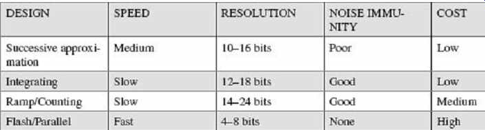
Table 3 Comparison of different A/D converters
1. Successive Approximation
A successive approximation ADC is a type of analog-to-digital converter that converts a continuous analog waveform into a discrete digital representation via a binary search through all possible quantization levels before finally converging upon a digital output for each conversion. It is the most common A/D converter design used for general industrial and laboratory applications ( Figure 13 ). This design provides an effective compromise among resolution, speed, and cost. An internal digital-to-analog (D/A) converter and a single comparator-essentially a circuit determines which of two voltages is higher-are used to narrow in on the unknown voltage by turning bits in the D/A converter on until the voltages match to within the least significant bit.
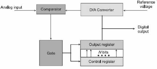
Figure 13 A/D conversion by successive approximation
2. Flash/Parallel
A flash A/D converter includes a reference voltage generator for generating a plurality of reference voltages, a first group of amplifiers having a plurality of amplifiers. Each of these amplifies a difference voltage between each reference voltage (generated by the reference voltage generator and a voltage of an input signal) and a second group of amplifiers having a plurality of amplifiers. It is used when higher speed operation is required. This design uses multiple comparators in parallel to process samples at more than 100 MHz with 8 to 12-bit resolution. Conversion is accomplished by a string of comparators with appropriate references operating in parallel (Figure 14 ).
The downside of this design is the large number of relatively expensive comparators that are required-for example; a 12-bit converter requires 4,095 comparators.
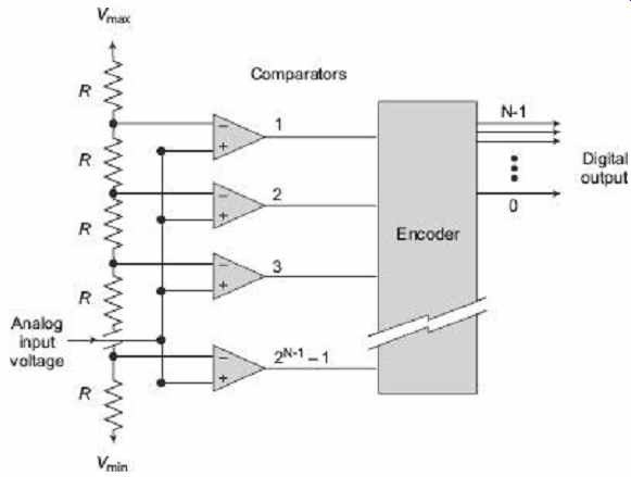
FIG. 14 A/D Conversion by Flash/Parallel technique
3. Integrating
Integrating analog-to-digital converters (ADCs) provide high resolution and can provide good line frequency and noise rejection. This type of A/D converter integrates an unknown input voltage for a specific period of time and then integrates it back down to zero. This time is compared to the amount of time taken to perform a similar integration on a known reference voltage. The relative times required and the known reference voltage then yields the unknown input voltage. Integrating converters with 12 to 18-bit resolution are available, at raw sampling rates of 10-500 kHz. These types of converters often include built-in drivers for LCD or LED displays and are found in many portable instrument applications, including digital panel meters and digital multimeters.
It also smoothes out signal noise because this type of design effectively averages the input voltage over time. And, if an integration period is chosen that is a multiple of the ac line frequency, excellent common-mode noise rejection is achieved. More accurate and more linear than successive approximation converters, integrating converters are a good choice for low-level voltage signals.
4. Ramp/Counter
The flash (simultaneous) A/D converter uses several voltage comparators that compare reference voltages with the analog input voltage. These converters use one comparator circuit and a D/A converter (Figure 15 ). This design progressively increments a digital counter and with each new count generates the corresponding analog voltage and compares it to the unknown input voltage. When agreement is indicated, the counter contains the digital equivalent of the unknown signal. The advantage of this circuit is that it provides a faster method of analog-to-digital conversion.
A variation on the counter method is the ramp method, which substitutes an operational amplifier or other analog ramping circuit for the D/A converter. This technique is somewhat faster.
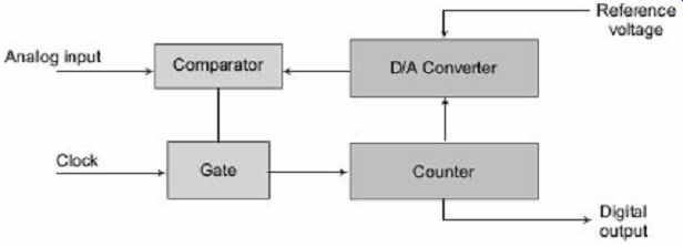
Fig. 15 A/D Conversion by counting/ramp technique
4.3 Performance
Performance of a ADC is judged by obtaining following parameters:
1. Resolution
Central to the performance of an A/D converter is its resolution, often expressed in bits.
An A/D converter essentially divides the analog input range into 2 N bits, where N is the number of bits. In other words, resolution is a measure of the number of levels used to represent the analog input range and determines the converter's sensitivity to a change in analog input. Amplification of the signal, or input gain, can be used to increase the apparent sensitivity if the signal's expected maximum range is less than the input range of the A/D converter. As higher resolution A/D converters cost more, it is especially important to not buy more resolution than one needs-if one has 1% accurate (1 in 100) temperature transducers, a 16-bit (1 in 65,536) A/D converter has probably more resolution than one needs.
2. Voltage Stability
Absolute accuracy of the A/D conversion is a function of the reference voltage stability (the known voltage to which the unknown voltage is compared) as well as the comparator performance. Overall, it is of limited use to know the accuracy of the A/D converter itself.
Accuracy of the system, together with the associated multiplexer, amplifier, and other circuitry is typically more meaningful.
3. Speed
The other primary A/D converter performance parameter that must be considered is speed throughput for a multi-channel device. Overall, system speed depends on the conversion time, acquisition time, transfer time, and the number of channels being served by the system.
4. Acquisition
Acquisition is the time needed by the front-end analog circuitry to acquire a signal. Also called aperture time , it is the time for which the converter must see the analog voltage in order to complete a conversion. Conversion is the time needed to produce a digital value corresponding to the analog value. Transfer is the time needed to send the digital value to the host computer's memory. Throughput, then, equals the number of channels being served divided by the time required to do all three functions.
Example 1 An analog to digital converter (ADC) measures voltages in the range of 0 to 25 V and has 12-bit accuracy. What is the smallest voltage step that the ADC can resolve?
Solution 12 bits = 2 12 = 4096 Therefore, the ADC can measure 4096 different values of voltage (from 0 to 4095 inclusive), the number of voltage steps is thus 4095 (one fewer than the number of different values available). Assuming that we set digital 0 to be equivalent to 0 V and digital 4095 to be equivalent to 25 V, each voltage step is simply given by 25 V/4095 = 0.006105 V = 6.105 mV
Example 2 Determine the number of output bits required for an ADC so that quantizing error less than 1 %.
Solution For 1 % quantizing error, count ≥ 100.
For n = 6, N = 2 6 - 1 = 63
For n = 7, N = 2 7 - 1 = 127
Example 3 A ramp-type ADC system uses a 10 MHz clock generator and a ramp voltage that increases from 0 V to 1.25 V in a time of 125 ms. Determine the number of clock pulses counted into the register when V = 0.9 V, and when it is 0.75 V.
Solution For V r = 1.25 V, t r = 125 ms
Example 4 If 3.45 V is applied to a 4-bit successive-approximation-type A/D converter which has a reference voltage of 5 V, what will be the digital output of the ADC?
Set d 3 = 1, Output 5/2 1 = 2.5 V.
Now, 3.45 > 2.5 and set d 3 = 1 Set d 2 = 1, Output = 2.5 + =3.75 Now, 3.45 < 3.75 and set d 2 = 0 Set d 1 = 1, Output = 2.5 + =3.125 Now, 3.125 < 3.45 and set d 1 = 1 Set d 0 = 1, Output = 3.125 + = 3.4375 Now, 3.4375 < 3.45 and set d 0 = 1.
Thus, the output of the A/D converter is 1011.
5. ANALOG OUTPUT SUBSYSTEM
Analog outputs commonly are used to operate final control elements in industrial environments like valves and motors. An analog output subsystem mainly consist of a Digital-to-Analog (D/A) converter, which is functionally opposite to an A/D converter.
Similar to analog input configurations, a common D/A converter often is shared among multiplexed output signals. Standard analog output ranges are often same as analog input standards: ±5 V dc, ±10 V dc, 0-10 V dc, and 4-20 mA dc, etc.
1. Key Specifications of an Analog Output Subsystem
(a) Settling Time Period required for a D/A converter to respond to a full-scale set point change.
(b) Linearity This refers to the device's ability to accurately divide the reference voltage into evenly sized increments.
(c) Range The reference voltage sets the limit on the output voltage achievable.
2. D/A Conversion
A digital-to-analog converter, or simply DAC, is a semiconductor device that is used to convert a digital code into an analog signal. Digital-to-analog conversion is the primary means by which digital equipment such as computer-based systems are able to translate digital data into real-world signals that are more understandable to or useable by humans, such as music, speech, pictures, video, and the like. It also allows digital control of machines, equipment, household appliances, and the like.
Essentially, the logic circuitry for an analog voltage output uses a digital word or series of bits, to drop in (or drop out, depending on whether the bit is 1 or 0) a series of resistors from a circuit driven by a reference voltage. This ladder of resistors can be made of either weighted-value resistors or an R-2R network using only two resistor values-one if placed in series ( Figure 16 ). While operation of the weighted-value network is more intuitively obvious, the R-2R scheme is more practical. Because only one resistor value need be used, it is easier to match the temperature coefficients of an R-2R ladder than a weighted network, resulting in more accurate outputs. Plus, for high resolution outputs, very high resistor values are needed in the weighted-resistor approach.
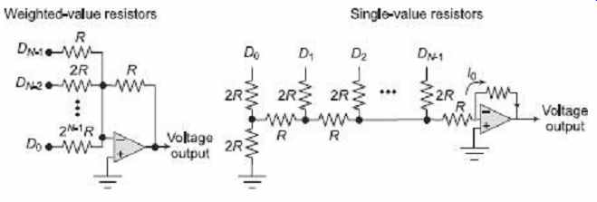
Figure 16 Weighted value and single-value resistor
networks for D/A conversion
By the Nyquist-Shannon sampling theorem, sampled data can be reconstructed perfectly provided that its bandwidth meets certain requirements (e.g., a base-band signal with bandwidth less than the Nyquist frequency). However, even with an ideal reconstruction filter, digital sampling introduces quantization error that makes perfect reconstruction practically impossible. Increasing the digital resolution (i.e., increasing the number of bits used in each sample) or introducing sampling dither can reduce this error.
5.1 Different Types of DACs
The most common types of electronic DACs are the following:
1. Pulse Width Modulator
It is the simplest DAC type. A stable current or voltage is switched into a low-pass analog filter with a duration determined by the digital input code. This technique is often used for electric motor speed control, and is now becoming common in high-fidelity audio.
2. Oversampling DACs or Interpolating DACs
They use a pulse density conversion technique. The oversampling technique allows for the use of a lower resolution DAC internally. A simple 1-bit DAC is often chosen because the oversampled result is inherently linear. The DAC is driven with a pulse density modulated signal, created with the use of a low-pass filter, step nonlinearity (the actual 1-bit DAC), and negative feedback loop, in a technique called delta-sigma modulation . This results in an effective high-pass filter acting on the quantization (signal processing) noise, thus steering this noise out of the low frequencies of interest into the high frequencies of little interest, which is called noise shaping (very high frequencies because of the over sampling). The quantization noise at these high frequencies are removed or greatly attenuated by use of an analog low-pass filter at the output (sometimes a simple RC lowpass circuit is sufficient). Most very-high-resolution DACs (greater than 16 bits) are of this type due to high linearity and low cost. Higher oversampling rates can relax the specifications of the output low-pass filter and enable further suppression of quantization noise. Speeds of greater than 100 thousand samples per second (for example, 192 kHz) and resolutions of 24 bits are attainable with Delta-Sigma DACs.
3. Binary Weighted DAC
It contains one resistor or current source for each bit of the DAC connected to a summing point. These precise voltages or currents sum to the correct output value. This is one of the fastest conversion methods but suffers from poor accuracy because of the high precision required for each individual voltage or current. Such high-precision resistors and current sources are expensive, so this type of converter is usually limited to 8-bit resolution or less.
4. R-2R Ladder DAC
It is a binary weighted DAC that uses a repeating cascaded structure of resistor values R and 2 R as shown in Figure 17 . This improves the precision due to the relative ease of producing equal-valued matched resistors (or current sources). However, wide converters perform slowly due to increasingly large RC -constants for each added R -2 R link.
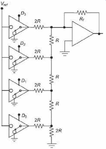
Figure 17 R-2R ladder DAC
5. Thermometer Coded DAC
It contains an equal resistor or current source segment for each possible value of DAC output. An 8-bit thermometer DAC would have 255 segments, and a 16-bit thermometer DAC would have 65,535 segments. This is perhaps the fastest and highest precision DAC architecture but at the expense of high cost. Conversion speeds of >1 billion samples per second have been reached with this type of DAC.
6. Hybrid DAC
It uses a combination of the above techniques in a single converter. Most DAC integrated circuits are of this type due to the difficulty of getting low cost, high speed and high precision in one device.
5.2 DAC Performance
DACs are at the beginning of the analog signal chain, which makes them very important to system performance. The most important characteristics of these devices are the following:
1. Resolution
This is the number of possible output levels the DAC is designed to reproduce. This is usually stated as the number of bits it uses, which is the base two logarithm of the number of levels. For instance, a 1 bit DAC is designed to reproduce 2 (2 1 ) levels while an 8 bit DAC is designed for 256 (2 8 ) levels. Resolution is related to the Effective Number of Bits (ENOB) which is a measurement of the actual resolution attained by the DAC.
2. Maximum Sampling Frequency
This is a measurement of the maximum speed at which the DACs circuitry can operate and still produce the correct output. As stated in the Nyquist-Shannon sampling theorem, a signal must be sampled at over twice the frequency of the desired signal. For instance, to reproduce signals in all the audible spectrum, which includes frequencies of up to 20 kHz, it is necessary to use DACs that operate at over 40 kHz. The CD standard samples audio at 44.1 kHz, thus, DACs of this frequency are often used. A common frequency in cheap computer sound cards is 48 kHz - many work at only this frequency, offering the use of other sample rates only through (often poor) internal resampling.
3. Monotonicity
This refers to the ability of DAC's analog output to increase with an increase in digital code or the converse. This characteristic is very important for DACs used as a low frequency signal source or as a digitally programmable trim element.
4. THD+N
This is a measurement of the distortion and noise introduced to the signal by the DAC. It is expressed as a percentage of the total power of unwanted harmonic distortion and noise that accompany the desired signal. This is a very important DAC characteristic for dynamic and small-signal DAC applications.
5. Dynamic Range
This is a measurement of the difference between the largest and smallest signals the DAC can reproduce expressed in decibels. This is usually related to DAC resolution and noise floor.
Example 5 Given a 3-bit DAC with a 1 V full-scale voltage and accuracy ±0.2%, find its resolution and accuracy in terms of voltage.
Example 6 An 8-bit D/A converter has +V ref = 5 V and -V ref = 0 V (Reference voltages). What is the output voltage when B in = 10110100? Find also V LSB .
Solution [...]
Example 7
A 6-bit D/A converter has a reference voltage of 10 V.
Calculate the minimum value of R such that the maximum value of output current does not exceed 10 mA. Find also the smallest quantized value of output current.
Solution
[...]
Example 8
A 6-bit D/A converter having 320 kW resistances is in LSB position. The converter is designed with weighted resistive network. The reference voltage is 10V. The output of the resistive network is connected to an OP-AMP with a feedback resistance of 5 kW. What is the output voltage for a binary input of 111.010?
Solution [...]
6. DIGITAL INPUT AND OUTPUT SUBSYSTEM
We saw that analog transducers sense continuous variables such as pressure and temperature and send the output in a continuous form to the ADC (analog to digital converter) via a signal conditioning device. In contrast to that, many transducers provide an output that is one of two states: high or low, open or closed, on or off, etc. For example, pressure might be too high or a temperature too low, triggering closure of a switch. This kind of input which is provided to the computer by the transducer is known as the digital input.
Outputs, too, are not always strictly analog. For example, solenoid valves typically are opened or closed; many pumps and heaters are simply turned on or off. The output of a printer is also purely digital in nature.
Digital I/O interfaces are commonly used in PC based DAQ systems to provide monitoring and control for industrial processes, generate patterns for testing in the laboratory and communicate with peripheral equipment such as data loggers and printers which have parallel digital I/O capabilities.
It is clear that these types of digital, or discrete, inputs and outputs (I/O) are much easier for microprocessor-based data acquisition systems to deal with than analog signals as the computer has a fully binary environment. Similar to analog-to-digital converters used for analog I/O, digital I/O is designed to deal directly with Transistor-to-Transistor Logic (TTL) level voltage changes. TTL typically sets the low-voltage level between 0 and 0.8 V and the high-voltage level between 2.0 and 5.0 V. Voltage levels between 0.8 and 2.0 V are not allowed. A voltage change, then, from the high range to the low range (or vice versa) represents a digital change of state from high to low, on to off, etc. and because acquiring an analog signal is more complex than acquiring a digital one, analog I/O channels also are more expensive. A clear comparison of the complexity in acquiring a signal in analog and digital forms is shown in Figure 18.
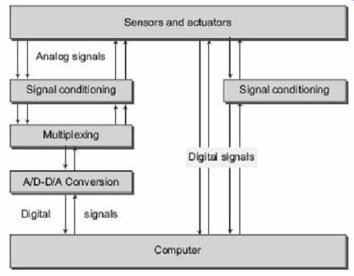
Figure 18 Comparison of digital and analog input
6.1 Digital Inputs
Many types of digital input signals from switch closures, relay contacts, or TTL compatible interfaces can be read directly by digital I/O cards ( Figure 18 ). Other types of inputs may require some signal-conditioning, most likely to reduce higher level voltage changes to TTL levels. A variety of signal-conditioning modules are available to provide isolation and other digital-conditioning functions. The most common type of digital input is the contact closure (Figure 19). Essentially, a sensor or switch of some type closes or opens a set of contacts in accordance with some process change. An applied electrical signal then determines whether the circuit is open or closed. Current flows if the circuit is closed, registering a "1" in a transistor at the computer interface. Conversely, an open circuit retains a high voltage (and no current), registering a "0" at the transistor.
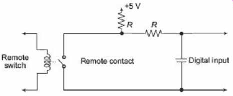
Figure 19 Contact type digital input
6.2 Digital Outputs
At its simplest, a digital output provides a means of turning something on or off.
Applications range from driving a relay to turning on an indicator lamp to transmitting data to another computer. For latching outputs, a "1" typically causes the associated switch or relay to latch, while a "0" causes the switch to unlatch. Devices can be turned on or off, depending on whether the external contacts are normally open or normally closed.
Standard TTL level signals can be used to drive 5 V relay coils; a protective diode is used to protect the digital output circuitry ( Figure 20 ). Because data acquisition boards can typically supply only 24 mA of driving current, they are intended primarily to drive other logic circuits, not final control elements. Scaling may be needed so that logical voltage levels are sufficient to cause switching in larger relays. Outputs intended to drive larger solenoids, contactors, motors, or alarms also may require a boost.
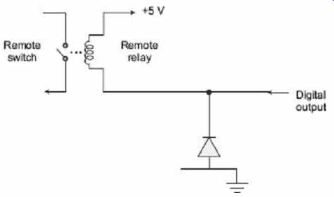
Figure 20 Contact type digital input
6.3 Counter/Timer and Pulse I/O
A somewhat separate class of digital I/O is pulse inputs and outputs, which typically is associated with frequency, counting or totalization applications. Pulse inputs might be used to count the rotations of a turbine flowmeter; pulse outputs might be used to drive a stepping motor.
Pulse inputs are handled in much the same way as digital logic inputs, but the output of the sensing circuit is normally connected to a counter rather than a specific bit position in the input register. Successive pulses increment or decrement the counter. Add an elapsed time measure and a frequency or pulse rate can readily be determined. Similar to an analog-to-digital converter, a counter is characterized by its number of bits-an N -bit counter can accumulate up to 2 N discrete events. Thus, a 16-bit counter can count to 2^16 = 65,536.
7. IEEE 488 INTERFACE
In 1965, Hewlett-Packard designed the Hewlett-Packard Interface Bus ( HP-IB ) to connect programmable instruments with computers. A high transfer rate around 1 Mbytes/second was possible to realize and due to this high transfer rate, this interface bus quickly gained popularity. It was later accepted as IEEE Standard 488-1975, and has evolved to ANSI/IEEE Standard 488.1-1987. Today, the name General Purpose Interface Bus (GPIB) is more widely used than HP-IB. ANSI/IEEE 488.2-1987 strengthened the original standard by defining precisely how controllers and instruments communicate.
Up to 15 devices can be connected in a single IEEE 488 bus by daisy-chaining. The speed is determined by the slowest device participating in the control and data-transfer handshakes. The GPIB bus is an 8-bit wide parallel interface system. The bus consists of 5 control lines, 3 handshake lines, 8 bi-directional data lines. It has a total of 24 lines, with the remaining lines occupied by ground wires. Additional features include TTL logic levels (negative true logic). It has the ability to communicate in a number of different language formats, and no minimum operational transfer limit. The maximum data-transfer rate is determined by a number of factors, often it is realised in 1 Mb/s.
Devices connected in the bus can be classified in the following category:
1. Controller
2. Talker
3. Listener
Figure 21 shows the connection of these three types of devices.
>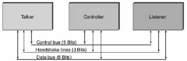
Figure 21 Connection diagram of different devices
with IEEE GPIB bus
A single device connected can have all the three or any two or at least any one of these features, but only one option will be active at a time. The first function of the bus controller (which is only one at a time) is to determine which device is active on the bus.
There may be many numbers of active listeners existing on the bus with an active talker as long as no more then 15 devices are connected to the bus. The controller sends interface messages over the bus to a particular active instrument. Each individual device is associated with a unique 5-bit BCD code (ID number). By using this code, the controller can coordinate the activities on the bus and the individual devices can be made to talk, listen (un-talk, unlisten) as determined by the controller.
1. Data Lines
The eight data lines, DIO1 through DIO8, carry both data and command messages. The state of the Attention (ATN) line determines whether the information is data or commands.
All commands and most data use the 7-bit ASCII or ISO code set, in which case the eighth bit, DIO8, is either unused or used for parity.
2. Handshake Lines
Three lines asynchronously control the transfer of message bytes between devices. The process is called a 3-wire interlocked handshake. It guarantees that message bytes on the data lines are sent and received without transmission error.
(a) NRFD (Not Ready For Data) This indicates when a device is ready or not ready to receive a message byte. The line is driven by all devices when receiving commands, by Listeners when receiving data messages, and by the Talker when enabling the HS488 protocol.
(b) NDAC (Not Data Accepted) This indicates when a device has or has not accepted a message byte. The line is driven by all devices when receiving commands, and by listeners when receiving data messages.
(c) DAV (Data Valid) This tells when the signals on the data lines are stable (valid) and can be accepted safely by devices. The Controller drives DAV when sending commands, and the Talker drives DAV when sending data messages.
3. Interface Management Lines
Five lines manage the flow of information across the interface:
(a) ATN (Attention) The Controller drives ATN true when it uses the data lines to send commands, and drives ATN false when a Talker can send data messages.
(b) IFC (Interface Clear) The System Controller drives the IFC line to initialize the bus and become CIC.
(c) REN (Remote Enable) The System Controller drives the REN line, which is used to place devices in remote or local program mode.
(d) SRQ (Service Request) Any device can drive the SRQ line to asynchronously request service from the Controller.
(e) EOI (End or Identify) The EOI line has two purposes-the Talker uses the EOI line to mark the end of a message string, and the Controller uses the EOI line to tell devices to identify their response in a parallel poll.
>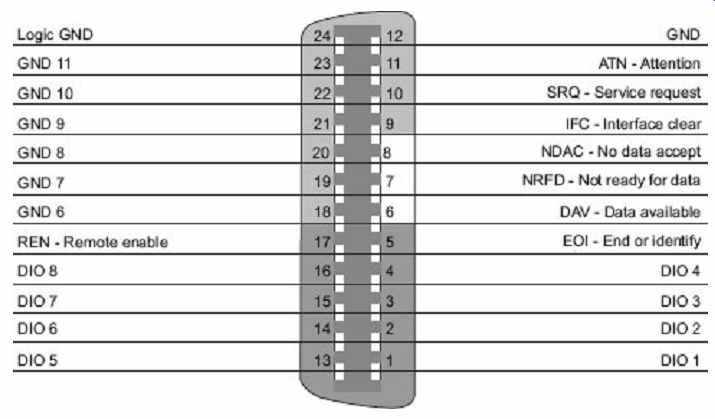
Figure 22 Pin-out description of GPIB bus
4. GPIB Data Transfer Operation
The three lines (DAV, NRFD and NDAC) are used to form three handshake lines which control the passage of data. The active talker controls the 'DAV' line (Data Valid) and the listener(s) control the 'NRFD' (Not Ready For Data), and the 'NDAC' (Not Data Accepted) line. In the steady state mode, the Talker hold 'DAV' high (no data available) while the listener hold 'NRFD' high (ready for data) and 'NDAC' low (no data accepted.
After the talker placed data on the bus it then takes 'DAV' low (data valid). The Listener(s) then send 'NRFD' low and send 'NDAC' high (data accepted). Before the Talker lifts the data off the bus, 'DAV' is taken high signifying that data is no longer valid.
If the 'ATN' line (attention) is high while this process occurs, the information is considered data but with the "ATN' line low, the information is regarded as an interface message. The other five lines on the bus ('ATN' included) are the bus-management lines.
These lines enable the Controller and other devices on the bus to enable, interrupt, flag, and halt the operation of the bus.
All lines in the GPIB are tri-state except for 'SQR', 'NRFD', and 'NDAC' which are open-collector. The standard bus termination is a 3K resistor connected to 5 volts in series with a 6.2K resistor to ground - all values having a 5% tolerance.
The standard also allows for identification of the devices on the bus. Each device should have a string of 1 or 2 letters placed somewhere on the body of the device (near or on the GPIB connector). These letters signify the capabilities of the device on the GPIB bus.
Table 4 Device capabilities on the GPIB bus
C Controller T Talker L Listener AH Acceptor Handshake SH Source Handshake DC Device Clear DT Device Trigger RL Remote Local PP Parallel Poll TE Talker Extended LE Listener Extended
Devices are connected together on the bus in a daisy-chained fashion. Normally, the GPIB connector (after being connected to the device with the male side) has a female interface so that another connector may be attached to it. This allows the devices to be daisy chained. Devices are connected together in either a linear or star fashion.
QUIZ
Objective-type Questions
1. The function of data acquisition system is (a) acquiring physical phenomena from the real world (b) sending signal to real world (c) processing and analyzing of signal (d) all of the above
2. Identify the element which is not part of a data acquisition system:
(a) Digital to analog converter (b) Filter (c) Display (d) Timer
3. Which A/D converter has highest conversion time?
(a) Flash type; (b) Dual slope integrating; (c) Successive approximation; (d) Ramp/Counting
4. How many devices can be connected in a single IEEE 488 bus? (a) 15 (b) 16 (c) 32 (d) Infinite
5. A signal has minimum and maximum values of -5 V and +5 V respectively. To record a 0.01 V change of the signal value, what bit length of A/D converter is required? (a) 4 bit (b) 8 bit (c) 10 bit (d) None of these
6. The function of notch filter is (a) pass high frequency signal (b) pass a particular band of signal (c) pass low frequency signal (d) none of these
7. If a signal has a bandwidth of 20 Hz to 20 kHz, what will be the minimum sampling frequency to acquire the signal so that the signal can be reproduced properly? (a) 20 Hz (b) > 20 Hz but < 20 kHz (c) < 20 kHz (d) > 20 kHz
8. The correct TTL logic levels are (a) 0-0.8 V and 2.0-5.0 V (b) 0-0.4 V and 2.4-5.0 V (c) 0 V and 5 V (d) 0-0.1 V and 4.9-5.0 V
9. An IEEE 488 bus contains (a) 8 data lines and 1a Address lines (b) 5 control lines, 3 handshake lines and 8 data lines (c) 3 control lines, 5 handshake lines and 8 data lines (d) 5 control lines, 3 hand shake lines, 8 data lines and 4 address lines
10. Which may not be the feature of a data acquisition application software? (a) Manage the data stored in computer memory (b) Plot acquired data (c) Report relevant information such as the number of samples acquired (d) Acquire data from real world
Short-answer Questions
1. Define a data acquisition system and draw the functional block diagram of a typical DAQ.
2. What are the different components of a DAQ? Briefly discuss those.
3. What are the different signal-conditioning units a data acquisition system contains? Briefly discuss those.
4. What are the different processes for isolation of field instrument from DAQ hardware?
5. State the different functions of driver software of a typical DAQ system.
6. Compare successive approximation, flash, integrating and ramp ADC.
7. Compare R - 2R DAC with a binary weighted DAC.
8. How are the digital input and output system connected with digital I/O pins of DAQ hardware?
9. How do the devices connected with IEEE 488 bus communicate with each other?
10. Write down the different functions of 5 control signals of IEEE 488 bus.
Long-answer Questions
1. An 8-bit ADC is converting a temperature signal which has a measuring range of 0 deg C to 800 deg C. Calculate the resolution of the temperature-measuring instrument.
2. Suppose a 10-bit ADC has + V ref and - V ref of +5 V and -5 V respectively. If the ADC is being used to convert a signal having minimum and maximum value of -1 V and +1 V then what amount of smallest voltage change can the ADC distinguish?
3. A ramp-type ADC system uses a 20 MHz clock generator and a ramp voltage that increases from 0 V to 5 V in a time of 0.5 sec. Determine the number of clock pulses counted into the register when V = 1 V, and when it is 2.5 V.
4. A 4-bit D/A converter has 320 kW resistances in LSB position. The converter is designed with weighted resistive network. The reference voltage is +5 V. The output of the resistive network is connected to an OP-AMP with a feedback resistance of 5 kW. What is the output voltage for a binary input of 101.110?
5. An 8-bit D/A converter has - V ref = -5 V and + V ref = +5 V respectively. Then calculate the output voltage when an
input of 140 10 (decimal) is given in the input of DAC. Also, find the V LSB .