AMAZON multi-meters discounts AMAZON oscilloscope discounts
1. History
With the static charging of transmission line cables, electronic systems have been vulnerable to the current pulse that comes from cable events.
Historically, cable discharge event (CDE) due to large computer system was a problem. In large mainframes, cables extended to the length of a room. When dragged on the floor, cables were charged due to triboelectric charging. When inserted into the ports of a large system, the cable would discharge into the port, leading to system failure. This was solved in early times by handling procedures of system operators to provide system level operation control. In these systems, "touch pads" were placed on the chassis of large systems, where the operator would discharge the cable during installation.
In the world today, the assembly, installation, and handling of cables are not a controlled process. This leads to the requirement of ESD solutions embedded in the systems, from the connectors, printed circuit boards (PCB), semiconductor components, and systems. With the growth of Ethernet networks, Ethernet interfaces require protection.
Ethernet network connections contain unshielded twisted pair (UTP). The telecommunication industry introduced registered jack (RJ) for connectors. An RJ is a standardized telecommunication network interface for connecting voice and data equipment.
Since 2000, it was clear that there was a need to develop a standard for CDE, leading to the document ESD Association. DSP 14.1--2003. ESD Association Standard Practice for the Protection of Electrostatic Discharge Sensitive Items--System Level Electrostatic Discharge Simulator Verification Standard Practice. Standard Practice (SP) document, 2003 [1].
In addition, there was a requirement to develop a measurement process for a cable, ESD Association. DSP 14.3--2006 ESD Association Standard Practice for the Protection of Electrostatic Discharge Sensitive Items--System Level Cable Discharge Measurements Standard Practice.
Standard Practice (SP) document, 2006 [2] as well as ESD Association, DSP 14.4--2007, ESD Association Standard Practice for the Protection of Electrostatic Discharge Sensitive Items--System Level Cable Discharge Test Standard Practice. Standard Practice (SP) document, 2007 (FIG. 1) [3].
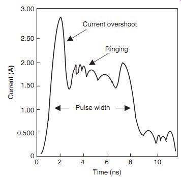
FIG. 1 Cable discharge event (CDE)
2. Scope
The scope of the CDE electrostatic discharge (ESD) test is for the testing, evaluation, and classification of cables. The test is to quantify the sensitivity or susceptibility of these components or systems to damage or degradation to the defined CDE test [1-3].
3. Purpose
The purpose of the CDE ESD test is for the establishment of a test methodology to evaluate the repeatability and reproducibility of systems to a defined cable discharge pulse event in order to classify or compare ESD sensitivity levels of systems [1-3].
4. Cable Discharge Event--Charging, Discharging, and Pulse Waveform
CDEs can impact the cable, the connector termination, the PCB, and internal components [4-12]. For example, a UTP CDE can discharge a large current due to its low source impedance. Other ESD models, such as human body model (HBM), machine model (MM), and charged device model (CDM), have high impedance. As a result, the charge from a cable discharge can be significant. In many cases, a CDE can exceed the latchup robustness of the components that are mounted on the PCB [13, 14].
4.1 Charging Process
The charging process of a cable can occur from two sources. A common source of charging is triboelectric charging between the cable and a ground surface. Triboelectric charge transfer can occur due to physical contact between the cable and flooring, conduits, or adjacent cables.
As an example, a Category 5 (CAT5) UTP cable can be placed on a floor or ground surface (FIG. 2(a)). FIG. 2 shows an example of only one pair of connectors. Dragging the cable across the floor can lead to charge transfer leading to charge accumulation on the cable when the cable is unterminated. The amount of charge transfer is dependent on the two materials in the triboelectric charge transfer process, cable characteristics, and the length of the cable. The charge will remain in the cable until leakage occurs, or termination. CAT5 and CAT6 UTP cables have low dielectric leakage characteristics, leading to storage of the charge along time. Environmental conditions (e.g., relative humidity) can also influence the storage time of the accumulated charge [6].
A second source of charging is electromagnetic induction. Electromagnetic induction can charge the cable without physical contact or triboelectric effect.
4.2 Discharging Process
To demonstrate the CDE, a telecommunication system is used as an example where the circuit is a media-dependent interface (MDI) transceiver. FIG. 2(b) shows the CAT5 cable and its associated ground plane. The UTP connections are attached to the registered jack 45 (RJ45) connectors. An isolation transformer is connected on the chassis side. The input of the isolation transformer is connected to a Bob Smith termination network [19]. The CDE can follow many paths in the network leading to a failure in the system [6].
4.3 Pulse Waveform
A CDE forms a square pulse waveform. FIG. 2(c) provides an example of a typical CDE.
The cable event typically has a fast rise time and an overshoot at the beginning of the event.
The waveform settles to a plateau. The plateau of the waveform has some structure associated with ringing. The length of the pulse event is a function of the length of the cable. The current magnitude is associated with the accumulated charge in the cable [1].
4.4 Comparison of CDE and IEC 61000-4-2 Pulse Waveform
The CDE and the IEC 61000-4-2 test are used on systems in the automobile industry. Comparing the cable discharge model to the IEC 61000-4-2, the CDE waveform and the IEC 61000-4-2 both pulses contain a fast event at the onset of the pulse. But the IEC 61000-4-2 exhibits an HBM-like waveform with a higher series impedance [13].
FIG. 2 (a) Charging process on Category 5 (CAT 5) cable. (b) Cable discharge event (CDE) discharging process and example test setup. (c) Cable discharge event (CDE) model pulse waveform
5. Equivalent Circuit
An equivalent circuit can be defined that represents the CDE forms a square pulse waveform. The CDE can be represented as an inductor-capacitor transmission line (FIG. 3(a)). The incremental model has an inductor per unit length between the input and the output of the cable. The incremental model of the cable is also represented by a capacitance per unit length.
As an individual circuit element, this can be represented as a transmission line symbol.
The CDE can be represented as an inductor-resistor-capacitor transmission line (FIG. 3(b)). The incremental model has an inductor and a series resistor per unit length between the input and the output of the cable. The incremental model of the cable also is represented by a capacitance per unit length. As an individual circuit element, this can be represented as a lossy transmission line symbol. In these test systems, the losses associated with the resistance per unit length is low.
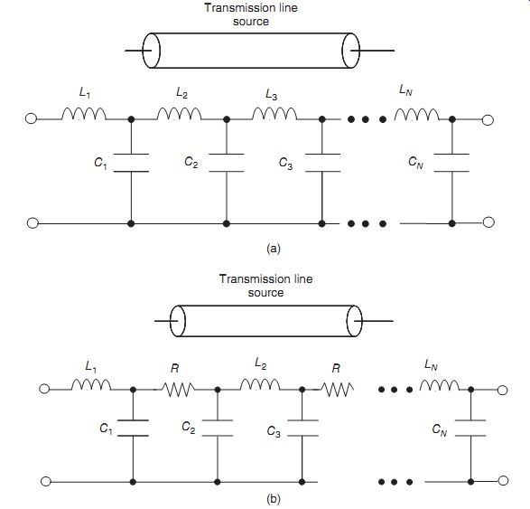
FIG. 3 (a) Cable discharge event (CDE) equivalent circuit model as
a lossless transmission line. (b) Cable discharge event (CDE) equivalent
circuit with parasitics as a lossy transmission line
6. Test Equipment
Commercial test systems exist for CDE evaluation. Commercial test systems were developed for standardization of the cable discharge test. These are discussed in the following sections.
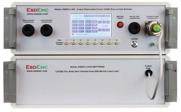
FIG. 4 Cable discharge event (CDE) commercial test system--ESDEMC ES631--LAN
cable discharge event (CDE) evaluation system (Reproduced with permission
of ESDEMC Technology LLC)
6.1 Commercial Test Systems
Commercial test systems exist for CDE evaluation such as the ESDEMC Corporation test system. The ESDEMC Model ES631-LAN CDE Evaluation System is shown in FIG. 4 [21]. The ES631-LAN CDE Evaluation System is a comprehensive test system designed to simulate the effects of charged Ethernet cable discharge to any Ethernet-based network system or device. The system allows for charging of the Ethernet cable to 4 kV, or differentially 2 kV.
The system includes embedded ESD current probes for discharging lines. The ES-631 system allows for four different test modes [21]:
• Single line discharge mode
• Differential pair discharge mode
• Contact sequence discharge mode
• "Through traffic" running mode.
This system allows the operator to be able to set up and analyze the CDE in different combinations. It also provides a "traffic" mode to evaluate through the CDE system itself. The test system allows for evaluation of different applications [21]:
• Ethernet CDE and analysis
• PHY ESD protection test and analysis
• Network switch/router ESD robustness test and analysis
• Automatic test equipment (ATE) for Ethernet system ESD
7. Test Measurement
For the CDE, the test equipment, sequence, and procedures are important for the measurement process. These are discussed in the following sections.
7.1 Measurement
For the CDE, the test equipment is important for the measurement process. FIG. 5(a) shows an example of a pulse generator serving as the cable source. The pulse generator has different pulse lengths for testing. In addition, the test system requires a fast pulse head module and an attenuator. FIG. 5(b) shows the target and target adapter [2].
For the CDE, measurement of the cable characteristics is important to the evaluation of the impact to the device under test (DUT). For the CDE, measurement of the cable characteristics is important to the evaluation of the impact to the DUT.
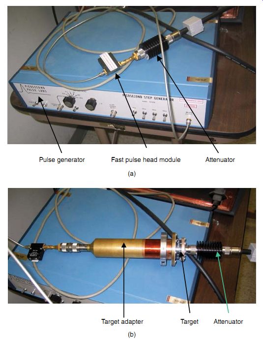
FIG. 5 (a) Test equipment. (b) Test equipment target and adapter.
7.2 Measurement -Transmission Line Test Generators
For the CDE, transmission line test generators exist for different impedance levels.
7.2.1 High-Impedance Transmission Line Test Generator
FIG. 6 shows an example of a high-impedance transmission line test generator. In the figure, a transmission line of length L is shown. The far end of the transmission line is unterminated. The outer conductor of the transmission line is grounded. A high-voltage charging source is connected to the transmission line through a switch and a high-impedance resistor element. The resistor element is 10MO. During the charging process, the switch is closed to allow charging of the transmission line cable. After the completion of the charging, the trans mission line is decoupled from the charging source. The transmission line is then discharged to the DUT through the switch and resistor network. The series resistor element is 300O.The resistor element to ground is 58-60O [2].
7.2.2 Low-Impedance Transmission Line Test Generator
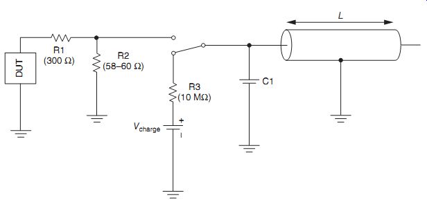
FIG. 6 Cable discharge event (CDE) measurement--high-impedance test
generator
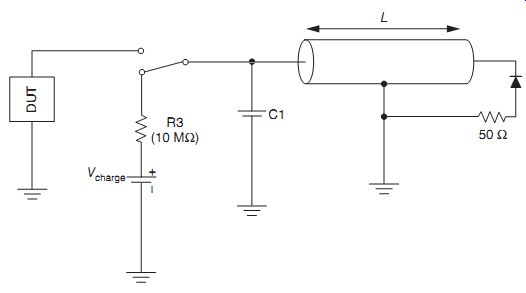
FIG. 7 Cable discharge event (CDE) measurement--low-impedance test
generator
FIG. 7 shows an example of a low-impedance transmission line test generator. In the figure, a transmission line of length L is shown. The far end of the transmission line is terminated using a 50O resistor and diode element to ground. The outer conductor of the transmission line is grounded. A high-voltage charging source is connected to the transmission line through a switch and a high-impedance resistor element. The resistor element is 10 M-O.
During the charging process, the switch is closed to allow charging of the transmission line cable. After the completion of the charging, the transmission line is decoupled from the charging source. The transmission line is then discharged to the DUT through the switch [1-3].
7.3 Measurement--Low-Impedance Transmission Line Waveform
An example of a waveform shows the characteristics of the CDE. FIG. 8(a) is a waveform from the low-impedance transmission line tester. The characteristics of the waveform involve a fast rise time, overshoot, and oscillation at the beginning of the pulse event. The waveform is followed by a voltage plateau until the end of the pulse event [1-3].
7.4 Schematic Capturing System Response to Reference Waveform
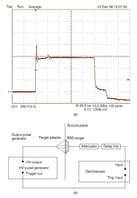
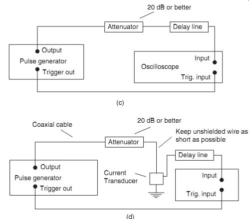
FIG. 8 (a) Low-impedance transmission line waveform. (b) Capturing
system response to reference waveform. (c) Capturing system response--alternate
current transducer. (d) Capturing system response--alternate current transducer
FIG. 8 (continued)
In the test system, to obtain highly accurate understanding of the system response, an ESD target and target adapter is key to the measurement system. FIG. 8(b) shows a high-level schematic for capturing the system response to the reference waveform. In this case, a high voltage pulse generator is used to establish an output pulse. A high-quality target adapter is connected to the high voltage pulse generator output. The ESD target is connected to a ground plane. The input of the target adapter is connected to an attenuator and a delay line. The delay line is connected to the input of a high-speed oscilloscope. The output trigger of the high voltage pulse generator is coupled to the oscilloscope trigger input [1-3].
In the test system, an alternate current transducer method is used to capturing the reference waveform. FIG. 8(c) shows a high-level schematic for capturing the system response to the reference waveform. In this case, a high voltage pulse generator is used to establish an output pulse. The pulse generator is connected to an attenuator and a delay line. The delay line is connected to the input of a high-speed oscilloscope. The output trigger of the high voltage pulse generator is coupled to the oscilloscope trigger input.
FIG. 8(d) shows a high-level schematic for capturing the system response to the reference waveform where a current transducer is added to the network. A coaxial cable is introduced between the pulse generator and attenuator. The pulse generator is connected to an attenuator and a delay line. The delay line is connected to the input of a high-speed oscilloscope. The output trigger of the high voltage pulse generator is coupled to the oscilloscope trigger input. It is recommended that the unshielded wire between the attenuator and current transducer is made as short as possible.
7.5 Tapered Transmission Lines
For standards development, it is important to provide the highest quality of understanding possible. To obtain high-quality measurements of the CDE, sophisticated measurement equipment is used to define a 50-O transmission line. High-quality transmission lines and targets are specifically designed in fine details. FIG. 9(a) shows an example of a constant impedance tapered transmission line adapter. FIG. 9(b) shows a cross-sectional view of the tapered transmission line. In the design, the angles of the transmission line are specified. The location of the mechanical tapered are also specified at the two ends of the transmission line.
FIG. 9(c) shows a commercial 50O transmission line target adapter (developed by the Barth Electronics Corporation) [30, 31].
7.6 ESD Current Sensor
For standards development, it is important to provide the highest quality of understanding possible in the design of the ESD current sensor. To obtain high-quality measurements of the CDE, the ESD current sensor construction has highly specified dimensions. FIG. 10(a) shows the ESD current sensor physical dimensions of top view, bottom view, and cross section [1-3].
FIG. 10(b) shows the construction elements of the ESD current sensor. This includes the SMA connector, the central brass part, the PTFE part I, SMD-resistor element, cover, top part of center conductor, and the PTFE part IFI. The diagram shows the placement and screw connections for assembly of the ESD current sensor [1-3].
FIG. 10(c) shows cross-sectional views of the construction elements of the ESD current sensor in finer details. This includes the PTFE-part I, PTFE-part IFI, SMA connector, the center conductor, cover, top part of center conductor, and the SMA connector [1-3].
8. Test Procedure
FIG. 11(a) shows the CDE test procedure. In the test procedure, the switch to the DUT must be opened prior to charging the cable. The switch between the high-voltage charging source and the cable is closed. The cable is then charged to a specified voltage level. The charged cable switch is then changed to apply the CDE to the DUT. The channels of the DUT are then evaluated. Depending on the failure criteria, the test is repeated and testing is continued to a higher voltage level.
In test systems for differential inputs, the test procedure can include introduction of different delays to the differential inputs using a delay control network.
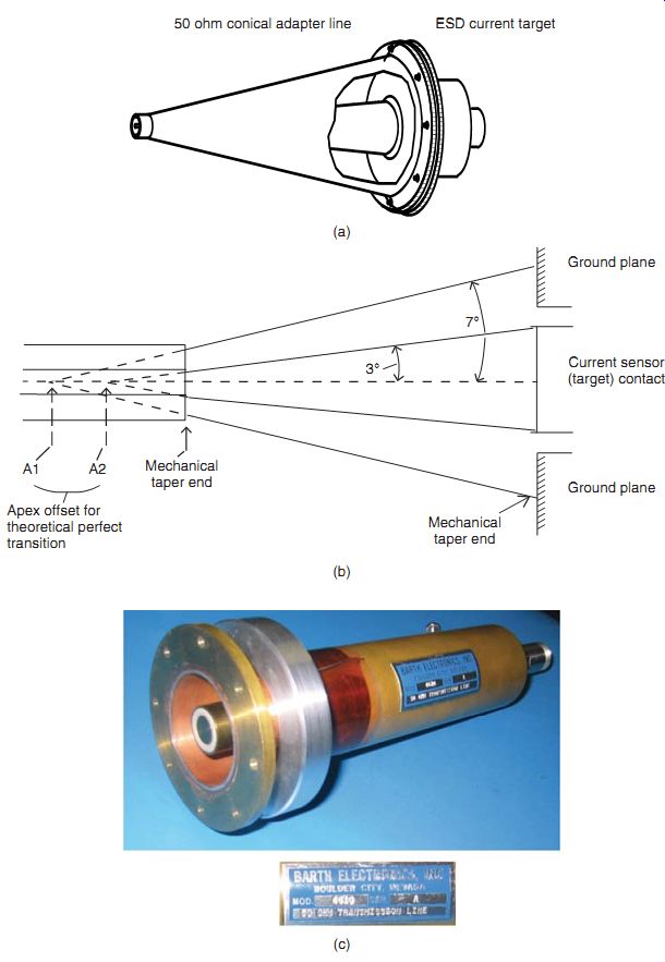
FIG. 9
(a) Constant impedance tapered transmission line. (b) Constant impedance
tapered trans mission line. (c) Tapered transmission line (Barth Electronics
Corp.)
9. Measurement of a Cable in Different Conditions
Measurement of a cable discharge is also a function of the test configuration and conditions.
In the following section, the test configuration, the conditions, procedure, and sequence are discussed [30, 34].
9.1 Test System Configuration and Diagram
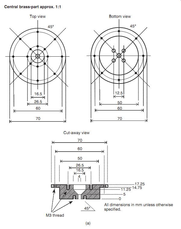
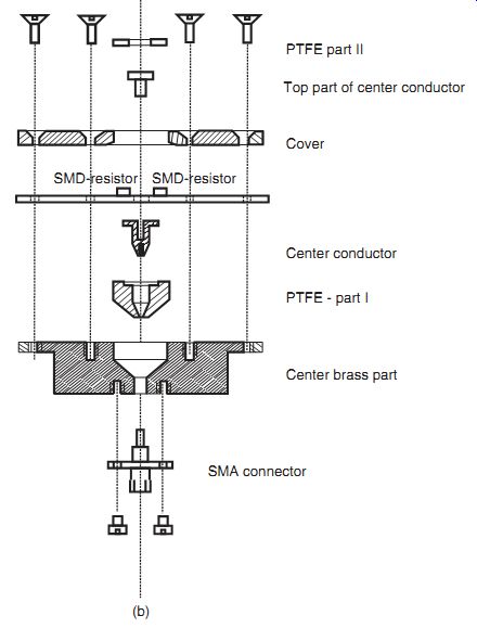
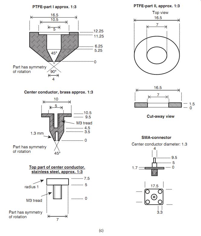
FIG. 10 (a) ESD current sensor. (b) ESD current sensor. (c) ESD current
sensor (ESD Association)
FIG. 11(b) shows a test configuration and diagram. The diagram addresses a key issue in cable measurement [30, 34]:
• Floor configuration
• Floor material
• Ground plane configuration
• Cable type (e.g., UTP, CAT4, CAT5)
• Length of the cable
• Configuration of the cable (held, coiled, etc.)
• Cable-to-ground plane conditions
• Target.
The figure shows an example of a cable test configuration. A vertical ground plane and horizontal floor is shown. A 100m cable is placed on the linoleum tile flooring. The first meter of the cable is raised near the vertical wall. An insulator is used to hold the cable and place the end of the cable near the target. An oscilloscope is connected to the target.
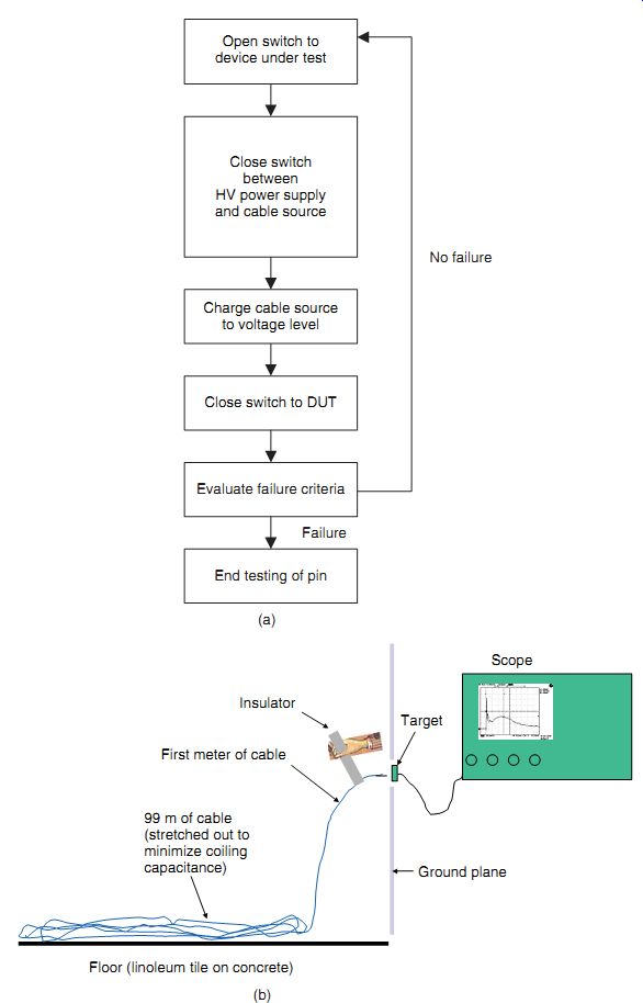
FIG. 11 (a) Cable discharge event (CDE) measurement--test procedure.
(b) Cable discharge test configuration (Reproduced with permission from ESD
Association)
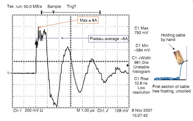
FIG. 12
Cable discharge event (CDE)measurement--holding cable ( ESD Association)
9.2 Cable Configurations--Handheld Cable
The cable signal response is altered by the configuration. In this section, the pulse event from a handheld cable is shown. The first section of the cable is free floating and uncoiled (FIG. 12). The pulse waveform is shown as well. A vertical ground plane and horizontal floor is shown. A 100m cable is placed on the linoleum tile flooring. The first meter of the cable is raised near the vertical wall. No insulator is used to hold the cable and place the end of the cable near the target. An oscilloscope is connected to the target [34].
9.3 Cable Configuration--Taped to Ground Plane
In this section, the cable is taped to the vertical ground plane. The first section of the cable is taped to the ground plane, and the rest of the cable is coiled (FIG. 13(a)). An insulator is used to hold the cable and place the end of the cable near the target. An oscilloscope is connected to the target. A peak current of 11.8A is shown [30, 34].
FIG. 13(b) shows a comparison of the cable discharge of a taped versus floating cable. The cable discharge of the initial peak current for the case of the cable taped to the wall is larger than the floating cable.
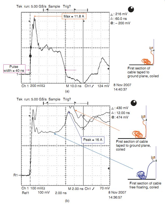
FIG. 13
(a) Cable discharge event (CDE) measurement--taped to vertical wall. (b)
Cable discharge event (CDE) measurement--taped to vertical wall versus floating
cable (ESD Association)
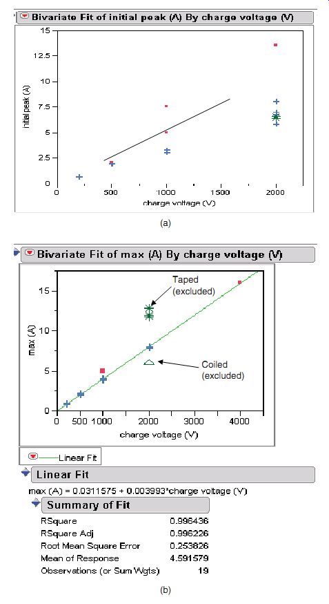
FIG. 14 (a) Cable discharge event (CDE) measurement--pulse analysis
summary. (b) Cable discharge event (CDE) measurement--pulse analysis summary--initial
peak current. (c) Cable discharge event (CDE) measurement--pulse analysis
summary--plateau current ( ESD Association)
9.4 Cable Configurations--Pulse Analysis Summary
The initial peak current can be shown related to the initial charging voltage. FIG. 14(a) shows the correlation between the peak current and the charging voltage.
FIG. 14(b) shows the bivariate it of the current versus the charging voltage. In the analysis, the case of the taped and coiled configurations is excluded from the correlation study.
The simplification of the it shows the initial peak current is equal to 0.004 times the charging voltage [34].
FIG. 14(c) shows the bivariate it of the plateau current versus the charging voltage. In the analysis, the case of the taped and coiled configurations is excluded from the correlation study. The simplification of the it shows the plateau current is equal to 0.003 times the charging voltage.
10. Transient Field Measurements
During a CDE, there is both the current from the discharge and associated electromagnetic transient fields. For short-length CDEs, test configurations can be established to evaluate the transient fields [34].
10.1 Transient Field Measurement of Short-Length Cable Discharge Events
FIG. 15(a) shows the test configuration and experimental setup for the discharge cur rent. A 1.0m-long cable is placed in a vertical configuration. The center conductor discharges through a switch to a 100-mm 50-O microstrip line that is terminated by a 50-Ohm resistor. A Tektronix CT-6 current probe measures the current discharge and records it on an oscilloscope. A 20 dB attenuator is used at the input to the oscilloscope [34].
FIG. 15(b) shows the test configuration and experimental setup for measurement of the magnetic field induced by the discharge current. A 1.0m-long cable is placed in a vertical configuration. The center conductor discharges through a switch to ground. The cable is placed 100mm from the H-field sensor. A 50-O resistor is placed on a 10-mm loop H-field sensor (FIG. 15(c)). The current loop is placed 100mm from the ground plane. A Tektronix CT-6 current probe measures the current in the loop sensor and records it on an oscilloscope. A 20 dB attenuator is used at the input to the oscilloscope [34].
FIG. 15(d) shows the test configuration and experimental setup for measurement of the electric field induced by the discharge current. A 1.0m-long cable is placed in a vertical configuration. The center conductor discharges through a switch to ground. The cable is placed 100mm from the E-field sensor. The E-field sensor is a short monopole antenna. The short monopole antenna loop is placed 100mm from the ground plane. The short monopole antenna loop is directly connected to the input of the oscilloscope. Examples of the monopole antenna loops are shown in FIG. 15(e) [33].
10.2 Antenna-Induced Voltages
Antenna-induced voltages are generated from the CDE [34]. FIG. 16 is an example of an antenna-induced voltage on the short monopole antenna detector. An oscillatory waveform is evident on the antenna detector. A peak-to-peak voltage of 2.3V occurs on the 10mm antenna at a 100mmspacing between the detector and the discharge cable in a nanosecond time regime.
Note that this voltage is significant enough to lead to failures in magnetic recording technology, as well as advanced CMOS technology.
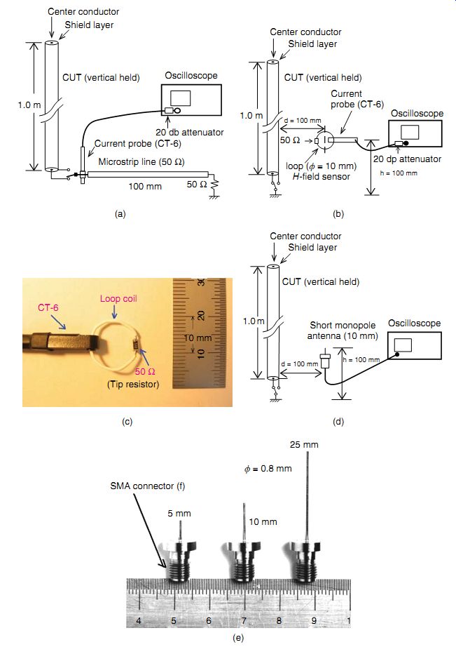
FIG. 15 (a) Transient discharge--discharge current. (b) Transient discharge--magnetic
field. (c) Magnetic current loop. (d) Transient discharge--electric field.
(e)Monopole antenna loops (Reproduced with permission from ESD Association)
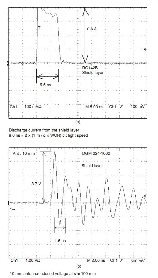
FIG. 16
Antenna-induced voltage (ESD Association)
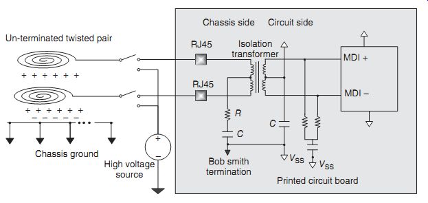
FIG. 17 Telecommunication CDE test system
11. Telecommunication Cable Discharge Test System
To demonstrate the CDE, a test system is needed to evaluate CDEs in a telecommunication system. As discussed, a telecommunication system includes CAT5 cables, a registered jack 45 (RJ45) connectors, an isolation transformer, a Bob Smith termination, and an MDI transceiver circuit (FIG. 17). In the test system, a high-voltage charging source, relays, and switches are needed to simulate the charging process. The switches are enabled to charge and discharge the cable source for evaluating the UTP cable installation.
The high-voltage source charges the cable to a given voltage level through the charging switches. For the discharge process, the switches to the RJ45 connectors are closed, allowing discharge to the system. After the discharge event, the transceiver network is tested for a full DC and AC functional test. In the case of latent damage or permanent damage, the signal levels of the MDI transceiver circuit can be impacted.
12. Cable Discharge Current Paths
CDEs can follow different current paths depending on the system. The current path that will be taken by the cable discharge will be a path of low resistance and low impedance. This can involve the connector, the isolation transformer, termination, and circuitry.
13. Failure Mechanisms
Failure mechanisms from CDEs can be due to dielectric breakdown, thermal overstress, and melting (FIG. 18).
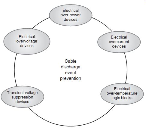
FIG. 18 Telecommunication CDE test system
13.1 Cable Discharge Event Failure--Connector Failure
CDE can fail in cable connectors. Cable connectors are designed to survive certain ESD levels. For example, a registered jack 45 (RJ-45) connector is rated to a given ESD robustness.
Given that the current level or voltage level is exceeded, failure can occur in the RJ45 termination.
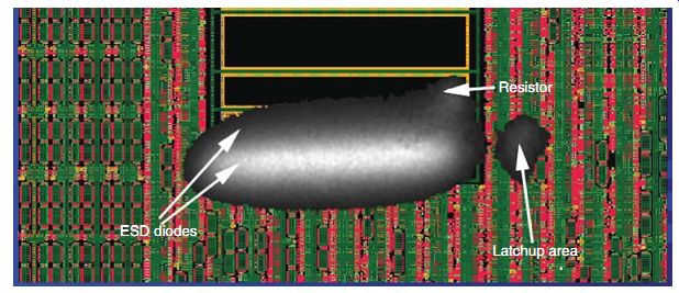
FIG. 19 Cable discharge-induced latchup
13.2 Cable Discharge Event Failure--Printed Circuit Board
CDE can fail in the PCB. Failure can occur between the traces of a PCB leading to impact to the dielectric material or metallization patterns. The failure between adjacent traces will be a function of the physical spacing between the traces.
13.3 Cable Discharge Event Failure--Semiconductor On-Chip
CDE can lead to failure in semiconductor chips that are connected to the cable inputs. Semi conductor failure can occur in the ESD protection circuits or the input/output circuits. In the case of receiver elements, the receiver failure can include dielectric breakdown, and MOSFET second breakdown. Passive and active elements can fail from the CDE event.
13.4 Cable Discharge Event (CDE)-Induced Latchup
CDE can lead to failure in semiconductor chips due to CMOS latchup [26]. Given that the CDE exceeds the latchup tolerance of the semiconductor chip, latchup can occur. Given that the tetrode condition for latchup is satisfied, latchup can occur in I/O or internal circuitry. Latchup will lead to permanent damage to the semiconductor chip. This is discussed in Section 11 (FIG. 19).
14. Cable Discharge Event (CDE) Protection
CDE system level solutions exist to avoid system level failures (FIG. 20). Solutions can be provided with system level PCB design, touch pads, crowbars, and handling procedures to electrical connectors.
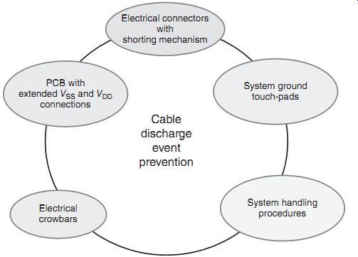
FIG. 20 Cable discharge event (CDE) system level solutions
14.1 RJ-45 Connectors
CDE can lead to arcing in the RJ-45 connectors. RJ-45 connectors are used for UTP. RJ-45 connectors should be used that can withstand large transient voltages. The IEEE 802.3 standard requires for an isolation voltage of 2250V direct current (DC) and a 1500V alternating current (AC).
14.2 Printed Circuit Board Design Considerations
CDE can lead to PCB failures of dielectric breakdown and spark discharge. To avoid PCB failures, the traces from incoming signal of the UTP should be separated from the ground traces. The spacing of at least 250 mils is recommended to withstand 2000V transient events.
14.3 ESD Circuitry
CDE can lead to high voltages in semiconductor components. The CDE that enters the semi conductor chip can lead to input and output circuit failure. ESD protection circuitry can be placed off-chip and on-chip to eliminate failure of the components [15-32]. CDE protection devices can include Schottky, Zener, or silicon diodes, as well as silicon controlled rectifiers networks. Due to the oscillatory nature of the CDE, it is best to provide an ESD circuit solution that is bidirectional (e.g., dual-diode or bidirectional SCR circuitry).
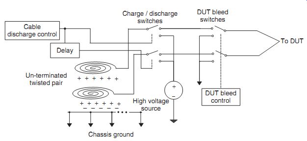
FIG. 21 Cable discharge event (CDE) validation test system
14.4 Cable Discharge Event (CDE) ESD Protection Validation
To verify that the ESD protection is adequate, a validation process can be initiated for the CDE.
A test procedure can be performed using a test system that allows for the charging of the cable, and discharging to the DUT through relays and switching system. In the test system, a delay can be introduced to evaluate the discharge with differential inputs.
FIG. 21 shows a CDE validation test system. A test system is needed to evaluate both common mode and differential mode events. The test system comprises of a cable, a high-voltage generator source, and switches. Switches are needed for the charging process. In addition, a cable discharge control switch is placed in the system, as well as a delay network.
At the DUT, switches are needed to discharge the device using a bleed circuit.
The high-voltage generator source charges the cable relative to the chassis ground. For a CAT5 cable, the relay switches are RJ-45 connectors. The switches to the DUT are then closed, applying the CDE. After testing, the residual charge is removed from the device through a bleed network.
The delay network simulates the insertion process of the cable allowing for evaluation of differential pair voltage differences. A contact delay is introduced that can be varied to evaluate different insertion events. The delay process introduces a differential voltage between the two connections of the differential pair, leading to a differential voltage at the inputs of the DUT.
15. Alternative Test Methods
Alternative test methods can exist for specific applications associated with automobile industry, military, and space applications. Alternative test methods can also exist for different cable lengths outside of the scope of this section. This discussion will provide a base of understanding for measurement, testing, and the issues of CDEs.
16. Summary and Closing Comments
This section addressed a new semiconductor chip level test to address a CDE. This test, the CDE, introduces a fast transient followed by a slower square-pulse waveform. With the growing increase of ports and smaller systems, CDEs are of interest for both chip developers and system designers.
Section 11 discusses CMOS latchup. CMOS latchup physics and theory are briefly discussed, followed by test methods and issues. CMOS DC and transient latchup will be high lighted as well as "internal latchup" versus "external latchup."
Problems:
1. Why are cables an issue in electronic systems?
2. How does one define a cable? What are the electrical characteristics that make a component a cable?
3. Draw a cable as a distributed LC electrical model highlighting the incremental nature of the cable.
4. Draw a cable as a distributed LRC electrical model highlighting the incremental nature of the cable.
5. A package can be represented as a Pi-network of a capacitor-inductor-capacitor. What is the difference between a package and a cable?
6. Explain the charging and discharging process of a cable into a system.
7. A cable has a BNC connector on the end of the cable, and the system also has sockets to socket the BNC connector. Explain the discharge process.
8. A system engineer drags a cable on the floor and sockets the cable into a system. Explain the charging process of the cable, the system engineer, and the charge transfer to the system.
9. In a corporation with large servers, procedures are established to avoid discharging cables into a large server. What procedure can be developed to avoid discharging the cable into the system?
In a corporation with large servers, procedures are established to avoid a system invention on the chassis of the large server. What was the solution?
11. Cable discharge current magnitude can exceed the JEDEC latchup test standard current magnitude. Explain how CMOS latchup can occur from a cable discharge event.
References
[not listed]