AMAZON multi-meters discounts AMAZON oscilloscope discounts
1. History
Complementary metal-oxide semiconductor (CMOS) latchup is a fundamental issue inherent in CMOS technology. Latchup was discovered in CMOS technology in the early 1970s at the beginning of CMOS technology. In many corporations, latchup was first discovered with the first CMOS technology manufactured. CMOS was developed for low power, and many of the first efforts to focus on low power were space applications. A significant amount of understanding was first established at national laboratories and universities. One of the first publications was in 1973 by B.L. Gregory, and B.D. Shafer of Sandia Laboratories, titled "Latchup in CMOS integrated circuits," in the IEEE Transaction on Nuclear Science [9]. The first textbook was introduced in 1985, by R. Troutman, titled "Latchup in CMOS Technology: The Problem and the Cure". The second book on latchup was published in 2007, capturing the advancements between 1984 and 2007 [2].
FIG. 1 illustrates the evolution of latchup testing. In the 1960s, Fairchild Semiconductor invented CMOS technology. In the early 1970s, research continued on CMOS latchup to mainstream integration of CMOS. In the 1970s, laboratory test systems were constructed in laboratories to do latchup testing. There was no standard test structure to test or measure latchup phenomena. Latchup test structure standardization was established in the mid-1980s (within the IEEE) as a means of benchmarking technology for latchup robustness. In the 1980s, commercial test equipment was established for latchup testing. One of the first commercial latchup test systems was developed by Stag Microsystems Inc. called the Verifier. The Stag Microsystem's Verifier was developed for 256-pin testing.
FIG. 2 illustrates a semiconductor chip cross section. Latchup occurs in semiconductors with the formation of a parasitic pnpn structure. The parasitic structure is present in a single-well or dual-well CMOS technology. From the p-channel MOSFET structure, there is a parasitic pnp bipolar junction transistor (BJT) formed from the p+ diffusion MOSFET implant, the n-well tub region, and the p-substrate. From the n-channel MOSFET structure, there is a parasitic npn BJT formed from the n+ diffusion MOSFET implant, the p-substrate, and the n-well region.
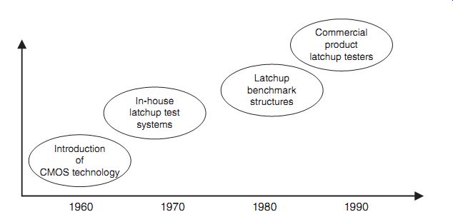
FIG. 1 Latchup testing evolution
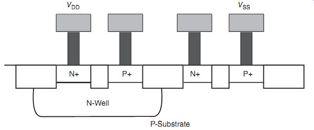
FIG. 2 Latchup cross section
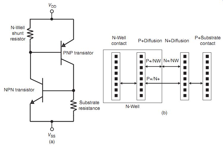
FIG. 3 (a) Latchup two transistor representation. (b) Latchup four-stripe
PNPN test structure
In this structure, the pnp and npn transistors form a four region device, forming a pnpn. Latchup occurs due to the regenerative feedback from the cross-coupled pnp and npn transistor.
FIG. 3 illustrates the electrical schematic representation of a CMOS latchup structure. The schematic shows two transistor representations that are cross-coupled. Latchup occurs in semiconductors with the formation of a parasitic pnpn structure formed by the cross-coupled parasitic pnp BJT and the parasitic npn BJT. In the electrical circuit schematic, there is a first resistor element representing the n-well resistance, RNW, and a second resistor element representing the p-well resistance, RPW. The n-well resistor element is the resistance between the n-well contact and the PFET device. The p-well resistor element is the resistance between the p-well contact and the NFET device.
In order to characterize the latchup sensitivity of a technology, a simplified four-stripe structure can be formed representing the physical dimensions representing the four physical elements (e.g., two transistors and two resistors). FIG. 3(b) represents a simple test structure used to characterize CMOS latchup. The p+ diffusion stripe in the n-well represents the CMOS p-channel MOSFET diffusion. The n+ diffusion stripe in the p-well represents the CMOS n-channel MOSFET diffusion. The n+ diffusion within the n-well region represents the n-well contact. The p+ diffusion within the p-well region represents the p-well (e.g., p-substrate) contact.
The electrical state of the circuit is a function of the electrical characteristics of the four physical elements (e.g., the two transistors and the two resistors). Latchup occurs when the state of the circuit switches from a low current/high voltage state to a high current/low voltage state. When the pnpn structure is in a high current state, Joule self-heating occurs leading to thermal failure of the circuit.
FIG. 4 represents the current-voltage (I-V) characteristic of a CMOS latchup pnpn structure. The I-V characteristic has a first low current "off-state." This state continues with an increasing voltage, until the circuit is in an avalanche multiplication state. The latchup structure "switches" to a conducting region in the "negative resistance" region. The negative resistance state is an unstable state; hence, the circuit recovers into stable low voltage/high cur rent state. When the circuit is in this state, the BJT's current gain increases from self-heating. The circuit can continue in this mode, leading to thermal breakdown.
2. Purpose
The purpose of the latchup test is for establishment of a test methodology to evaluate the repeatability and reproducibility of components or microelectronic circuitry to a defined pulse event in order to classify or compare latchup sensitivity levels of components.
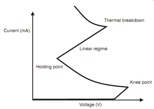
FIG. 4 Latchup current-voltage (I-V) characteristic.
3. Scope
The scope of latchup test is for the testing, evaluation, and classification of components and micro- to nano-electronic circuitry. The test is to quantify the sensitivity or susceptibility of these components to damage or degradation to the defined latchup test.
4. Pulse Waveform
For latchup testing, specific waveforms and bias conditions are defined for testing. These bias conditions and states are specified in the JEDEC JESD78 standard specification.
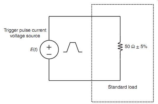
FIG. 5 Latchup waveform for DC latchup
FIG. 5 represents the waveform specification for the CMOS latchup testing.
For transient latchup testing, a pulse is applied to the test structure or system. FIG. 6 represents the waveform specification for the CMOS latchup testing.
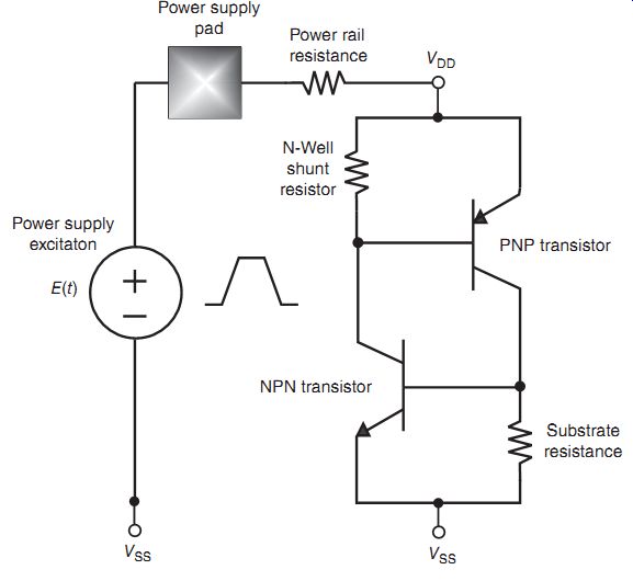
FIG. 6 Transient latchup waveform
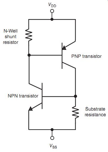
FIG. 7 Latchup equivalent circuit model
5. Equivalent Circuit
An equivalent circuit representation for CMOS latchup can be defined from the test system. FIG. 7 represents the equivalent circuit for the latchup test system and latchup structure.
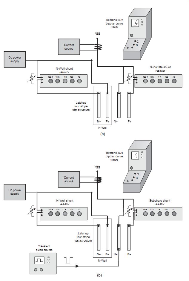
FIG. 8 Example wafer level latchup test system.
6. Test Equipment
For CMOS latchup testing, there is testing that is completed on test structures for semiconductor process and device development, and second, latchup testing on products for reliability, quality, and product assurance qualification and release.
Latchup testing on test structures are typically performed on a wafer level [2]. Wafer level test systems are used to develop semiconductor process technology, design rules, and physical dimensions. The wafer level systems are used to quantify the dimensional rules that influence the parasitic pnp transistor, the npn transistor, the n-well resistance, and the p-well resistance.
Wafer level testing can be performed on different types of test structures, from simple four-stripe structure to more complex structures. FIG. 8 represents an example of a wafer level test system used for testing a four-stripe structure.
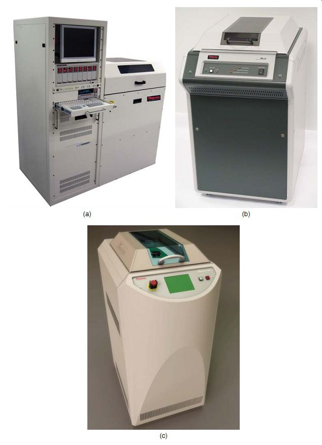
FIG. 9
Thermo Scientific MK4 commercial latchup test system ( Thermo Fisher Scientific)
FIG. 9 is an example of a commercial test system, the Thermo Scientific MK4 for component level latchup testing [39]. This latchup test system satisfies the JEDEC JESD 78D and AEC Q100-004 testing standards. The tester includes preconditioning, state read-back, and full control. It has six independent vector voltage levels allowing for support testing of complex I/O circuitry and multicore products. The test system provides the latchup stimulus and the device biasing.
7. Test Sequence and Procedure
FIG. 10(a) illustrates a latchup test procedure and test low as shown in the JEDEC JESD78 specification [38]. Prior to the latchup test, the device needs to be at stable state with a reproducible nominal current. The supply current must be stable enough and low enough to detect the supply current increase from CMOS latchup. A minimum of three devices are to be tested using the "I-test" and the supply overvoltage tests. The devices used are required to pass the ATE testing to the device specification. The devices are subjected to the I-test first. If they pass, the test continues to the power supply overvoltage test.
FIG. 10(b) illustrates a latchup test procedure for a positive I-test. The supply voltage is raised to a maximum supply voltage, and the pin under test is set to the maximum logic high state. A positive current trigger is then applied to determine if latchup occurs. Note that during the test, overshoots may lead to thermal overstress (TOS). FIG. 10(c) is the test procedure for a negative I-test. FIG. 10(b) illustrates a latchup test procedure for a positive I-test. The supply voltage is raised to a maximum supply voltage, and the pin under test is set to the minimum logic low state. A negative current trigger is then applied to determine if latchup occurs. Note that during the test, TOS may be evident in the pin under test response.
The second test, the power supply overvoltage test is initiated if the chip passes the I-test.
The overvoltage test is performed on each supply pin or pin group. The device under test (DUT) is biased during this test. All input pins are set to the maximum logic high level. A voltage trigger source is then applied to the power supply pin. After the trigger source is removed, the supply pin is returned to the state it was before the application of the trigger pulse. The supply current is then measured to determine if latchup occurred in the DUT.
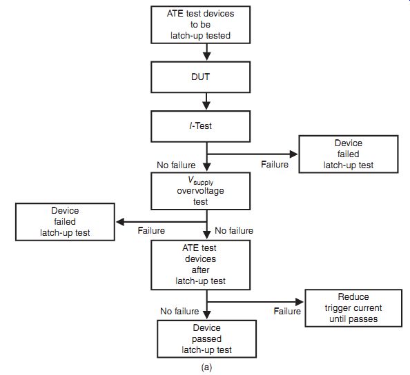
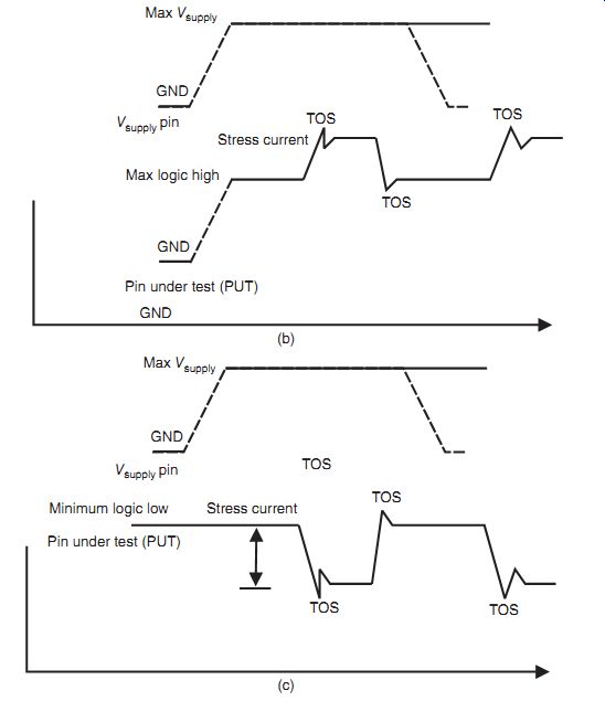
FIG. 10 (a) Latchup test procedure and test low. (b) Latchup test
procedure--positive I-test. (c) Latchup test procedure--negative I-test
8. Failure Mechanisms
Latchup can lead to destructive damage in components to systems. In a semiconductor chip, latchup failure can occur in the following:
• Silicon devices
• Isolation
• Silicides
• Inter-level dielectric (ILD)
• Interconnects
• Bond pads.
FIG. 11(a) is an example of silicon device failure due to a latchup event. In silicon devices, latchup can occur in the parasitic pnp or npn BJT. The silicon damage will occur from junction failure or when the temperature exceeds the melting temperature of silicon.
Other failure mechanisms can occur from silicide penetration of the junctions or metallurgy failure. Interconnect failure can occur in the contacts, vias, or interconnect layers. Interlevel dielectric cracking can lead to failure from the thermal stress of the latchup event.
Latchup failure can lead to semiconductor component package failure [3, 5]. The failure in the package can be the wirebond, lead frame, or package resin materials. The current magnitude from a latchup event can lead to melting of wirebonds and package material. The Joule heating from the latchup event can lead to the physical package ablation, material separation, and physical package melting. A latchup event can lead to melting of the package, preventing separation from the printed circuit board. FIG. 11(b) is an example of package failure from a latchup event.
9. Latchup Current Paths
In latchup, the current path for the latchup event is a function of whether the event occurs intracircuit, in adjacent circuits, or intercircuit. Within a given circuit or adjacent circuits, CMOS latchup currents are contained within the pnpn structure and the resistor elements associated with the pnpn structure. With two adjacent circuits, it is possible that the pnpn structure exists between the two circuits. But there is no current low external to the pnpn and the resistor elements. FIG. 12(a) is an example of a latchup current path that occurs within a single circuit. When the structure undergoes a high current state, the majority of the current exists near and under the isolation where the pnp and the npn are cross-coupled.
In latchup, the current path for the latchup event can be between adjacent circuits. For example, the pnp can be in a first circuit and an adjacent n-well structure can be in an adjacent circuit. In this case, the npn transistor is formed between the first and second circuit. Hence, the pnpn is formed between two circuits. This can occur in the I/O of a semiconductor chip, where I/O are adjacent. In addition, the I/O can be next to a decoupling capacitor that has an n-well structure.
A second case of interest is intercircuit where the injection source of current comes from another region of the chip, outside of the pnpn structure and its corresponding well taps.
In this case, the current stimulus is external to the pnpn and the resistor elements.
FIG. 12(b) is an example of a latchup current path that occurs external to the latchup structure.
10. Latchup Protection Solutions
Protection solutions exist for avoiding CMOS latchup [2]. FIG. 13 highlights different classes of protection from CMOS latchup. CMOS latchup can be addressed by semiconductor process solutions, design layout, circuitry, or system level.
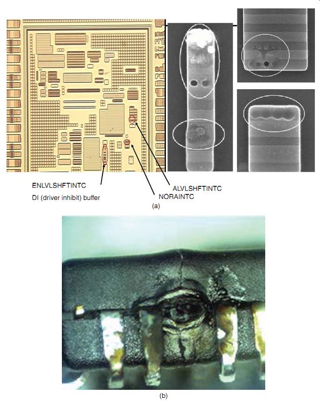
FIG. 11 (a) Latchup failure mechanism--chip level damage. (b) Latchup
failure mechanism--package level damage
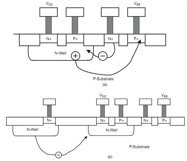
FIG. 12 (a) Internal latchup current paths. (b) External latchup current
paths
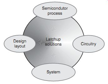
FIG. 13 Classes of latchup protection solutions
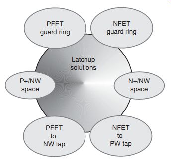
FIG. 14 Latchup design layout solutions--internal
10.1 Latchup Protection Solutions--Semiconductor Process
Semiconductor processes can be developed to provide immunity to latchup events. The process solutions can include the following:
• Retrograde n-well design
• Retrograde p-well design
• Triple well isolation
• Heavily doped buried layer (HDBL)
• Buried Grid (BGR)
• Shallow trench isolation
• Deep trench isolation
• Silicon on insulator buried oxide layer.
10.2 Latchup Protection Solutions--Design Layout
Design layout of circuitry can be used to minimize CMOS latchup sensitivity. Design variables can be separated into intra- and intercircuit latchup design [2].
10.2.1 Latchup Protection Solutions--Internal Design Layout
To decrease a semiconductor design sensitivity to latchup, physical spacing and structure can be used (FIG. 14). The design variables to improve the latchup immunity are as follows:
• Increase the spacing between the p+ diffusion and n-well edge.
• Increase the spacing between the n+ diffusion and adjacent n-well.
• Decrease the n-well tap to PFET spacing.
• Decrease the p-well tap to NFET spacing.
• Place the n-well tap between the PFET and n-well.
• Place the p-well tap between the NFET and adjacent n-well.
• Place guard rings around the PFET.
• Place guard rings around the NFET.
10.2.2 Latchup Protection Solutions--External Design Layout
To decrease semiconductor design sensitivity to external latchup, physical spacing and structure can be used (FIG. 15). The design variables to improve the latchup immunity are as follows:
• Increase the width of the substrate tap.
• Increase the width of the n-well tap.
• Place guard rings around the PFET.
• Place guard rings around the NFET.
• Place guard ring external to complete circuit.
10.3 Latchup Protection Solutions--Circuit Design
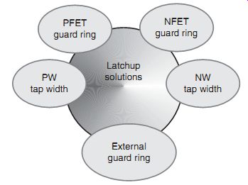
FIG. 15 Latchup design layout solutions--external
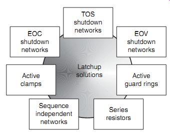
FIG. 16 Latchup circuit design solutions
To decrease semiconductor design sensitivity to latchup, circuit design solutions exist (FIG. 16). Circuit solutions for latchup immunity can include the following:
• TOS shutdown networks
• Electrical overvoltage (EOV) networks
• Electrical overcurrent (EOC) networks
• Sequence-independent power supply system
• Active clamp circuits
• Active guard ring structures
• Resistor elements in series with the power supply.
10.4 Latchup Protection Solutions--System Level Design
To decrease semiconductor design sensitivity to latchup, system level solutions exist (FIG. 17). System level solutions for latchup immunity can include the following:
• Printed circuit board low ground resistance
• Power-up and power-down procedures
• Thermal shutdown networks
• EOV networks
• EOC networks
• Thermal circuit breakers
• Electrical overstress (EOS) protection devices.
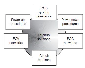
FIG. 17 Latchup system level design solutions
11. Alternate Test Methods
Alternate test methods to study the latchup immunity of systems exist beyond electrical testing. Optical visual techniques are used for latchup integrity to visualize latchup interior to a semiconductor chip. Electrical testing only provides signal pin and terminal characteristics but does not allow for an understanding of the location of latchup within a chip. Different failure analysis techniques include the following:
• CCD photoemission visualization systems
• Picosecond current analysis (PICA) visualization tool
• Liquid crystal techniques
• SQUID imaging technique.
In the following sections, the PICA tool and CCD imaging tool will be used as examples.
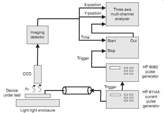
FIG. 18 PICA--TLP test method
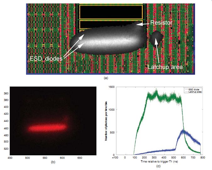
FIG. 19 (a) Photon emissions overlaid on semiconductor chip design.
(b) Photon emissions from ESD diode. (c) Photon emission count versus time
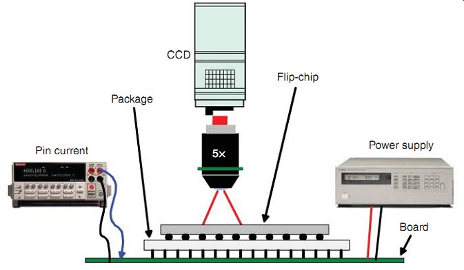
FIG. 20 Photon emission test system
11.1 Photoemission Techniques--PICA-TLP
A photoemission method for characterizing latchup is using a test system that scans the component to determine photoemissions. An advanced test system known as the PICA is shown in FIG. 18. Using a high current source, photon emissions can be detected. A high-quality photo-multiplexer can determine the photon emission in space and time. A trans mission line pulse (TLP) source can apply a pulse train where the photodetector can store and count the photon emissions. In this system, an animation movie can be produced that shows the occurrence of latchup in the test chip. The system can overlay the design layout and the photon emission allowing one to visualize where in the physical design is occurring.
FIG. 19 shows examples of the photon emissions from the test system.
11.2 Photoemission Techniques--CCD Method
A second methodology using photon emission can be a CCD system[35]. The CCD test system is shown in FIG. 20. In this system, the photon emission can also be obtained at different times. FIG. 21(a) and (b) are examples of the photon emission patterns observed from the test system.
12. Single Event Latchup (SEL) Test Methods
A single particle can lead to initiation of latchup in a CMOS technology. This is known as single event latchup (SEL). SEL can occur in space applications. Heavy ions can lead to a latchup event in silicon or gallium arsenide products (FIG. 22).
A testing methodology is to test semiconductor chips or systems in accelerators that produce particles that may lead to CMOS latchup. A test methodology is illustrated in FIG. 23.
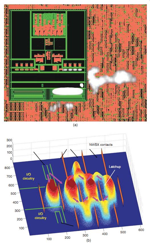
FIG. 21 (a) Photon emission image. (b) Photon emission image (expanded)
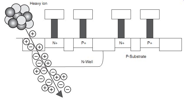
FIG. 22 Single event latchup (SEL)
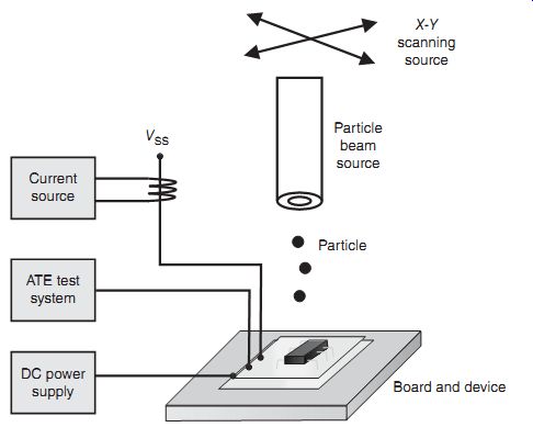
FIG. 23 Testing technique
13. Summary and Closing Comments
This section discussed CMOS latchup. CMOS latchup physics and theory are briefly discussed, followed by test methods and issues. CMOS DC and transient latchup are highlighted as well as "internal latchup" versus "external latchup." The section introduced latchup benchmark test structures and test procedures to quantify the latchup robustness of a technology.
Section 12 looks at the broader issue of EOS. The topic of EOS will be approached providing distinctions of EOS versus ESD phenomena and specific EOS tests that are presently used for systems and for semiconductor chips. EOS failure mechanisms and solutions will be quantified. With the growing increase of system level issues, EOS has been receiving a renewed interest from both semiconductor chip developers and system designers.
Problems
1. What is latchup?
2. Draw a cross section of a CMOS process, and the process of the carrier transport that initiates latchup.
3. Draw a circuit schematic on the cross section of Problem 2 that are fundamental to the latchup process.
4. Draw a circuit schematic between the power supply VDD and substrate VSS highlighting the four fundamental elements involved in the latchup process.
5. Show from the layout how to reduce the likelihood of latchup from layout perspective.
6. Describe the distinction between direct current latchup and transient latchup.
7. Describe the difference between "internal latchup" and "external latchup." Show pictures to describe the distinctions.
8. How from the visual signature of failure analysis can you determine the failure was associated with latchup?
9. How from the electrical signature can one determine the failure was associated with latchup?
10. What is the distinction between long-pulse TLP and CMOS transient latchup testing?
References
[not listed]