AMAZON multi-meters discounts AMAZON oscilloscope discounts
1. History
The machine model (MM) test is another electrostatic discharge (ESD) standard that was used in the industry for many years to qualify components. The MM standard was supported by the ESD Association standards work group; the last version as a standard was ANSI/ESD ESD-STM5.2 - 1999. MM test simulation is integrated into commercial ESD test systems that support both the human body model (HBM) and MM test simulation.
The MM event was intended to represent the interaction of the electrical discharge from a conductive source, which is charged, with a component or object. The model assumes that the "machine" is charged as the initial condition. The charged source then touches a component or object. In this model, an arc discharge is assumed to occur between the source and the component or object, allowing for current transfer between the charged object and the component or object.
The MM event was incorporated into a majority of commercial test systems since it is compatible with the HBM event. In some systems, the pulse source was interchanged to test either HBM or MM events.
2. Scope
The scope of MM ESD test is for testing, evaluation, and classification of components and micro- to nano-electronic circuitry. The test is to quantify the sensitivity or susceptibility of these components to damage or degradation to the defined MM test.
3. Purpose
The purpose of the MM ESD test is for establishment of a test methodology to evaluate the repeatability and reproducibility of components to a defined pulse event in order to classify or compare ESD sensitivity levels of components.
4. Pulse Waveform
An MM characteristic time is associated with the electrical components used to emulate the discharge process. In the MM standard, the circuit component is a 200 pF capacitor; unlike the HBM standard, there is no resistor component. An arc discharge fundamentally has a resistance on the order of 10-25-Ohm. The characteristic RC decay time associated with the MM test simulation is the arc discharge resistor R and the charged capacitor C. FIG. 1 is an example of the MM equivalent circuit (e.g., without the arc resistance term).
4.1 Comparison of Machine Model (MM) and Human Body Model (HBM) Pulse Waveform
Unlike the HBM waveform, the MM event transitions through positive and negative polarities (Figure 2). The MM pulse oscillation switching from positive to negative currents leads to different current paths through the ESD network and circuitry. The MM event is higher peak current compared to the HBM event, leading to failure level ratio from 5 to 30× lower typically in a semiconductor component. FIG. 3 shows an example of an MM source from a commercial MM test system.
MM events are faster than the HBM event due to the lower series resistance. As a result, MM pulse widths are different than long-pulse electrical overstress (EOS) events. In an MM event, the pulse width is less than the thermal diffusion time, approaching adiabatic conditions.
This is opposite of EOS events whose pulse widths are greater than the thermal diffusion time.
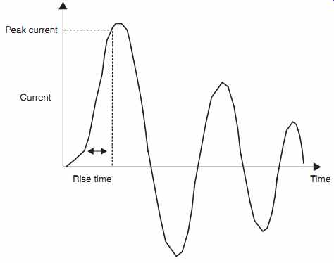
FIG. 1 MM pulse waveform
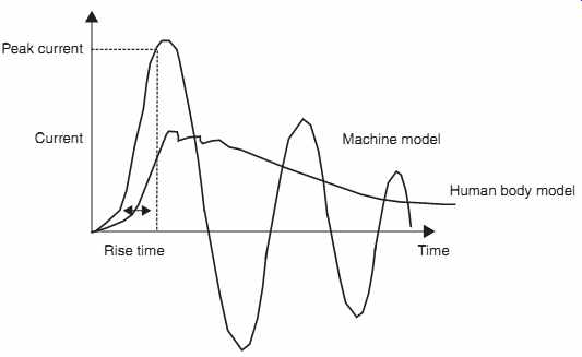
FIG. 2 MM and HBM waveform comparison
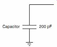
FIG. 3 MM equivalent circuit model
5. Equivalent Circuit
The MM equivalent circuit can be represented as a single capacitor element. FIG. 3 shows the MM equivalent circuit of a 200 pF capacitor.
The MM is influenced by the discharge current, parasitic, and load conditions. FIG. 4 addresses the MM equivalent circuit taking into account the parasitic and load components. In the figure, the discharge path series resistance, the discharge path series inductance, the test board capacitance, and load resistance are shown.
6. Test Equipment
MM commercial test equipment exists for the qualification and release of semiconductor components. FIG. 5(a) shows an example of an MM source for an early commercial MM test system. In these sources, the capacitor element is a module that can be placed in the commercial tester.
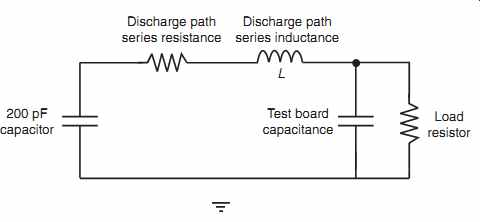
FIG. 4 MM equivalent circuit model with parasitics
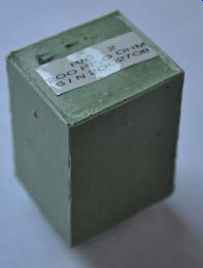
FIG. 5 MM source
MM commercial test equipment will be required to release an MM pulse to the device under test (DUT). The commercial test equipment must have a high-voltage source used to charge the MM source circuit. A switch is contained within the test system that is closed when the high-voltage source charges the equivalent circuit. A second switch must be open during the charging of the MM source circuit. The second switch is closed when the MM circuit current is discharged into the load or DUT.
FIG. 6(a) shows an example of a present-day MM ESD commercial test system. This test system is the Hanwa HCE-5000 ESD test system. The HCE-5000 is designed for portability, improved use of space, and high cost performance. This test system can perform HBM and MM measurements.
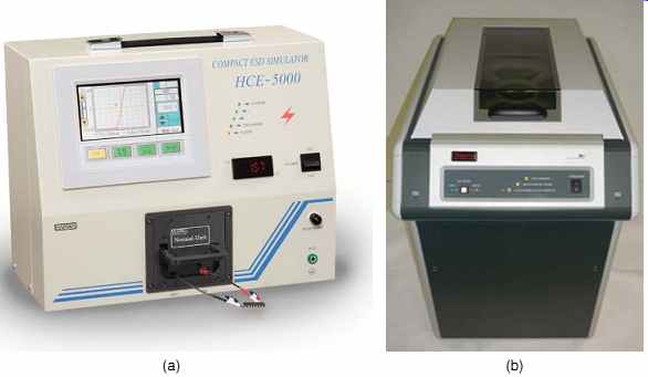
FIG. 6 (a) MM commercial test system. (b) MM commercial test system
- MK1 Thermo-KeyTek (Reproduced with permission of Thermo Fisher Scientific)
The post-testing leakage measurement can be done without an independent computer or a curve tracer. The settings on the test system can be adjusted without an additional computer. This test system satisfies standards for JEDEC, ESDA, AEC, and JEITA standards organizations. Leakage current and curve tracing can be evaluated before and after testing.
The methodology for failure can include percentage change (e.g., 50% shift) or absolute value (e.g., 1 µA). The HCE-5000 charging voltage can be set from 10V to 4 kV, in 5V step increments. The test system can provide both a positive and negative polarity pulse. The leakage voltage accuracy is 1% - +50mV.
FIG. 6(b) is a second commercial test system used for MM testing. This system is the Thermo/KeyTek MK1. The Thermo Scientific MK1 system is an ESD simulator designed for high-yield testing of devices up to 256 pins. The system is a relay-based sys tem that establishes pin combinations by a relay switching matrix. It is 5-10 times faster than robotic-driven ESD testers. The test system addresses the ESDA STM 5.2 specification, as well as JEDEC EIA/JESD22-A115 and AEC Q100-003 specifications. The test system has an MM voltage range from 30V to 1 kV. The system provides a prestress, prefail, and postfail data with full curve tracing capability.
7. Test Sequence and Procedure
In the MM test, there is a test sequence and a procedure. FIG. 7 is a flowchart of the test sequence and procedure for MM testing. In the testing of components to large increments for semiconductor device characterization, a grounded reference is established. An initial reading is performed prior to any applied voltage on the MM source. A first step increment is defined on the capacitor element. All pins are pulsed with an ESD event, individually relative to the grounded reference. Each pin is evaluated based on failure criteria (e.g., voltage shift, leakage).
If a pin "passes," it remains in the test sequence for the next increment. Pins that "fail" are removed from the test sequence, where all other passing pins remain in the test sequence.
The voltage is increased on the capacitor source to the next step level, and testing resumes for the surviving pins. In this case, after the desired steps are taken, the tester is stopped, and the failed pins versus surviving pins are recorded.
In semiconductor corporations that test ESD in-house for characterization or qualification, sometimes a single increment at the test specification standard is completed. In this case, it is "pass-fail" criteria. If all the pins show no degradation after applying the MM pulse to the DUT, then the test is completed.
FIG. 8 is a flowchart of the test sequence and procedure for MM testing where the testing is done in small increments. In the testing of components to small increments for semiconductor device characterization, a first precheck of the pins is performed prior to charging the capacitor source. In small increment testing, a grounded reference is established. A first increment is defined on the capacitor element. All pins are pulsed with an ESD event, individually relative to the grounded reference. Each pin is evaluated based on failure criteria (e.g., volt age shift, leakage). If the pin "passes," it remains in the test sequence. Pins that "fail" are removed from the test sequence, where all other passing pins remain in the test sequence. The voltage is increased on the capacitor source to the next increment level, and testing resumes for the surviving pins. This continues until all the pins have failed the failure criterion. In this methodology, with small increments, the actual failure level is determined for all the pins that are tested, with an accuracy associated with the increment step size.
In semiconductor corporations that in-house ESD test, test in small increments. In older MM test equipment, the smallest increment where accuracy was preserved was 30V increments. In the newer test systems, the increments were reduced to 10V increments. ESD testing would be initiated at 0V as the first evaluation of the leakage characteristic prior to applying a pulse to the DUT. The first voltage increment was then applied to all pins relative to a given reference (e.g., VDD or VSS power pin). A leakage measurement was then taken after application of the pulse event on each pin. All pins that survived the pulse event will continue to be tested to the next test increment. In the case where all the pins are tested to failure, the testing will continue until all the pins have failures. All the results are recorded.
-----------------------
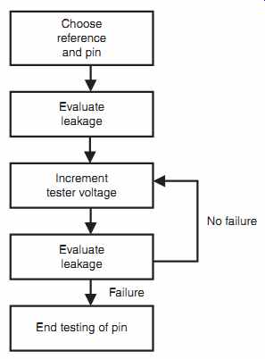
FIG. 7 MM test sequence
Evaluate leakage Evaluate leakage End testing of pin Failure No failure Choose reference and pin Increment tester voltage
-----------------------
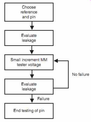
FIG. 8 MM incremental step stress test sequence
Evaluate leakage; Evaluate leakage; End testing of pin; Failure; No failure; Choose reference and pin; Small increment MM tester voltage
---------------------
8. Failure Mechanisms
MM failure mechanisms are typically associated with failures on the peripheral circuitry of a semiconductor chip that are connected to signal pins. MM failures can occur on the power rails due to inadequate bus widths and ESD power clamps between the power rails. MM failures can occur in both passive and active semiconductor devices. The failure signature is typically isolated to a single device or a few elements in a given current path where the current exceeded the capability of the element.
ESD power clamp circuits are designed to be responsive to MM pulse widths; specifically, the RC-triggered MOSFET ESD power clamp is designed for MM events.
MM ESD failures are also distinct from EOS events. MM events will not typically cause failures in the package, printed circuit board (PCB), or single component devices mounted on a PCB (FIG. 9).
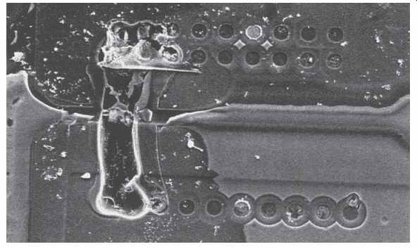
FIG. 9 MM ESD failure mechanisms
9. MM ESD Current Paths
MM event current is oscillatory in nature. The MM waveform is a damped oscillation, which alternates in polarity. As a result, the current path through the circuitry is distinct from HBM, which is a single polarity event. FIG. 10 illustrates an example of a signal pin, with an MM event where the VDD power rail is the grounded reference. During the positive part of the oscillation, the current will flow through the ESD element between the signal pad and the VDD power rail signal pad. As illustrated, an ESD diode element will forward bias to allow current flow to the VDD power pad. For the negative oscillation, the p-n diode between the signal pin and the ground rail VSS will forward bias. ESD current will flow from the VDD power pad, through the VDD power grid, through the ESD power clamp, and back through the diode element connected to the signal pad. After this negative oscillation, it is followed by the second positive oscillation. Hence, during this event, the current is switching current paths as the polarity changes until the MM pulse is completed.
FIG. 11 illustrates an example of a signal pin, with an MM event where the VSS power rail is the grounded reference. During the positive part of the oscillation, the current will flow through the ESD element between the signal pad and the VDD power rail signal pad. As illustrated, the ESD diode element will forward bias to allow current flow to the VDD power rail. The current will flow through the VDD power rail to the ESD power clamp placed between the VDD and VSS power rails. The current will flow through the ESD power clamp to the VSS power rail and VSS bond pad.
For the negative oscillation, the p-n diode between the signal pin and the ground rail VSS will forward bias. After this negative oscillation, it is followed by the second positive oscillation. Hence, during this event, the current is switching current paths as the polarity changes until the MM pulse is completed.
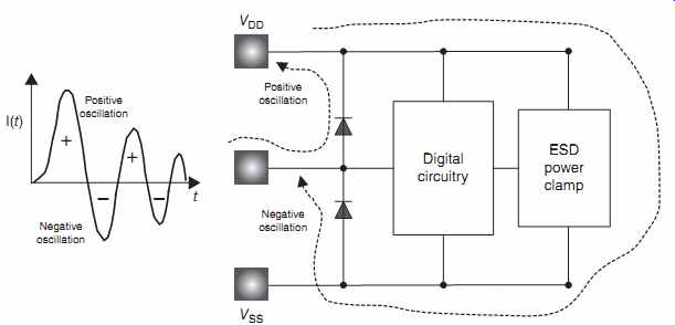
FIG. 10 MM ESD event current paths - signal pin to power (VDD)
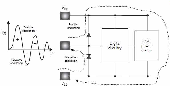
FIG. 11 MM ESD event current paths - signal pin to ground power (VSS)
FIG. 12 illustrates an example of an MM event where the VSS power rail is the grounded reference and the pulse is applied to the VDD power rail bond pad. During the positive part of the oscillation, the current will flow through the ESD power clamp and the power rails. The current will flow through the VDD power rail to the ESD power clamp placed between the VDD and VSS power rails. The current will flow through the ESD power clamp to the VSS power rail and VSS bond pad.
For the negative oscillation, the current will flow in the reverse direction, through the ESD power clamp, as well as through the ESD diode network. After this negative oscillation, it is followed by the second positive oscillation repeating the current flow through the ESD power clamp. Hence, during this MM event, the current is switching current paths as the polarity changes until the MM pulse is completed.
FIG. 13 illustrates an example of an MM event between two ground power rails. Because the ground-to-ground ESD network is bidirectional, current can flow between the two rails for both the positive and negative oscillations.
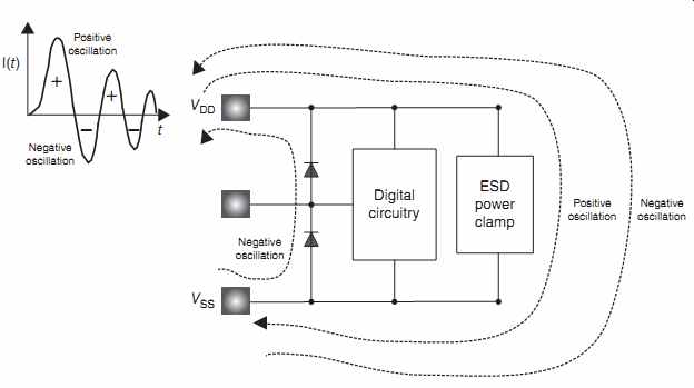
FIG. 12 MM ESD event - power rail (VDD) to ground power rail (VSS)
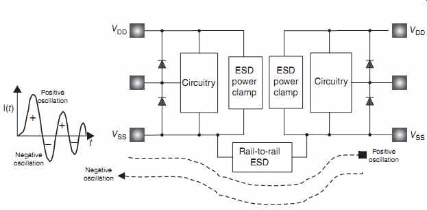
FIG. 13 MM ESD event - power ground (VSS) to ground power rail (VSS)
10. MM ESD Protection Circuit Solutions
To address MM events, ESD protection circuits provide an alternate current path to avoid the sensitive circuit elements. FIG. 14 shows an example of a dual-diode ESD network. For the MM event, the dual-diode circuit addresses both the positive and negative oscillations. For a positive MM test, the first peak is a positive sinusoidal oscillation, which turns on the first p-n diode connected to the power supply VDD. For the first negative oscillation, the second p-n diode is turned on between the n-cathode and the p-substrate. The dual-diode ESD network is a natural solution for this type of event.
FIG. 14 MM ESD protection circuits - dual diode
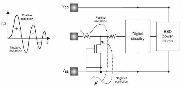
FIG. 15 MM ESD protection circuits - grounded gate NMOS (GGNMOS)
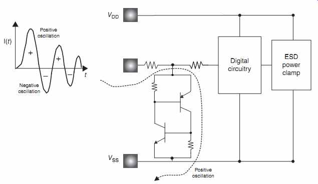
FIG. 16 MM ESD protection circuits - bidirectional silicon controlled
rectifier (SCR)
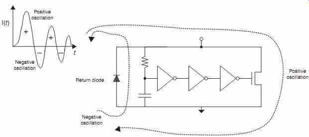
FIG. 17 MM ESD protection circuits - VDD to VSS power rail RC-triggered
power clamp network and return diode
FIG. 15 shows an example of a grounded gate n-channel MOSFET (GGNMOS) ESD network. For the MM event, the GGNMOS circuit addresses both the positive and negative oscillations through MOSFET snapback and forward bias of the MOSFET drain. For a positive MM test, the first peak is a positive sinusoidal oscillation, which turns on the MOSFET through MOSFET snapback. For the first negative oscillation, the second p-n diode is turned on between the n-doped MOSFET drain and the p-substrate.
FIG. 16 shows an example of a bidirectional silicon controlled rectifier (SCR) ESD network [19]. For the MM event, the bidirectional SCR circuit addresses both the positive and negative oscillations through pnpn turn-on. For a positive MM test, the first peak is a positive sinusoidal oscillation, which turns on the SCR from the signal pin to the ground rail. For the first negative oscillation, a second SCR is turned on between the ground rail and signal pad.
FIG. 17 shows an example of an ESD network utilized between the VDD and VSS power rails. This commonly used circuit is known as an RC-triggered MOSFET ESD power clamp.
The RC network is tuned to respond to an MM pulse to allow turn-on of the MOSFET between VDD and VSS. For a positive MM test, the first peak is a positive sinusoidal oscillation, which turns on the RC-trigger network from the VDD to VSS rail. For a negative oscillation, the current flows through the "return diode" placed between the two power rails.
In many corporations, the ESD power clamp consists of two circuits for the different polarity pulse events. Hence, a "return diode" is used to clearly define an ESD solution for the current flowing from the VSS power rail to the VDD power rail. In the case of a MOSFET-based RC-triggered power clamp, there is a large n-diffusion drain on the MOSFET that forms a p-n diode between VDD and VSS.
FIG. 18 MM ESD protection circuits - VSS-to-VSS rail-to-rail network
FIG. 18 shows an example of an ESD network utilized between two VSS power rails. This circuit is designed to be bidirectional. The bidirectional nature of this circuit makes it a natural solution for the MM event. For a positive MM test, the first peak is a positive sinusoidal oscillation, which turns on the p-n diode string from the VSS to VSS rail. For a negative oscillation, the current flows through the "return diode string" placed between the two power rails.
11. Alternate Test Methods
Alternate test methods exist in the industry for testing of components and systems. In this section, the small charge model (SCM) ESD test is discussed.
11.1 Small Charge Model (SCM)
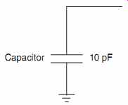
FIG. 19 Small charge model (SCM) equivalent circuit (Hanwa Corporation)
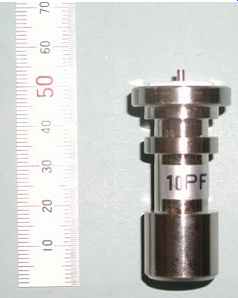
FIG. 20 Small charge model (SCM) source (Hanwa Corporation)
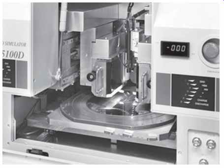
FIG. 21 Small charge model (SCM) commercial tester
An ESD test model is known as the small charge model (SCM) is used in many corporations.
For some customers that use the SCM, it is also known as the Cassette Model. This is also used in the game industry, and many refer to it as the Nintendo model. FIG. 19 shows an SCM source equivalent circuit. The small charge source is a 10 pF capacitor element that placed inside a commercial tester.
FIG. 20 shows an SCM source. The small charge source is a 10 pF capacitor element that placed inside a commercial tester. For test systems and semiconductor suppliers that do not have an SCM source, a "charge equivalency" is established for the MM test; a target is defined for the MM test that will establish equivalency.
FIG. 21 shows an SCM commercial test system. Test system parasitic must be low due to the smaller capacitor element used for testing. The wafer level ESD tester the Hanwa HED-W51000D can perform MM and SCM tests on wafer. This fully automatic MM and SCM test system can test wafers of 300mm. This test system is in conformance with the JEITA, ESDA, and JEDEC test standards.
Since many suppliers do not have an SCM commercial tester, it is possible to use an MM ESD test system and evaluate the correlation between the SCM and MM ESD tests. This is possible, since there is a correlation between the SCM test and the MM test. For example, the MM can be used to verify the desired level needed for passing the SCM test requirement. As a result, corporations that desire passing the SCM test will request a certain magnitude that is achieved in the MM test for qualification.
12. Machine Model to Human Body Model Ratio
In the testing of components, there exists a relationship between the MM results and the HBM test results. A plot can be defined, which plots semiconductor chip results, with the HBM and MM results on the x-axis and y-axis. Experimental results show that the ratio of HBM-to-MM ESD results can be a value of 10×. Although this is the most often quoted HBM-to-MM ratio, this value can range between 5× and 20x.
FIG. 22 shows an example of HBM versus MM plot for semiconductor components.
The plot shows the HBM-to-MM ratio superimposed on the plot for the ratio of 5:1, 10:1, and 20:1. As can be observed from this sample of data, the HBM-to-MM ratio can vary from 5:1 to 20:1. For this semiconductor technology, and product type, the data falls mostly between 10:1 and 20:1. As a result, the MM results were lower than expected.
Another representation of the results is to plot the HBM-to-MM ratio versus HBM.
FIG. 23 shows an example of HBM-to-MM ratio versus HBM plot. From the results, it can be observed that the HBM-to-MM ratio can vary between superimposed on the plot from to over 20:1. In the case that a product must pass the ESD specification for HBM, and MM testing, an awareness of the ratio for a technology, design or corporation.
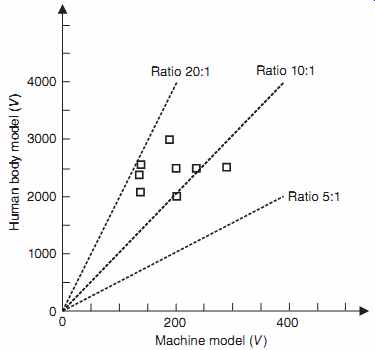
FIG. 22 HBM to MM ratio
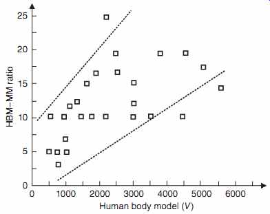
FIG. 23 HBM to MM ratio versus HBM voltage
13. Machine Model Status as an ESD Standard
Today, there is an effort to downrate the MM test as a standard. Historically, this test was valuable to determine the response to an oscillatory non-damped waveform. Using this test in conjunction with the HBM, is important to determine the robustness of devices, components, and systems. As discussed in the preceding section, the ratio of HBM to MM ESD results can vary from 5:1 to 20:1. As a result, if the product has a 20:1 ratio, then the HBM results must be significantly high in order to achieve a good objective for MM results.
In relevance to EOS, the MM test has a higher peak current than that of the HBM standard test. In addition, for EOS analysis, the MM test is similar to the IEC 61000-4-5 surge test in its two polarities.
14. Summary
In this section, one of the most important tests in the history of ESD testing, the MM standard, is discussed. This section focused on model (HBM) purpose, scope, and waveform to test procedures and in addition indicated many of the present and future anticipated changes that will occur on this test. The changes include sample testing, rotation testing, to two-pin test methods. An important issue of the correlation of the HBM and MM test is discussed, as well as the ramification of this correlation issue.
In Section 4, the charged device model (CDM) test is discussed. The CDM is also an important test standard in today's semiconductor chip development. Section 4 highlights the test procedures as well as the current paths and failure mechanisms.
Exercises
1. Assume the 200 pF capacitor of the MM source is charged to a given voltage, and assume a chip of capacitance Cchip is uncharged. The switch is closed. Calculate the net voltage on the chip, assuming the resistance of the switch is zero.
2. Assume the 10 pF capacitor of the SCM source is charged to a given voltage, and assume a chip of capacitance Cchip is uncharged. The switch is closed. Calculate the net voltage on the chip, assuming the resistance of the switch is zero.
3. Assume a semiconductor chip has a dual-diode ESD network on its signal pad, and an RC-triggered MOSFET power clamp between VDD and VSS. Assume that there is a diode between VDD and VSS in parallel with the RC-triggered circuit. Show the current paths through the first four oscillations of the MM pulse.
4. Assume a semiconductor chip has a dual-diode ESD network on its signal pad, and an RC-triggered MOSFET power clamp between VDD and VSS. Assume that there is no diode between VDD and VSS in parallel with the RC-triggered circuit. Show the current paths through the first four oscillations of the MM pulse. What is different from Problem 3?
5. Given the ratio of HBM to MM results of a product is 20:1, what HBM level should a product achieve, given that the MM specification is 200V?
6. Given the ratio of HBM to MM results of a product is 10:1, what HBM level should a product achieve, given that the MM specification is 200V?
7. A technology team's goal for qualification is 2000V HBM and 200V MM ESD specification. In order to pass both specifications, what is the maximum ratio of HBM to MM that is acceptable?
8. Two microprocessor chips are pasted together with polymide separated by 10 µm of poly imide for a system-on-chip (SOC) application. Assume the chip is 10mm × 20mm in size.
A capacitor is formed between the two chips. What is the amount of capacitance between the two chips? Assume a 20mm× 20mm chip size. What is the capacitance? How does this compare to an MM source capacitance?