AMAZON multi-meters discounts AMAZON oscilloscope discounts
1. History
The charged device model (CDM) is an electrostatic discharge (ESD) test method that is part of the qualification of semiconductor components. The CDM standard is sup ported by ESD Association as ANSI/ESD ESD-STM5.3.1 - 1999. Presently, there are four CDM test standards (ESDA S5.3.1, JEDEC JESD22-C101, AEC-Q100-011 Rev. C, and JEITA ED-4701-300). Each requires different test platform, testing, waveform, and calibration requirements. The CDM event is associated with the charging of the semiconductor component through different charging processes. Charging of the package can be achieved through direct contact charging or field-induced charging processes. The field-induced charging method is called the field-induced charged device model (FICDM).
There is presently an effort to align the CDM standards between the ESD Association and the JEDEC organization by establishing a joint ESDA/JEDEC standard. The ESDA/JEDEC joint standard (JS-002 2014) will replace existing CDM ESD standards JEDS22-C101 and ANSI/ESD S5.3.1. The new joint standard will preserve test systems in the field and improve the waveform measurement process.
In addition, there are multiple types of CDM-like tests. FIG. 1 shows examples of different CDMs. These include the CDM, the socketed device model (SDM), and the charged board model (CBM). The SDM was developed into a standard but was eliminated as a standard after years of research and development [60, 61]. It was found that there was inductive coupling of signals in the test system, leading to faulty response. The CBM is presently under development toward a standard.
2. Scope
The scope of CDM ESD test is for the testing, evaluation, and classification of components and micro- to nano-electronic circuitry. The test is to quantify the sensitivity or susceptibility of these components to damage or degradation to the defined CDM test.
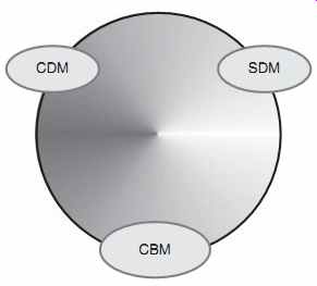
FIG. 1 Charged device models - CDM, SDM, and CBM
3. Purpose
The purpose of the CDM ESD test is for establishment of a test methodology to evaluate the repeatability and reproducibility of components to a defined pulse event in order to classify or compare ESD sensitivity levels of components.
4. Pulse Waveform
The CDM pulse waveform and its comparison to other ESD models are shown in the following sections. Presently, there are four CDM test standards (ESDA S5.3.1, JEDEC JESD22-C101, AEC-Q100-011 Rev. C, and JEITA ED-4701-300) with different waveform requirements.
4.1 Charged Device Model Pulse Waveform
The CDM pulse is regarded as the fastest event of all the ESD events. FIG. 2 shows a CDM pulse waveform. Note that the CDM pulse waveform is influenced by the test platform and measurement metrology. The test platform is influenced by the field plate, field plate dielectric thickness and material type, and the probe assembly (e.g., test head and ground plane). The metrology is influenced by the oscilloscope and verification module specifications.
First, the event is oscillatory. The CDM current pulse rise time is on the order of 250 ps, and with peak currents in the range of 10A. The energy spectrum of the CDM pulse event extends to 5GHz frequency. The CDM pulse waveform has a fast current pulse. The timescale of the CDM event is significantly lower than the thermal diffusion time; hence, CDM events are in the "adiabatic regime" of a Wunsch-Bell power-to-failure curve. CDM events are thus at the opposite direction of long-pulse electrical overstress (EOS) events.
In the calibration and verification procedure, the JEDEC standard requires a 1GHz oscilloscope, whereas the ESDA standard requires 3GHz. Both standards today are bandwidth-limited signal since the CDM waveform is faster than 1GHz. These oscilloscopes were chosen based on availability at the time. It is well known that the energy spectrum of the CDM pulse waveform can extend into the 5GHz frequency.
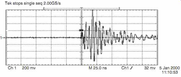
FIG. 2 Charged device model pulse waveform
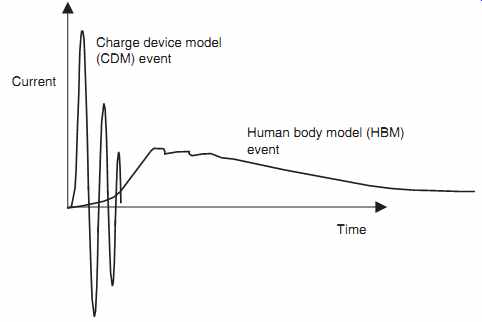
FIG. 3 Charged device model (CDM) and HBM waveform comparison
The new joint specification JS-002 will increase the bandwidth requirement to over 6GHz.
In addition, new "test conditions" (TC) of 125, 250, 500, 750, and 1000V will be specified.
Full width half maximum (FWHM) values for minimum and maximum magnitudes will also be specified.
4.2 Comparison of Charged Device Model (CDM) and Human Body Model (HBM) Pulse Waveform
The CDM pulse is significantly different from the human body model (HBM). FIG. 3 shows a comparison of the CDM and HBM events. First, the CDM event is oscillatory, whereas primarily the HBM event is a damped double exponential decay response. Second, the rise time of the CDM event is significantly faster than that of the HBM event. The CDM event rise time is 250 ps, whereas the HBM event rise time is 17-22 ns. Third, the decay time of the CDM event is faster than that of the HBM event. The HBM event is associated with the RC time of the HBM network (e.g., 150 ns).
From a Wunsch-Bell power-to-failure curve perspective, the CDM event is in the adiabatic regime, whereas the HBM event is in the thermal diffusion time regime.
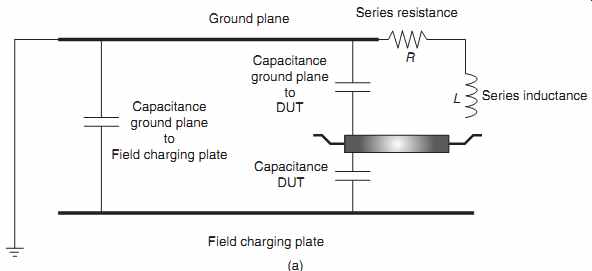
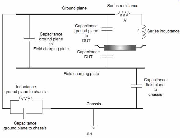
FIG. 4 (a) Charged Device Model equivalent circuit. (b) Charged Device
Model equivalent circuit with parasitics associated with the chassis
5. Equivalent Circuit
The equivalent circuit for the CDM is highlighted in FIG. 4. In the equivalent circuit, the capacitances have the largest influences on the CDM. The test system consists of a field charging plate, the ground plane, and the device under test (DUT). A primary capacitance is the capacitance formed between the DUT and the field charging plate (CDUT). A second primary capacitance is the capacitance of the DUT to the ground plane (Cg). There is also a capacitor formed between the field charging plate and the ground plane (Cgpd). In the discharge process, the discharge is initiated by the pogo pin between the DUT and the ground plane. The equivalent circuit is an inductor and a resistor, shown as a resistor, RS, and inductance LS.
In the equivalent circuit, additional parasitic capacitances can be shown to address the chassis in the test system (FIG. 5). FIG. 4b illustrates three additional circuit elements in the equivalent circuit associated with the chassis. A first capacitor is formed between the field charging plate and the chassis (Cfgc). Between the ground plane and the chassis is an inductor (LC) and capacitance (Cgpc).
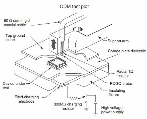
FIG. 5 Charged device model tester
6. Test Equipment
Commercial test equipment has been developed to perform the CDM test. Early CDM test equipment was not commercial but practiced by early developers at AT&T. The first CDM tester was developed at AT&T and was called the "Happy Zapper." Without the standardization of the CDM event, there were issues of the test system's repeatability and reproducibility. The early test system could not verify the release of a pulse event, and hence performed the same pulse five times. Second, the early test systems pulse event was not consistent but showed variation. Third, the CDM response was a function of the insulator thickness and insulator material properties; this led to variation of the CDM event results. These problems were solved with new commercial test systems allowing for repeatable and reproducible results.
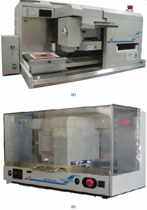
FIG. 6 (a) Charged device model (CDM) commercial test system Hanwa HED-C5000.
(b) Charged device model (CDM) commercial test system Hanwa HED-C5000R (Reproduced
with permission of the Hanwa Corporation)
FIG. 6(a) shows a commercial test system for CDM testing developed in Japan. The figure shows a test system from the Hanwa HED-5000 series. FIG. 6(b) shows a second image of the commercial test system for CDM testing developed in Japan by the Hanwa Corporation. The HED-C5000R CDM test system is in conformance with the JEDEC, ESDA, AEC, and JEITA standard organizations. The system has built-in humidity control and N2 enclosed chamber. The test system provides a wide motion test area (e.g., 80mm× 200mm) allowing for large semiconductor chips to be placed in the test system. The test capability of the HED-C5000R CDM system can test 1024 pin components. The testing voltage can range from 0 to 4000V in step voltage of 5V. The test voltage accuracy is 1% ±10V. The number of pulses can be set for one pulse, or up to 100 times. The interval time between pulses can be changed from 0 to 10 s.
FIG. 7 shows a different commercial test system for CDM testing developed by the Thermo KeyTek Corporation. This test system is the Orion CDM tester. This test sys tem is configurable to different ESD test standards (e.g., JEDEC, ESDA, AEC, JEITA, and CDM2). The system has a high-resolution display to allow for discharge pin alignment during the testing setup. This system has an enclosed test area for moisture control. By controlling the environment for testing, this will insure repeatability when performing an air discharge event (e.g., field-induced CDM (FICDM)). One of the issues with CDM testers is whether the CDM event actually occurred. In this system, an "event detector" is used to confirm the CDM ESD discharge by internal detection and waveform capture. In this system, software exists for evaluation of the waveform performance during device testing. The software package in the test system allows for programming the test voltage, polarity, delay time between pulses, as well as alignment of the chip in the system (e.g., pin coordinates).
7. Test Sequence and Procedure
A test procedure and sequence is required for CDM testing to assure proper testing.
FIG. 8 shows a flowchart of the CDM testing procedure. The CDM event is associated with the charging of the semiconductor component through different charging processes. Charging of the package can be achieved through direct contact charging or field-induced charging processes. The field-induced charging method is called the FICDM. Today, the commercial test system has the sequence of steps for the charging process, as well as for the discharging process (FIG. 8). In the CDM test simulation, discharging is achieved using a pogo pin touching one of the semiconductor component package pins.
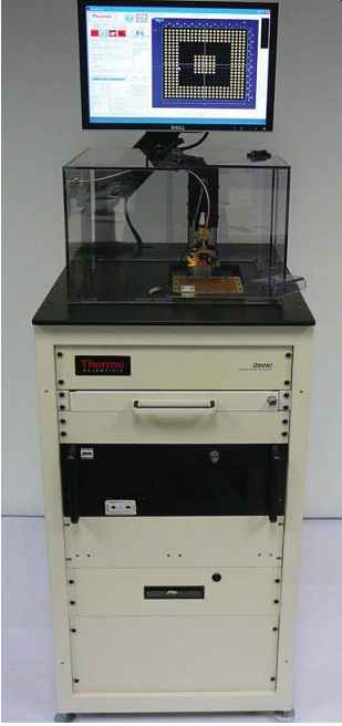
FIG. 7 Charged device model (CDM) commercial test system - Thermo KeyTek
Orion 2 (Reproduced with permission of Thermo Fisher Scientific)
Each requires different test platform, testing, waveform, and calibration requirements.
Presently, there are four CDM test standards (ESDA S5.3.1, JEDEC JESD22-C101, AEC-Q100-011 Rev. C, and JEITA ED-4701-300). The JEDEC standard calibration, a 55 pF large coin (metal only) is used for the test system calibration. For the ESDA standard, it uses a 30 pF target metal disk encased in a 0.88-mm-thick FR4 insulator. For the small coin calibration, JEDEC uses a 6.8 pF coin, whereas ESDA uses a 4.0 pF coin encased in 0.8-mm-thick FR4 insulator. In the calibration and verification procedure, the JEDEC standard requires a 1GHz oscilloscope, whereas the ESDA standard requires 3GHz. Both standards today are bandwidth-limited signal since the CDM waveform is faster than 1GHz.
The new specification will increase the bandwidth requirement to over 6GHz.
Additional differences exist between the JEDEC and JS-002 standards. The JEDEC standard uses a 0.388mm FR-4 dielectric, and in the discharge path, a ferrite and 1 ohm resistor element.
In the new JS-002 standard, there is no ferrite specified. The new joint specification JS-002 will increase the bandwidth requirement to over 6GHz. In addition, new "test conditions" of TC 125, 250, 500, 750, and 1000V will be specified. FWHM values for minimum and maximum magnitudes will also be specified.
-------------------------------
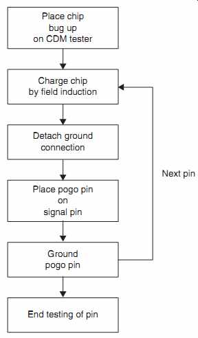
FIG. 8 Charged device model (CDM) test sequence
Place chip bug up on CDM tester Charge chip by field induction Detach ground connection Place pogo pin on signal pin Ground pogo pin End testing of pin Next pin
-------------------------------
For the new test standard, JS-002, the nominal field plate charging resistor is 1000M-ohm.
In the standard, there will be an option for a lower value for large products, to avoid charging resistor delay effects, as well as to improve the current peak measurement for large area/high-capacitance components. The procedure to evaluate the charging resistor effect on large modules is as follows:
• Average of 10 current peak measurements with the charging delay setting to 0ms.
• Average of a second set of current peaks with charging delay of 500ms.
• If the two averages are the same, there is no requirement for a change of charging resistor value.
8. Failure Mechanisms
CDM event damage can occur in the semiconductor chip through the substrate or the power supply. The charge stored on the substrate or the power supply rapidly discharges through the pin that the pogo pin is grounding. CDM event can be small "pin-hole" in a MOSFET gate structure, small transistors in receiver networks, and metal interconnects. FIG. 9 shows an example of a MOSFET gate dielectric failure from a CDM event.
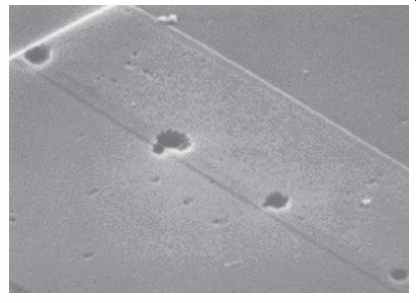
FIG. 9 Charged device model (CDM)-induced failure mechanism - receiver
gate failure
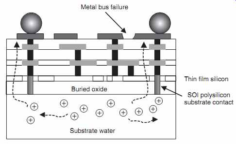
FIG. 10 Charged device model (CDM)-induced failure mechanism - interconnects
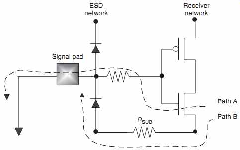
FIG. 11 Charged device model (CDM) ESD event current path - charged
VSS positive polarity and grounded receiver pin
The CDM metal interconnect failure can be significant due to the high current magnitude of the CDM event. FIG. 10 shows an interconnect failure from a CDM event [55].
9. CDM ESD Current Paths
The current path for CDM in components is significantly different from other ESD events. In the case of the CDM, the package and/or chip substrate is charged through a power or ground rail. The component itself is charged slowly to a desired voltage state. As a result, the current flows from the component itself to the grounded pin during ESD testing. This is significantly different from other ESD tests that ground a reference, and then apply an ESD event to a signal or power pin. As a result, the current path that a CDM event follows is from inside the component to the pin that is grounded during test.
FIG. 11 is an example showing the CDM current path from a charged ground rail (e.g., p-substrate) to the grounded receiver pin. For a positive charging of the substrate, the current flows from the substrate to any possible path that will reach the grounded signal pad node. The figure shows two paths: Path A is through the n-channel MOSFET receiver circuit and Path B is through the substrate and the ESD diode.
In the case of the ESD protection circuit is far from the signal pad, the substrate resistance can be significant. For Path B, the total resistance from the grounded location to the grounded signal path is the sum of the substrate resistance and the ESD diode series resistance. In the case that the receiver network is adjacent to the ESD network, or close to the signal to the signal pad, a majority of the current will flow through the ESD network. But, when the ESD network is far from the receiver network, the substrate resistance will be significant. When the impedance of the n-channel MOSFET receiver and the series resistor (e.g., Path A) is low compared to that of Path B, the current will flow through the receiver gate structure, causing rupturing of the MOSFET gate dielectric.
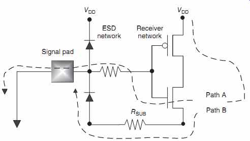
FIG. 12 CDM ESD current paths - charged VDD positive polarity and grounded
receiver pin
FIG. 12 is an example showing the CDM current path from a charged power rail (e.g., VDD) to the grounded receiver pin. For a positive charging of the power rail, the current flows from the power rail to any possible path that will reach the grounded signal pad node. In the figure, two paths are shown. Path A is from the power supply rail to the substrate and then through the n-channel MOSFET receiver circuit. Path B is from the power supply rail, through the substrate, and the ESD diode. When the power supply is charged up to voltages above the n-well-to-substrate breakdown voltage, current will flow to the p-substrate.
As in the last case, if the ESD protection circuit is far from the signal pad, the substrate resistance can be significant. For Path B, the total resistance from the grounded location to the grounded signal path is the sum of the impedance of the n-well-to-substrate diode, the substrate resistance and the ESD diode series resistance. In the case that the receiver network is adjacent to the ESD network, or close to the signal to the signal pad, a majority of the current will flow through the ESD network. But, when the ESD network is far from the receiver network, the substrate resistance will be significant. When the impedance of the n-channel MOSFET receiver and the series resistor (e.g., Path A) is low compared to Path B, the current will flow through the receiver gate structure causing rupturing of the MOSFET gate dielectric. Also note in this case, an additional path is through the reverse-bias p-n diode of the ESD network; this has never been observed as a failure mechanism.
10. CDM ESD Protection Circuit Solutions
For the CDM failures, circuit solutions exist to address low-level failure mechanisms. Additional ESD circuit elements can be added to existing circuitry to solve the CDM to acceptable results.
FIG. 13 is an example of a commonly used CDM ESD network. The ESD net work comprises of a first-stage dual-diode network placed adjacent or in proximity to the signal pad. A second set of diodes (e.g., second-stage network) are placed adjacent to the receiver circuit. A resistor is placed between the first and second stage. FIG. 13 shows the possible paths of the CDM event for the case of a charged substrate. Three paths are shown for the CDM current path from a charged ground rail (e.g., p-substrate) to the grounded receiver pin. For a positive charging of the substrate, the current flows from the substrate to any possible path that will reach the grounded signal pad node. Path A is through the n-channel MOSFET receiver circuit and to the second-stage ESD diode. Path B is through the substrate to the second-stage diode network. Path C is through the substrate to the first-stage ESD network.
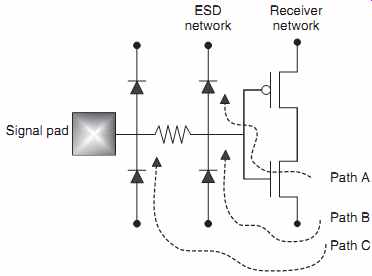
FIG. 13 Charged device model (CDM) ESD protection circuits - dual-diode-resistor-dual-diode
network.
In the case that the first-stage ESD protection circuit is far from the signal pad, the substrate resistance can be significant. For Path C, the total resistance from the grounded location to the grounded signal path is the sum of the substrate resistance and the ESD diode series resistance.
In the case that the receiver network is adjacent to the second-stage ESD network, the current will prefer to follow Path B instead of Path A. When the impedance of the n-channel MOSFET receiver (e.g., Path A) is higher than resistance through Path B, the receiver gate structure can avoid rupturing of the MOSFET gate dielectric. To insure that the current flows through Path B through the second-stage CDM ESD network, the circuit must be close to the receiver, and a low series resistance diode element.
FIG. 14 is an example of a second CDM ESD network. In this network, a first-stage dual-diode network is placed adjacent or in proximity to the signal pad. The second-stage network consists of a series resistor, and a grounded gate n-channel MOSFET placed adjacent to the receiver circuit. In the case of HBM ESD testing, the second stage serves as a resistor divider network, increasing the HBM protection level significantly. For CDMESD protection, the n-channel MOSFET drain serves as a p-n diode element. Placement of the n-channel MOSFET adjacent to the receiver network provides a low impedance path through the MOSFET parasitic p-n diode (Path B). In addition, if the local substrate increases positively, the MOSFET turn-on occurs (Path C). As in the prior discussion, Path B prevents current flow through Path A given that the impedance of the MOSFET gate receiver is higher compared to the series resistance of the substrate and the impedance of the p-n junction of the CDM GGNMOS structure. The current flow through Path D is a function of the proximity of the receiver network to the signal pad and the substrate resistance.
For silicon-on-insulator (SOI) technology, with the separation of the MOSFET from the substrate, the current paths will be different. FIG. 15 shows an SOI circuit and CDM failure mechanism. The CDM current flowed from the p-substrate to the power supply rail VDD.
The CDM current path went from the pass transistor MOSFET gate to grounded signal pad, causing gate-to-diffusion failure. The solution to improve the CDM robustness was placement of a series resistor in series with the pass transistor MOSFET gate, increasing the impedance between the pass transistor and signal pad. In this manner, current flowed through the first-stage ESD elements instead of through the receiver network.
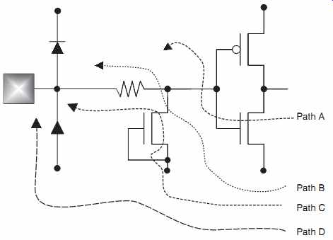
FIG. 14 Charged device model (CDM) ESD protection circuits - dual-diode-resistor-grounded
gate NMOS
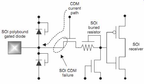
FIG. 15 Charged device model (CDM) failure mechanisms in silicon-on-insulator
(SOI) technology
11. Alternative Test Methods
An alternative test method for CDM evaluation has been proposed. In the following section, the SDM and the CBM are discussed.
11.1 Alternative Test Methods - Socketed Device Model (SDM)
An alternative test method for CDM evaluation was known as the SDM. This test was performed with the semiconductor component socketed into a test board. The semiconductor component was charged to the substrate (e.g., VSS) or power supply (e.g., VDD) by a power supply. The packaged semiconductor chip was then discharged through one of the signal pins.
An SDM standard was established for this test.
The standard practice is ESD Association Standard Practice for Electrostatic Discharge Sensitivity Testing - SDM - Component Level, released in 2013. This standard practice defines a method to verify the correct operational state of the test simulator. It describes a procedure for measuring acceptable SDM discharge waveforms, determines critical waveform parameters and their acceptable values, and provides recommendations for device testing and ESD stressing levels.
In addition, there is a technical report, referred to as ESD Association Technical Report - Socket Device Model (SDM) Tester - An Applications and Technical Report [61]. This technical report provides a detailed description of existing SDM test systems. It defines a waveform confirmation test method, as well as explains why a derating stress voltage method must be used to account for differences in SDM test equipment. The technical report describes the side effects of background tester parasitic RLC transmission line (TL) components and proposes design requirements to be achieved by the next-generation test system. Since this report, the SDM test has been abandoned and is not used nowadays for qualification of semiconductor components.
12. Charged Board Model (CBM)
An alternative test method for CDM evaluation was known as the CBM (as well as the charged board event (CBE)). In the following sections, the charge board model is described (FIG. 16).
------------------
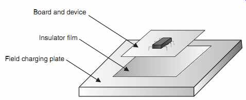
FIG. 16 Charged board model
Board and device; Insulator film; Field charging plate
------------------
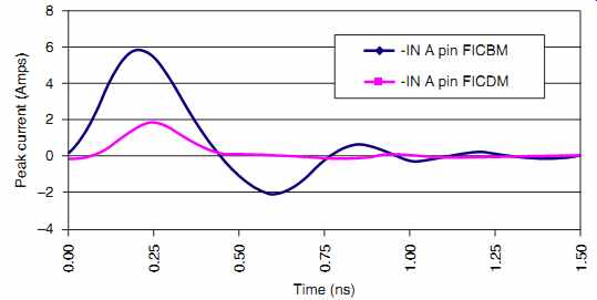
FIG. 17 FICDM and field-induced charged board model (FICBM) waveform
comparison
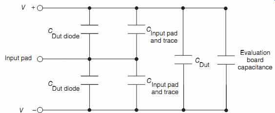
FIG. 18 Equivalent circuit schematic with FICDM and FICBM capacitive
elements
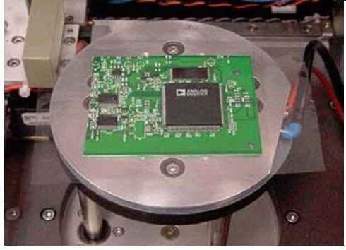
FIG. 19 Field-induced charged board model (FICBM) testing of populated
printed circuit board
12.1 Comparison of Charged Board Model (CBM) and Charged Device Model (CDM) Pulse Waveform
The CBM and the CDM have different waveforms due to the different electrical characteristics involved in the discharge process. First, the field-induced charged board model (FICBM) has a larger capacitance compared to the FICDM due to the printed circuit board (PCB) [48]. Second, the PCB resistance and inductance characteristics are distinct from a component's resistance and inductance characteristics. In the case of the FICBM, the PCB traces have lower resistance than that of the interconnects within the DUT.
FIG. 17 shows a comparison of the waveforms of the FICBM and the FICDM. First, the rise time of the FICBM waveform is faster than that of the FICDM waveform due to the lower inductance and lower resistance of the discharge path of the PCB. Second, the FICBM peak current is significantly higher than the FICDM peak current. The FICBM has a larger effective capacitance due to the addition of the PCB capacitance. The increase in the peak current will lead to lower FICBM ESD protection levels of protection in comparison to the FICDM ESD protection levels.
The increase in the FICBM capacitance is evident from the circuit schematic in FIG. 18.
FIG. 18 shows the capacitance elements from the DUT as well as the additional capacitors from the PCB.
The circuit schematic contains the capacitance of the input diodes to both the power supply and ground rails. In addition, in parallel to these DUT capacitors are the board capacitors to the power supply and ground power planes. In the schematic, the DUT capacitance between the power supply and the ground rail is in parallel with the evaluation board capacitance (FIG. 19).
FIG. 20(a) shows an example of an FICBM failure of an input protection diode. The element in the center of the scanning electron microscope (SEM) image is the anode connected to the negative power supply. The damage in the perimeter is the cathode electrically connected to the cathode. This damage was evident at a -500V FICBM level.
FIG. 20(b) shows an example of an FICBM failure of an input protection diode at a higher test level. The damage in the perimeter is the cathode electrically connected to the cathode. This damage was evident at a -625V FICBM level.
FIG. 20(c) shows interconnect damage from an FICBM event. It is clear that the large damage pattern is a CDM, CBM, or EOS. In this case, it is known that this damage pattern was from an FICBM ESD test.
-------------------
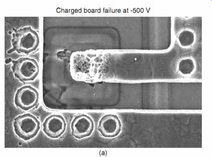
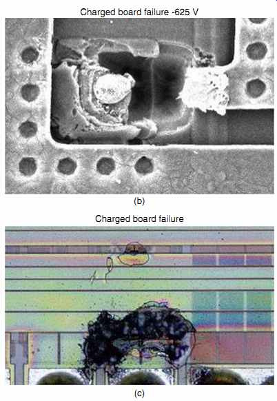
FIG. 20 (a) CBM failure of an ESD diode. (b) CBM failure of an ESD diode.
(c) CBM failure of interconnects
Charged board failure; Charged board failure -625 V; Charged board failure at -500 V
----------------------
12.2 Charged Board Model (CBM) as an ESD Standard
Today, the CBM is not a supported ESD standard. There is a strong possibility that this will be a standard in the near future. This is most critical to small systems, such as cell phones.
13. Summary
In this section, the CDM test was discussed. The CDM is also one of the most important test standards in today's semiconductor chip development. To combat CDM failures, CDM-specific circuitry was integrated into the power grid and input circuitry of semiconductor chips. In addition, new tests are being developed to address chips mounted on the PCB.
In Section 5, again another large step forward in the history of ESD testing is the development of transmission line pulse (TLP) testing standard. An important issue of the correlation of the TLP test to the HBM test is discussed.
Exercises
1. In manufacturing, semiconductor chips are placed on an insulating conveyer belt to avoid scratching of the paint off the metal package of a microprocessor. As the chips are picked up by a manufacturing person, the microprocessor is damaged by CDM. Out of 300 microprocessors, 200 were destroyed due to CDM failures. Explain the complete charging process that leads to this failure. Explain a solution to the ESD failures.
2. In shipping, DRAM chips are placed into a shipping tube. When the DRAMs are removed from the shipping tube, they come in contact with a table top. Explain the charging and discharge process of the chip. Explain how the charge transfers internally in the chip that leads to the interior failure. Explain the circuitry and which pins would fail. Explain the complete charging process that leads to this failure.
3. Magnetic recording heads are placed in a plastic tray that contains carbon to improve the conductivity of the shipping tray. Unfortunately, the extrusion of the carbon was not uniformly distributed in the shipping tray. This problem leads to a high yield loss of magnetic recording heads. Show the charging process within the tray. Explain how to measure the conductivity to determine the problem.
4. Silicon germanium (SiGe) radio frequency (RF) chips are placed in a plastic tray that contains carbon to improve the conductivity of the shipping tray. RF chips were picked up with metal tweezers prior to measuring on a bench station. Fifty percent of the chips were destroyed by the test engineer. Show the charging process and discharging process.
Explain the RF chip failures. Explain how to change the tweezers and manufacturing steps to test these RF components.
5. A semiconductor chip is 20mm × 20mm.Howmuch charge is stored in the chip compared to a 1mm × 1mm chip? What are the CDM ramifications?
6. A semiconductor substrate of a CMOS chip is charged using a 1MO resistor to 1000V to the substrate VSS signal pin. What is the voltage of the VDD power supply?
7. A semiconductor chip is a CMOS chip with a single n-well in a p-substrate. The chip size is 20mm × 20mm. What is the size of the n-well to the substrate diode area?
8. A semiconductor chip is a silicon-on-insulator (SOI) technology. The technologist did not place a substrate contact between the backside of the wafer and the top surface. The substrate region is charged by the testing chuck. Explain the possible CDM failure mechanisms.
9. A semiconductor SRAM chip is a silicon-on-insulator (SOI) technology. The technologist placed a polysilicon substrate contact between the backside of the wafer and the top surface on the edges of the SRAM array. The buried oxide (BOX) region was destroyed by the CDM event. Explain the interrelationship between the charge distribution in the substrate, the buried oxide thickness, the size of the chip, the substrate resistance, and polysilicon substrate contact resistance.
10. CDM circuitry is typically placed local to a MOSFET receiver network. Explain the current paths and all parasitic components of the circuitry and substrate assuming a dual-diode-resistor-dual-diode ESD network. Where are the CDM circuit elements to be placed? What is the interrelationship between the substrate resistance, the placement near the receiver, and size of the CDM circuitry.
11. Given a dual-diode-resistor-dual-diode ESD network, show all current paths from the CDM event to the signal pad when the resistor value is 200-Ohm. How does the current get back to the signal pad? What should be the on-resistance of the CDM diode (e.g., second-stage network)?
12. Given a dual-diode-resistor-grounded gate MOSFET ESD network, show all current paths from the CDM event to the signal pad when the resistor value is 40-Ohm. How does the current get back to the signal pad?
13. Given a dual-diode-resistor-grounded gate MOSFET ESD network, what advantages does this circuit have over the dual-diode-resistor-dual-diode network for CDM, for HBM, and for MM?
14. Show the CDM failure mechanisms of a CMOS receiver network that contains a dual-diode ESD network, followed by a MOSFET half-pass network, and a MOSFET receiver. This circuit is mapped into SOI with no body contacts on the MOSFETs. Show the CDM failure mechanisms now after mapping into SOI. Show the current paths back to the signal pin.